13
Architecture of 8085
![]() Details of 8085 architecture
Details of 8085 architecture
![]() Arithmetic logic unit (ALU)
Arithmetic logic unit (ALU)
![]() Timing and control unit
Timing and control unit
![]() Instruction register (IR)
Instruction register (IR)
![]() W and Z registers
W and Z registers
![]() Temporary (temp) register
Temporary (temp) register
![]() Multiplexer/demultiplexer
Multiplexer/demultiplexer
![]() Address/data buffers
Address/data buffers
![]() Internal address latch
Internal address latch
![]() Incrementer/decrementer
Incrementer/decrementer
![]() Connection of registers to internal bus
Connection of registers to internal bus
![]() Instruction cycle
Instruction cycle
![]() Opcode Fetch (OF) machine cycle
Opcode Fetch (OF) machine cycle
![]() Memory Read (MR) machine cycle
Memory Read (MR) machine cycle
![]() Memory Write (MW) machine cycle
Memory Write (MW) machine cycle
![]() I/O Write (IOW) machine cycle
I/O Write (IOW) machine cycle
![]() I/O Read (IOR) machine cycle
I/O Read (IOR) machine cycle
![]() Comparison of different machine cycles
Comparison of different machine cycles
![]() Memory speed requirement
Memory speed requirement
![]() Earliest data output time considering tACC
Earliest data output time considering tACC
![]() Earliest data output time considering tCE
Earliest data output time considering tCE
![]() Earliest data output time considering tOE
Earliest data output time considering tOE
![]() 27128-20 Compatibility check with 8085AH
27128-20 Compatibility check with 8085AH
![]() Assessing compatibility of 27128-20 with 8085AH-2
Assessing compatibility of 27128-20 with 8085AH-2
![]() Wait state generation
Wait state generation
![]() Questions
Questions
In the previous chapters the effect of execution of majority of the instructions has already been discussed. Just the programmer's view of 8085 was enough to discuss the effect of executing an instruction. For example, the effect of executing LDA C100H instruction is that accumulator gets loaded with the contents of memory location C100H. But the mechanism by which accumulator gets loaded with contents of memory location C100H was not discussed. To know these details, one has to know the architecture of 8085, which is much more complex than the programmer's view of 8085. To provide an -analogy, programmer's view is similar to the driver's view of an automobile. Architectural viewpoint is similar to the mechanic's view of an automobile. Obviously, a mechanic should have more knowledge about the working of an automobile than a driver.
In this chapter, the discussion about 8085 architecture will be confined to the part that helps in an instruction execution. Details of architecture pertaining to interrupt control, serial I/O control, and direct memory access (DMA) control will be discussed in later chapters. This is a very important chapter, and a clear understanding of the architecture of 8085 provides great confidence to design 8085-based systems.
 13.1 DETAILS OF 8085 ARCHITECTURE
Shown in Fig. 13.1 is the architecture of 8085. As we are already aware, it has 8-bit ALU, control unit, the general purpose registers A, B, C, D, E, H, and L, and the special purpose SP, PC, and Flags registers.
13.1. ARITHMETIC LOGIC UNIT (ALU)
It basically performs 8-bit arithmetic and logical operations. Accumulator and Temp registers provide the two operands needed in the operations like addition or logical AND operations. The results will be stored in the accumulator. This is done by sending the ALU output to the accumulator via the internal bus. Also, the Flags register is affected based on the result. In an instruction like ADC B, Temp register receives B register value, and Cy flag is also input to the ALU.
In ‘DAD B’ instruction, it is required to add HL and BC contents, and store the result in HL. This is also performed by the 8-bit ALU, by adding the LS bytes first, and then adding the MS bytes along with any carry generated.
Even increment or decrement of 16-bit registers is done by this ALU. But in Fig. 13.1 incrementer/decrementer unit is separately shown just for convenience.
13.1.2 TIMING AND CONTROL UNIT
This unit is responsible for generating timing signals and control signals. This unit controls all the activities inside the 8085, as well as outside the 8085.
X1, X2, and Clk out pins: To facilitate timing operations in the microcomputer system, there is a clock generator in the control unit of 8085. The complete oscillator circuit, except the quartz crystal is within the chip. Two pins X1 and X2 are brought out of the chip to provide for the external crystal connection. This is shown in Fig. 13.1. Generally a capacitor of about 20pF value has to be connected between X2 and ground to ensure proper starting up of the crystal. There is a divide by 2 counter in the control unit, which divides the crystal frequency by 2. The 8085A can work at an approximate maximum clock frequency of 3 MHz internally. Thus typically a 6-MHz crystal is connected between X1 and X2. All operations in a 8085 system take place in synchronization with this clock. This clock signal is brought out on ‘clock out’ pin of 8085. Peripheral chips, like 8251 USART, which need a clock signal for their operation, use it.

Fig. 13.1 8085 architecture (instruction execution portion only)
It is also possible to connect a LC-tuned circuit between X1 and X2, instead of a crystal. In very low-cost systems, a resistor can be connected between X1 and X2, and a capacitor connected between X1 and ground to generate the oscillations. However, for good stability of oscillations, it is preferred to use a quartz crystal.
With internal frequency as 3 MHz, the clock period will be 333 nS. In other words, the 8085 clock ticks once every 333nS, whereas our watch is ticking once every second! A clock cycle of 8085 is also called as a T state, T standing for ‘timing’.
The minimum internal frequency of operation of 8085 (any version) is 500 KHz. In other words, the minimum crystal frequency should be 1 MHz. At lesser frequencies, the information in the registers will be lost. This is because, the registers are basically dynamic RAM cells, which have to be continuously refreshed.
Status signals IO/M*, S1 and S0: An instruction cycle (to be discussed later) requires one to five machine cycles, depending on the instruction. Each machine cycle performs a specific operation, like read from memory. A machine cycle needs a fixed number of clock cycles, the minimum being three clock cycles. The first clock cycle is termed as T1 (T for time period), the second clock cycle as T2, etc.
The type of machine cycle that 8085 is going to execute is indicated by the status signals IO/M*, S1, and S0. This is shown in the following table. These status signals are emitted by the 8085 during T1 of a machine cycle.

Generally in a 8085 system, only IO/M* signal is made use of in selecting a memory or an I/O port chip. S1 and S0 signals are not made use of in most systems. For example, in ALS-SDA-85M kit, S1 and S0 signals are unused.
In this chapter, OF, MR, MW, IOR, and IOW machine cycles will be discussed. BI and INA machine cycles will be discussed in the chapter on 8085 interrupts.
Control signals RD*, WR*, and INTA*: During T1, the status signals and address are sent out. Only after the address has become stable, the control signals are emitted by the 8085 during T2 of a machine cycle. The values of the control signals for the various machine cycles are shown in the following table. INTA* signal will be discussed in detail in the chapter on 8085 interrupts.

During T2 of the halt machine cycle, 8085 tristates RD* and WR*, and emits 1 on INTA.
Address latch enable signal (ALE): As discussed in the previous chapter, 8085 has multiplexed address data pins. So LS byte of address will have to be sent out for only a short time in a machine cycle. During the rest of the machine cycle, the same pins are to be used for data transmission or reception.
Some specialized chips like Intel 8155 have an address latch within the chip, as shown in Fig. 13.2.
During T1 of a machine cycle, 8085 sends out address on AD7-0 and sends out logic 1 on ALE. The address latch in 8155 latches on to the address using this signal. During T2, 8085 stops sending them address on AD7-0 and sends out logic 0 on ALE. But the latched address is available to the memory portion of 8155 for the complete machine cycle. From T2 onwards, AD7-0 is used as D7-0 for receiving or transmitting data.

Fig. 13.2 Details of RAM and address latch in Intel 8155
If we are using conventional memory chips, like Intel 6116 RAM chip, they do not have an address latch inside. In such a case, we should have an external address latch as shown in Fig. 13.3.

Fig. 13.3 Use of an address latch with a memory chip
During T1 of a machine cycle, 8085 sends out address on AD7-0 and sends out logic 1 on ALE. The 74LS373 latches onto the address using this signal. During T2, 8085 stops sending the address on AD7-0 and sends out logic 0 on ALE. But the latched address is available to the memory chip for the complete machine cycle. From T2 onwards, AD7-0 is used as D7-0 for receiving or transmitting data.
Thus ALE signal is used to enable an address latch to perform the latching operation. ALE stands for ‘address latch enable’, justifying its name. Practical use of 74LS373 is shown in Fig. 13.19, later in the chapter.
Ready input pin: This pin is sensed by the 8085 during T2 of a machine cycle. If it is logic 0, the 8085 understands that the memory or peripheral is not yet ready to send or receive the data. As such, the 8085 will wait the required number of clock cycles for the ready signal to go to logic 1. Only then the 8085 enters T3 state of a machine cycle. Using the Ready signal, it is easy to interface to very slow memory or peripheral chips.
13.1.3 INSTRUCTION REGISTER (IR)
This is a 8-bit register. It is used to receive the 8-bit opcode of an instruction from memory. It may be noted that opcode of an instruction is only 8bits, even though the instruction may be 3-bytes long. IR register is not accessible to the programmer. This means there are no instructions by which a programmer can load a value of his choice into this register. There are no instructions like ‘MVI IR, 35H’, or ‘MOV IR, C’.
Instruction decoder: The instruction decoder receives the input from the IR register. It is an 8-input to 256-output decoder. Depending on the input, only one of the 256 output lines will be activated. The instruction decoder output drives the control unit. The control unit then generates the appropriate control signals to -execute the instruction.
13.1.4 W AND Z REGISTERS
These are 8-bit registers. They are not accessible to the programmer. They are used for temporarily storing inside the 8085, the 16-bit address operand of an instruction. For example, when ‘LDA C234H, instruction is fetched, IR register will receive the opcode for LDA, and W and Z registers will receive C2H and 34H, respectively.
13.1.5 TEMPORARY (TEMP) REGISTER
This is an 8-bit register. It is not accessible to the programmer. It temporarily stores inside 8085, the 8-bit operand in an instruction. For example, when ‘MVI M, 34H’ instruction is fetched, IR register will receive the opcode for MVI M, and Temp register will receive 34H.
In arithmetic and logical operations that involve two operands, the accumulator provides one operand, and the other is provided by the Temp register. For example, in ADD B instruction, B register contents are moved to the Temp register, and then addition of A and Temp register contents is performed by the ALU.
13.1.6 MULTIPLEXER/DEMULTIPLEXER
Consider the execution of the instruction ‘MOV A, C’. In this case, the 8-bit value in the C register has to be moved to the A register. The registers B, C, D, E, H, and L are connected to the internal bus through a multiplexer/demultiplexer. The register select unit sends the appropriate code to the multiplexer so that C register contents are sent out of the multiplexer to the internal bus. Then Accumulator receives the data from the internal bus.
Similarly, consider the execution of the instruction ‘MOV D, A’. In this case, the 8-bit value in the Accumulator has to be moved to the D register. Accumulator sends out the 8-bit value to the internal bus. The registers B, C, D, E, H, and L are connected to the internal bus through a multiplexer/demultiplexer. The register select unit sends the appropriate code to the demultiplexer so that D register receives the contents of the internal bus from the demultiplexer.
13.1.7 ADDRESS/DATA BUFFERS
These buffers are bi-directional, when used for data. When used for sending out LS byte of address, they are unidirectional. The buffers are used to increase the current driving capacity. Data comes to the buffers from the internal bus. LS byte of address comes to the buffers from the internal address latch.
Thus the address/data sent out on AD7-0 can drive all the external chips, like RAM chips, EPROM chips, and other peripheral chips. Similarly, the data received by the 8085 from outside is also internally buffered. The received data on AD7-0 reaches the internal bus, from where it reaches the final destination.
In fact, in a practical microcomputer, the driving capacity of the data pins, after the internal buffering, may not be adequate. So there will be external buffer chips also. Practical use of such buffer chips is shown in Fig. 13.19, later in the chapter.
Address buffers: These buffers are unidirectional. They are used for sending out the MS byte of address. MS byte of address comes to the buffers from the internal address latch. Thus the address sent out on AD15-8 can drive all the external chips, like RAM chips, EPROM chips, and other peripheral chips.
In fact, in a practical microcomputer, the driving capacity of the address pins, after the internal buffering, may not be adequate. So there will be external buffer chips also. Details of such buffer chips are given in the appendix.
13.1.8 INTERNAL ADDRESS LATCH
The register select unit in the 8085 selects one of the register pairs (BC, DE, HL, SP, PC, or WZ) for sending it to the address latch unit. For example, let us say the contents of PC is C200H. If the register selection unit selects PC, it sends C200H from PC to the internal address latch. The latch holds on to this value, and sends it out on the address pins after buffering. The MS byte of address, C2H, is sent out on A15-8, and the LS byte of address, 00H, is sent out on the pins AD7-0.
A little later, the PC value may be incremented, but still the latch will continue to have the value C200H. This value of C200H is still sent out on the address pins of 8085 even if the PC content is already incremented.
13.1.9 INCREMENTER/DECREMENTER
It is actually a function performed by the ALU. But in Fig. 13.1, it is shown as a separate unit just for convenience.
The incrementer is used to increment the PC value, after the 8085 has fetched a byte of the instruction. This way, the PC will be pointing to the next instruction by the time the current instruction is fully fetched. It is also used for incrementing the SP value after a byte is popped out from the stack top. It is also used for incrementing an 8-bit or a 16-bit register.
The decrementer is used for decrementing the SP value before a byte is pushed above the stack top. It is also used for decrementing an 8-bit or a 16-bit register.
13.1.10 CONNECTION OF REGISTERS TO THE INTERNAL BUS
Accumulator will have to receive data from internal bus in instructions like ‘MOV A, C’. It has to send out data to internal bus in instructions like ‘MOV D, A’. As such, the Accumulator communicates with the internal bus in a bi-directional way.
Flags register will have to receive data from internal bus in instructions like POP PSW. It has to send out data to internal bus in instructions like PUSH PSW. As such, the Flags register communicates with the internal bus in a bi-directional way.
In instructions like ‘MVI M, 25H’, Temp register will have to first of all temporarily receive data value of 25H from internal bus. Later this data in Temp register has to be sent out to memory via the internal bus. As such, the Temp register communicates with the internal bus in a bi-directional way.
IR register will always have to receive the opcode from memory via the internal bus for any instruction. It is never required to send out opcode to the internal bus. As such, the IR register only receives opcode via the internal bus.
Register B will have to receive data from internal bus via demultiplexer in instructions like ‘MOV A, B’. It has to send out data to internal bus via multiplexer in instructions like ‘MOV B, A’. As such, register B communicates with the internal bus in a bi-directional way. Similarly, registers C, D, E, H, and L also communicate with the internal bus in a bi-directional way.
In instructions like ‘LDA 2345H’, W and Z registers will have to first of all temporarily receive address value of 2345H from the internal bus. Later they have to send out this address in W and Z registers to memory via the internal bus. As such, W and Z registers communicate with the internal bus in a bi-directional way.
13.2 INSTRUCTION CYCLE
Program and data are stored in memory, which is external to the microprocessor. To execute an instruction of the program, the following steps are to be performed by the 8085.
- Fetch the opcode from memory;
- Decode the opcode to identify the instruction;
- Fetch the remaining bytes, if instruction length is 2 or 3 bytes;
- Execute the instruction.
These steps put together constitute the instruction cycle. These steps are described in detail with the help of Fig. 13.1 taking several instructions as examples. These instructions are assumed to be in memory, at memory locations as shown in the following.
Example 1
Execution of ‘MOV A, B’ instruction. Let us say that PC has C000H as its contents. Then it means that 8085 desires to fetch and execute the instruction starting at memory location C000H. Let us say, at location C000H, we have 78H, which is the opcode for the instruction ‘MOV A, B’. This instruction needs only four clock cycles for the opcode fetch and execution. The action performed by the 8085 in these four clock cycles is explained in the following.
The content of PC is sent to address latch inside the 8085. It latches on to the value C000H. This value of C000H is sent out on the address pins of 8085 after buffering. The MS byte of address, C0H, is sent out on A15-8, and the LS byte of address, 00H, is sent out on the pins AD7-0. This is done during the beginning of T1.
In addition to address information, status signals as shown here are activated by the control unit during T1.
- ALE 5 1, indicating address present on AD7-0
- IO/M* 5 0, indicating that the address is meant for memory
- S1 = 1, S0 = 1 indicating that it is opcode fetch machine cycle
Address information is sent out on AD7-0 only during T1. In T2, the 8085 stops sending out the address and tristates AD7-0. It expects that memory chip should now drive the AD7-0 pins with the opcode.
Logic 1 value is sent out on ALE pin during T1. During this clock period, LS byte of address is sent out on AD7-0. The address latch does latching of this LS byte of address, when ALE is made 0 before the end of T1. Only during the beginning of T2, RD* will be made 0. This enables the memory to output the opcode after the access time of the memory chip.
At the end of T2, the 8085 will sense Ready input. If it is 0, the 8085 understands that memory is not yet ready to supply the opcode. In such a case, the next clock cycle is not termed as T3. It will be termed as Twait. At the end of Twait Ready input will be sensed once again. If it is still logic 0, it enters another Twait state once again. The 8085 goes to T3 state only when Ready signal is at logic 1 when sensed by the 8085 at the end of T2 or Twait.
It is the responsibility of the system designer to introduce appropriate number of wait states if the memory or peripherals are slow. However, present-day memory chips and peripherals are so fast that wait states will not be needed for 8085 working at 3 MHz. In such a case, the ready pin can be permanently tied to logic 1. In the ALS kit, ready pin is tied to logic 1. Memory access time requirement calculations are shown later in the chapter.
Thus at the beginning of T3 the opcode will be received by the 8085 in the IR register on AD7-0 pins. During the middle of T3, RD* is deactivated by the 8085. This results in floating of AD7-0 lines. Also, Ready input is deactivated.
Thus in three clock cycles (if there are no wait states), the opcode is received in IR register. The decoding is done in T4 state. The control unit understands that the opcode corresponds to the 1-byte instruction whose mnemonic is ‘MOV A, B’. Then it generates control signals such that B register contents are moved to A the register, via the multiplexer and the internal bus. This decoding and execution is completed in T4.
In fact, after activating RD* during the beginning of T2, the 8085 increments the PC value using the incrementer logic. Thus PC value would have become C001H by the time the opcode is received in IR. That is why it is said that PC points to the instruction to be executed next.
Fig. 13.4 depicts opcode fetch, decode, and execution of MOV A, B instruction in a simple way.
Fig. 13.4 Illustrating MOV A, B instruction execution.
13.2.1 OPCODE FETCH (OF) MACHINE CYCLE
These four clock cycles in Fig. 13.4 constitute the OF machine cycle. But in these four clock cycles opcode fetch, decode, and also execution were completed. However, in 2- and 3-byte instructions, and also in some 1-byte instructions like ‘MOV B, M’, only OF and decode operations will be completed in these four clock cycles. Thus OF machine cycle consists of opcode fetch and decode operation, and in some cases execution also. For some instructions like DCX B, the OF machine cycle uses six states.
Henceforth, we just indicate for a machine cycle, like OF, the number of T states needed when there are no wait states. The wait states, if needed, depends on the speed of the memory and peripheral chips used in the system. Waveforms for OF machine cycle, which uses four T states are shown in Figs. 13.5 and 13.6.
Example 2
Execution of ‘MOV C, M’ instruction. Let us say, at location C001H, we have 4EH, which is the opcode for the instruction MOV C, M. This instruction needs seven clock cycles for the OF, decode, and execution. The first four clock cycles constitute the OF machine cycle, and the next three clock cycles will be memory read (MR) machine cycle. The action performed by the 8085 in these seven clock cycles is the topic of following explanation.
In the first three clock cycles 4EH will be received in IR register from memory location C001H. The decoding is done in T4 state. The control unit understands that the opcode corresponds to the 1-byte instruction whose mnemonic is MOV C, M. These four T states constitute the OF machine cycle, described earlier. In the meanwhile, PC contents would have been incremented to C002H. But C002H will not be sent out from PC at this point, as the instruction MOV C, M is not yet executed.

Fig. 13.5 Waveforms for OF machine cycle (without wait state)

Fig. 13.6 Waveforms for OF machine cycle (with one wait state)
The control unit understands that for instruction execution, information should be received in C register from memory location whose address is present in HL pair. This is performed in a MR machine cycle using three clock cycles, as described in the following.
Let us say HL pair has the value D300H and the content of memory location D300H is 45H. Then 45H should be received in the C register. The control unit directs the register select unit to select HL pair. Then HL contents are latched by the internal address latch, and then buffered and sent out on A15-8 and AD7-0 pins. This is done during T1 of MR machine cycle.
In addition to address information, status signals as shown in the following are activated by the control unit during T1.
- ALE = 1, indicating address present on AD7-0;
- IO/M* = 0, indicating that the address is meant for memory;
- S1 = 1, S0 = 0 indicating that it is MR machine cycle.
Address information is sent out on AD7-0 only during T1. In T2, the 8085 stops sending out the address and tristates AD7-0. It expects that memory chip should now drive the AD7-0 pins with the data.
Logic 1 value is sent out on ALE pin during T1. During this clock period, LS byte of address is sent out on AD7-0. The address latch does latching of this LS byte of address, when ALE is made 0 before the end of T1. Only during the beginning of T2, RD* will be made 0. This enables the memory to output the data after the access time of the memory chip.
At the end of T2, the 8085 will sense Ready input. If it is 0, the 8085 understands that memory is not yet ready to supply the data. In such a case, the next clock cycle will be Twait. During the end of Twait, Ready input will be sensed once again. If it is still logic 0, once again it enters another Twait state. The 8085 goes to T3 state only when ready signal is at logic 1 when sensed by the 8085 at the end of T2 or Twait.
Thus at the beginning of T3 the data will be received by the 8085 in the C register, on AD7-0 pins. During the middle of T3, RD* is deactivated by the 8085. This results in floating of AD7-0 lines. Thus in three clock cycles (if there are no wait states), the data is received in C register via the internal bus and the demultiplexer.
In this case, after activating RD* during the beginning of T2, the 8085 does not increment the PC value. Thus PC value remains as C002H when the data is received in C register. If PC were to be incremented, the 8085 had to wrongly skip the instruction at memory location C002H! It can be verified that PC value will have to be incremented in a MR machine cycle only when PC value is sent out as address.
Fig. 13.7 depicts OF, decode, and execution of ‘MOV C, M’ instruction in a simple way. Thus ‘MOV C, M’ instruction needs two machine cyles. The first machine cycle, denoted as M1, is of type OF with four T states, and the second machine cycle, denoted as M2, is of type MR with three T states.

Fig. 13.7 Illustrating MOV C, M instruction execution
13.2.2 MEMORY READ (MR) MACHINE CYCLE
The last three clock cycles in ‘MOV C, M’ instruction is an example for MR machine cycle. Waveforms for MR machine cycle is shown in Fig. 13.8.

Fig. 13.8 Waveforms for MR machine cycle (without wait state)
The address sent out from a register pair in a MR machine cycle depends on the MR machine cycle within an instruction as shown in the following table.

The data received in a register during a MR machine cycle depends on the MR machine cycle within an instruction as shown in the following. Here, ‘r’ stands for any of the registers A, B, C, D, E, H, or L.

Example 3
Execution of ‘MVI M, 25H’ instruction. Let us say, at location C002H, we have 36H, which is the opcode for the instruction ‘MVI M, d8’. This instruction needs ten clock cycles for the OF, decode, and execution. The first four clock cycles constitute the OF machine cycle, the next three clock cycles will be MR machine cycle, and the last three clock cycles will be MW machine cycle. The action performed by the 8085 in these ten clock cycles is the topic of following explanation.
In the first three clock cycles 36H will be received in IR register from memory location C002H. The decoding is done in T4 state. The control unit understands that the opcode corresponds to the 2-byte instruction whose mnemonic is MVI M. These four T states constitute the OF machine cycle, described earlier. In the meanwhile, PC contents would have been incremented to C003H.
As the control unit understands that MVI M instruction is 2-bytes long, it decides to fetch from the next memory location the second byte of the instruction. The 8085 performs a MR machine cycle, by sending out the PC value of C003H, and receiving 25H in the Temp register. This MR operation takes three clocks as described earlier. In the meanwhile, PC contents would have been incremented to C004H.
Only now the control unit has understood that the instruction to be executed is ‘MVI M, 25H’. The control unit understands that for instruction execution, 25H in Temp register should be moved to memory location whose address is present in HL pair. This is performed in a MW machine cycle using three clock cycles, whose description follows.
Let us say HL pair has the value D300H. Then contents of D300H should change to 25H. The control unit directs the register select unit to select HL pair. Then HL contents are latched by the internal address latch, and then buffered and sent out on A15-8 and AD7-0 pins. This is done during T1 of MW machine cycle.
In addition to address information, status signals as shown in the following are activated by the control unit during T1.
- ALE 5 1, indicating address present on AD7-0;
- IO/M* 5 0, indicating that the address is meant for memory;
- S1 5 0, S0 5 1, indicating that it is MW machine cycle.
Address information is sent out on AD7-0 only during T1. At the beginning of T2, the 8085 stops sending out the address on AD7-0 and starts sending out the data value of 25H from the Temp register. This is because, in a MW machine cycle, the 8085 only has to send out the data.
Logic 1 value is sent out on ALE pin during T1. During this clock period, LS byte of address is sent out on AD7-0. The address latch does latching of this LS byte of address, when ALE is made 0 before the end of T1. Only during the beginning of T2, WR* will be made 0. This enables the memory to be written with the data after the access time of the memory chip.
At the end of T2, the 8085 will sense Ready input. If it is 0, the 8085 understands that memory has not yet received the data. In such a case, the next clock cycle will be Twait. At the end of Twait, Ready input will be sensed once again. If it is still logic 0, it enters another Twait state once again. The 8085 goes to T3 state only when Ready signal is at logic 1 when sensed by the 8085 at the end of T2 or Twait.
Thus, by the beginning of T3 the data on AD7-0 would have been definitely written to the selected memory location. During the middle of T3, WR* is deactivated by the 8085. This results in disabling the selected memory chip, and terminating the write operation. Thus, in three clock cycles (if there are no wait states), the data is written to selected memory location via the Temp register, the internal bus, and the address/data buffer.
In this case, after activating WR* during the beginning of T2, the 8085 does not increment the PC value. Thus, PC value remains as C004H when memory location D300H is written with the data value of 25H. If PC were to be incremented, the 8085 would wrongly skip the instruction at memory location C004H! It can be verified that PC value should never be incremented in a MW machine cycle.
Fig. 13.9 depicts OF, decode, and execution of ‘MVI M, 25H’ instruction in a simple way. In this figure, the original content of D300H is shown as 52H. Thus ‘MVI M, 25H’ instruction needs three machine cycles. M1 is of type OF with four T states, M2 is of type MR with three T states, and M3 is of MW type with three T states, for a total of ten T states.
Fig. 13.9 Illustrating ‘MVIM,25H’ instruction execution
13.2.3 MEMORY WRITE (MW) MACHINE CYCLE
The last three clock cycles in ‘MVI M, 25H’ instruction is an example for MW machine cycle. Waveforms for MW machine cycle are shown in Fig. 13.10.
The address sent out from a register pair in a MW machine cycle depends on the MW machine cycle under consideration as shown in the following.
| Reg. pair | Example |
| SP | Pushing information above stack top in PUSH B |
| HL | Saving C register in memory pointed by HL in MOV M, C |
| BC | Saving A register in memory pointed by BC in STAX B |
| DE | Saving A register in memory pointed by DE in STAX D |
| WZ | Saving A register in location 1234H in STA 1234H |

Fig. 13.10 Waveforms for MW machine cycle (without wait state)
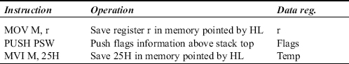
The data sent out from a register during a MW machine cycle depends on the MW machine cycle within an instruction as shown below. Here, ‘r’ stands for any of the registers A, B, C, D, E, H, or L.
| r | Saving register r in memory pointed by HL in ‘MOV M, r’ |
| Flags | Pushing information above stack top in ‘PUSH PSW’ |
| Temp | Saving of 25H in memory pointed by HL in ‘MVI M, 25H’ |
The address sent out from a register pair in a MW machine cycle depends on the MW machine cycle within an instruction as shown in the following.

The data sent out from a register during a MW machine cycle depends on the MW machine cycle within an instruction as shown in the following. Here, ‘r’ stands for any of the registers A, B, C, D, E, H, or L.
Execution of STA D525H instruction. Let us say, at location C004H, we have 32H, which is the opcode for the instruction ‘STA a16’. This instruction needs 13 clock cycles for the OF, decode, and execution. It uses an OF machine cycle of four clocks, followed by two MR and a MW machine cycle, each of three clocks. The action performed by the 8085 in these 13 clock cycles is explained in the following discussion.
In the first three clock cycles, 32H will be received in IR register from memory location C004H. The decoding is done in T4 state. The control unit understands that the opcode corresponds to the 3-byte instruction whose mnemonic is STA. These four T states constitute the OF machine cycle, described earlier. In the meanwhile, PC contents would have been incremented to C005H.
As the control unit understands that STA instruction is 3-bytes long, it decides to fetch from the next two memory locations the second and third bytes of the instruction. The 8085 performs a MR machine cycle by sending out the PC value of C005H, and by receiving 25H in the Z register. This MR operation takes three clocks as described earlier. In the meanwhile, PC contents would have been incremented to C006H.
The 8085 then performs another MR machine cycle by sending out the PC value of C006H, and by receiving D5H in the Wregister. This MR operation takes another three clocks. In the meanwhile, PC contents would have been incremented to C007H.
Only now the control unit has understood that the instruction to be executed is STAD525H. The control unit understands that for instruction execution, contents of the accumulator should be stored in memory location whose address is present in WZ pair. This is performed in a MW machine cycle using three clock cycles. If the Accumulator has the value 25H, then contents of D525H will change to 25H. As this is a MW machine cycle, PC value remains unaltered at C007H.
Fig. 13.11 depicts OF, decode, and execution of STA D525H instruction in a simple way. In this figure, the original content of D525H is shown as 52H.

Fig. 13.11 Illustrating ‘STA D525H’ instruction execution
Example 5
Execution of PUSH PSW instruction. Let us say, at location C007H, we have F5H, which is the opcode for the instruction PUSH PSW. This instruction needs 12 clock cycles for the OF, decode, and execution. It uses an OF machine cycle of six clocks, followed by two MW machine cycles, each of three clocks. The action performed by the 8085 in these 12 clock cycles is explained in the following.
In the first three clock cycles, F5H will be received in the IR register from memory location C007H. The decoding is done in T4 state. The control unit understands that the opcode corresponds to the single-byte instruction whose mnemonic is PUSH PSW. In the meanwhile, PC contents would have been incremented to C008H. In the next two clock cycles of this OF machine cycle, SP value will be decremented by 1. These six T states constitute the OF machine cycle in this case.
By the end of the T4 state in the OF machine cycle, 8085 understands that for instruction execution, contents of the Accumulator and the Flags register should be stored above the stack top. Suppose SPcontent is C708H, Accumulator content is 30H, and Flags value is 40H, then C707H contents should change to 30H, and C706H contents should change to 40H.
To push accumulator above the stack top, first of all SP contents have to be decremented from C708H to C707H using the decrementer. This is performed in T5 and T6 states of OF machine cycle. Only then MW machine cycle begins by sending out the address C707H from SP, and the data 30H from the Accumulator. As it is a MWmachine cycle, PC value remains unaltered at C008H. However, in the meanwhile the SP value would be decremented from C707H to C706H. This MW machine cycle uses three clock cycles.
Then the next MWmachine cycle begins by sending out the address C706H from SP, and the data 40H from Flags register. As it is a MW machine cycle, PC value remains unaltered at C008H. Even SPvalue remains unaltered at C706H in this case. This MW machine cycle uses three clock cycles.
Fig. 13.12 depicts OF, decode, and execution of PUSH PSW instruction in a simple way. In this figure, the original contents of C706H and C707H are shown as 52H and 42H, respectively.

Fig. 13.12 Illustrating ‘PUSH PSW’ instruction execution
The OF machine cycle uses six T states in the following cases.
- When the instruction execution requires storing information above the stack top. Instructions in this category are PUSH rp, CALLa16, RSTn, and conditional call instructions.
- When the instruction is INX rp or DCX rp.
- When the instruction is PCHLor SPHL.
- When it is a conditional return instruction.
Example 6
Execution of OUT25H instruction. Let us say, at location C008H, we have D3H, which is the opcode for the instruction ‘OUTa8’. This It uses an OF machine cycle of four clocks, followed by a MR and an IOWmachine cycle, each of three clocks. The action performed by the 8085 in these ten clock cycles is explained in the following.
In the first three clock cycles D3H will be received in IR register from memory location C008H. The decoding is done in T4 state. The control unit understands that the opcode corresponds to the 2-byte instruction whose mnemonic is OUT. These four T states constitute the OF machine cycle. In the meanwhile, PC contents would have been incremented to C009H.
As the control unit understands that the OUT instruction is 2-bytes long, it decides to fetch the second byte of the instruction from the next memory location. The 8085 performs a MR machine cycle, by sending out the PC value of C009H, and by receiving 25H in the W register and also the Z register. The point to be noted here is that both Wand Z registers are loaded with the same value, 25H. This MR operation takes three clocks. In the meanwhile, PC contents would have been incremented to C00AH.
Only now the control unit has understood that the instruction to be executed is OUT 25H. The control unit understands that for instruction execution, contents of the Accumulator should be stored in an output port whose address is 25H. This is performed in an I/O write (IOW) machine cycle using three clock cycles.
If the Accumulator has the value D5H, then contents of the output port 25H will change to D5H. Just as with a MWmachine cycle, PC value remains unaltered at C00AH in this IOWmachine cycle. Fig. 13.13 depicts OF, decode, and execution of OUT25H instruction in a simple way. In this figure, the original content of output port 25H is shown as 52H.

Fig. 13.13 Illustrating ‘OUT 25H’ instruction execution
13.2.4 I/O WRITE (IOW) MACHINE CYCLE
The last three clock cycles in OUT 25H instruction is an example for IOW machine cycle. Waveforms for IOW machine cycle are shown in Fig. 13.14.

Fig. 13.14 Waveforms for IOW machine cycle (without wait state)
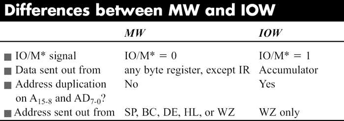
Note that in an IOW machine cycle, Wand Z will have identical 8-bit port address. There is a definite advantage because of address duplication on A15-8 and AD7-0 when using 8755 (2K × 8 EPROM and two 8-bit ports) and 8155 (combination of 256 × 8 RAM, 3 I/O ports, and 14-bit timer). A 8085-based microcomputer can be formed using only these two chips in addition to 8085. However, these chips are not in favour these days, except when minimum chip microcomputer configuration is desired.
The 16-bit value in register pair WZ will be sent out as the address in the IOW machine cycle. Also, note that in an IOW machine cycle, only the Accumulator contents will be sent out as the data to the addressed output port. In 8085, we come across IOW machine cycle only during the execution of OUT a8 instruction.
Example 7
Execution of IN 35H instruction. Let us say, at location C00AH, we have DBH, which is the opcode for the instruction ‘IN a8’. This instruction needs ten clock cycles for the OF, decode, and execution. It uses an OF machine cycle of four clocks, followed by a MR and an IOR machine cycle, each of three clocks. The action performed by the 8085 in these ten clock cycles is explained in the following.
In the first three clock cycles, DBH will be received in IR register from memory location C00AH. The decoding is done in the T4 state. The control unit understands that the opcode corresponds to the 2-byte instruction whose mnemonic is IN. These four T states constitute the OF machine cycle. In the meanwhile PC contents would have been incremented to C00BH.
As the control unit understands that IN instruction is 2-bytes long, it decides to fetch the second byte of the instruction from the next memory location. The 8085 performs a MR machine cycle by sending out the PC value of C00BH, and by receiving 35H in the W register and also the Z register. The point to be noted here is that both W and Z registers are loaded with the same value 35H. The advantage of address duplication in WZ pair in IN a8 instruction is same as that in a OUT a8 instruction. This MR operation takes three clocks. In the meanwhile, PC contents would have been incremented to C00CH.
Only now the control unit has understood that the instruction to be executed is IN 35H. The control unit understands that for instruction execution, the Accumulator should be loaded with contents of the input port whose address is 35H.
This is performed in a I/O read (IOR) machine cycle using three clock cycles. If input port 35H has the value D5H, then contents of the Accumulator will change to D5H. Just as with a IOW machine cycle, PC value remains unaltered at C00CH in this IOR machine cycle.
Fig. 13.15 depicts OF, decode, and execution of IN 25H instruction in a simple way. In this figure, the original content of the Accumulator is shown as 52H.

Fig. 13.15 Illustrating ‘IN 35H’ instruction execution
13.2.5 I/O READ (IOR) MACHINE CYCLE
The last three clock cycles in IN 35H instruction is an example for IOR machine cycle. Waveforms for IOR machine cycle areshown in Fig. 13.16.
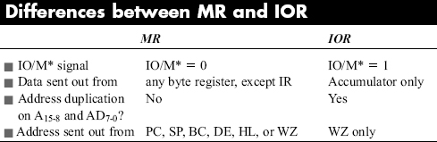
Note that in an IOR machine cycle, Wand Z willhave identical 8-bit port address. The 16-bit value in register pair WZ will be sent out as the address in an IOR machine cycle. Also, note that in an IOR machine cycle, only the Accumulator receives the data from the addressed input port. In 8085, we come across IOR machine cycle only during the execution of IN a8 instruction.

Fig. 13.16 Waveforms for IOR machine cycle (without wait state)
13.3 COMPARISON OF DIFFERENT MACHINE CYCLES
So far we have come across OF, MR, MW, IOR, and IOW machine cycles. The other possible machine cycles in 8085 are BI (bus idle) and INA (interrupt acknowledge) machine cycles. They will be discussed in the chapter on 8085 interrupts. Now the differences between some of the machine cycles are presented in the following tables.


13.4 MEMORY SPEED REQUIREMENT
At the end of the T2 state in a machine cycle, 8085 senses the Ready input pin. If it is logic 0, 8085 enters Twait state, else it enters the T3 state. The Ready input is permanently tied to logic 1, if the memory chips and the I/O ports in the system are having compatible speed with 8085. Otherwise, appropriate number of wait states has to be generated by external circuitry. Infact, in the ALS kit the Ready pin is tied to logic 1. But then, how to conclude whether the memory chips are having compatible speeds or not? That is the topic of this section.
As an example, let us check up if the 27128A-20 16K×8 EPROM chip can be used without any wait states with a 8085 operating at 320 nS clock period. For interfacing a memory chip, the most important timing parameters to be considered are tcc, tCE, and tOE. The memory read timing for a typical EPROM chip is shown in Fig. 13.17.
For 27128A-20 chip, the characteristics are as follows.
tAcc = 200 nS max
tCE = 200 nS max
tOE = 75 nS max

Fig. 13.17 Memory read timing for 27128A-20 16K×8 EPROM
tAcc = 200 nS means that, it takes a maximum of 200 nS to output the data after stable address is received by the 27128, under the following assumptions.
- The memory chip would have been selected atleast 200 nS (tCE) before the data is output by it
- The output enable line of the memory chip would have been activated atleast 75 nS (tOE)before the data is output by it.
tCE = 200 nS means that, it takes a maximum of 200 nS to output the data after the 27128 has been selected, under the following assumptions.
- The memory chip would have received stable address atleast 200 nS(tAcc) before the data is output by it.
- The output enable line of the memory chip would have been activated atleast 75 nS (tOE)before the data is output by it.
Generally address and chip select signals are received by a memory chip at about the same time. Of course, there will be some time difference depending on the propagation delays of the chips between the microprocessor and the memory chip.
tOE = 75 nS means that, it takes a maximum of 75 nS to output the data after the 27128 output has been enabled, under the following assumptions.
- The memory chip would have received stable address atleast 200 nS(tAcc) before the data is output by it.
- The memory chip would have been selected atleast 200 nS (tCE) before the data is output by it.
Generally, it is the read signal that enables the output buffers of a memory chip to output the data. This signal isactivated a little while after the address and chip select signals are received by the chip. The 27128 chip needs a maximum of 75 nS to output the data after the output of the chip is enabled.
The bus timing characteristics of MR machine cycle is shown in Fig. 13.18. The important parameters to be considered are tAD, tLDR, and tRD. tAD is the time interval between valid address on A15-0 and valid data on AD7-0. tLDR is the time interval between trailing edge of ALE and valid data on AD7-0 during a read operation. tRD is the time interval between leading edge of RD* and valid data on AD7-0.

Fig. 13.18 Bus timing characteristics of MR machine cycle
The maximum values of these parameters in nanoseconds, as provided byIntel manuals, for 8085AH and 8085AH-2 are as shown in the following. In this table, T stands for cycle time and N stands fornumber of wait states.

If we assume that there are no wait states, and T value as 320 nS (3.125 MHz) for 8085AH, and 200 nS (5 MHz)for 8085AH-2, we get maximum values of these parameters as:

The other important parameters to be considered are tAL, tAC, and tLC. tAL is the time interval between valid address on A15-0 and trailing edge of ALE. tAC is the time interval between valid address on AD15-0 and leading edge (1 to 0 transition) of RD* control signal during a read operation. tLC is the time interval between trailing edge (1 to 0 transition) of ALE and leading edge of RD* control during a read operation.
The minimum values of these parameters in nanoseconds, as provided by Intel manuals, for 8085AH and 8085AH-2 are indicated as follows.

If we assume T value as 320 nS (3.125 MHz) for 8085AH, and 200 nS (5 MHz) for 8085AH-2, we get minimum values of these parameters as:

The other useful parameter to be considered is tCC. It is the width of the RD* control signal in the logic 0 state during a read operation. The minimum value of this parameter in nanoseconds, as provided by Intel manuals, for 8085AH and 8085AH-2 are as shown.
| 8085AH | 8085AH-2 |
| tCC(1.5+N)T-80 | (1.5+N)T-70 |
If we assume that there are no wait states, and T value as 320 nS (3.125 MHz) for 8085AH, and 200 nS (5 MHz)for 8085AH-2, we get minimum value of this parameter as:
| 8085AH | 8085AH-2 |
| tCC400 nS 230 nS |
The 8085 reads the data on the AD7-0 lines when RD* makes 0 to 1 transition. Thus maximum value of tAD should be ideally tAC + tCC. So for 8085AH working at 320 nS, maximum value of tADshould be 270 nS + 400 nS = 670 nS. But practically, the data should be present on AD7-0 some time before the 0 to 1 transition of RD* signal. Thus Intel manuals specify a maximum value of 575 nS for tAD when 8085AH is working at 320 nS.
Similarly, maximum value of tLDR should be ideally tLC + tCC. So for 8085AH working at 320 nS, maximum value of tLDR should be 130 nS + 400 nS = 530 nS. But practically, the data should be present on AD7-0 some time before the 0 to 1 transition of RD* signal. Thus Intel manuals specify a maximum value of 460nS for tLDR when 8085AH is working at 320 nS.
Similarly, maximum value of tRD should be ideally tCC. So for 8085AH working at320 nS, tRD should be 400 nS. But practically, Intel manuals specify a maximum value of 300 nS for tRDwhen 8085AH is working at 320 nS.
Fig. 13.19 shows the actual interfacing details of 27128A-2 chip in the ALS kit. Using this figure and figures 13.17 and 13.18, we can assess the compatibility of this chip with 8085AHworking with 320-nS clock period.
We start the calculations assuming that stableaddress and IO/M* signals are sent out by the 8085AH at time 0 nS. Then, ALE goes to 0 state at 115 nS (tAL), and RD* isactivated at 270 nS (tAC).
13.4.1 EARLIEST DATA OUTPUT TIME CONSIDERING tACC
Address A13-8 is received by the 27128 from 8085AH via 74LS244 octal line driver, which has a propagation delayof 12 nS. Address A7-0 is received by the 27128 from 8085AH via 74LS373 octal latch,which has a propagation delay of 30 nS. Thus, address A13-0is received by 27128 at the end of 30 nS. Thus, the data can only comeout on D7-0 pins of 27128 by 30 nS + tAcc = 30nS + 200nS = 230 nS.

Fig. 13.19 Delays involved in accessing 27128 EPROM in ALS kit
13.4.2 EARLIEST DATA OUTPUT TIME CONSIDERING tCE
The 74138 receives A15-14 from 8085 via 74LS244 (octal line driver, with 12-nS delay). It simultaneously receives IO/M* signal from 8085 via 74LS244 (octal line driver, with delay of 12 nS). Then CS* signal is received by the 27128 from 74LS138 (3 to 8 decoder, with delay of 22 nS). Thus, CS* signal is received by 27128 at the end of 34 nS. Thus, the data can only come out on D7-0 pins of 27128 by 34 nS + tCE = 34 nS + 200 nS = 234 nS.
13.4.3 EARLIEST DATA OUTPUT TIME CONSIDERING tOE
The 8085AH activates RD* signal at 270 nS. This signal goes to OE* pin of 27128 via 74LS241 (octal line driver, with 12nS delay). Thus, OE* signal is received by 27128 at the end of 282 nS. Thus, the data can only come out on D7-0 pins of 27128 by 282 nS + tOE = 282 nS + 75 nS + 357 nS.
From the discussion in the previous three paragraphs, it should be clear that the earliest data output time will be357 nS, considering all the three parameters tACC, tCE, and tOE. In fact, tAcc can be as large as 200nS + (357nS – 230nS) = 327nS, without affecting the time at which data comes out of memory chip. Similarly tCE can be as large as 200 nS + (357 nS – 234nS) = 323nS, without affecting the time at which data comes out of the memory chip.
The 8085AH receives this data from 27128 via 74LS245 (octal bus transceiver, with delay of 8 nS). Thus, valid data is received by the 8085AH at 357 nS + 8 nS = 365 nS.
13.4.4 27128-20 COMPATIBILITY CHECK wITH 8085AH
Now let us perform memory compatibility check with respect to the parameters tAD, tLDR, and tRD.
Compatibility with respect to tAD:tAD is the time interval between valid address on A15-0 and valid data on AD7-0. For 8085AH workingwith a T state of 320 nS, it is a maximum of 575 nS. But in this case, the valid data is available in 365 nS itself. Thus the memory speed is compatible, with actually an excess time margin of 575 nS - 365 nS = 210 nS.
Compatibility with respect to tLDR:tLDR is the time interval between trailing edge of ALE and valid data on AD7-0 during a read operation. For 8085AH working with a T state of 320 nS, it is a maximum of 460 nS. The trailing edge of ALE occurs at 115 nS. Thus tLDR in this case is only 365 nS - 115 nS = 250 nS. Thus, thememory speed is compatible, with actually an excess time margin of 460 nS = 250 nS = 210 nS.
Compatibility with respect to tRD: tRD is the time interval between leading edge of RD* and valid data on AD7-0. For 8085AH working with a T state of 320 nS, it is a maximum of 300 nS. The 8085AH activates RD* signal at 270 nS and the valid data is available by 365 nS itself. Thus tRD in this case is only 365 nS - 270 nS = 95nS. Thus, the memory speed is compatible with actually an excess timemargin of 300 nS - 95 nS = 205 nS.
Thus, 27128-20 EPROM chip is speed compatible with 8085AH. In fact, as per the discussion in the previous three paragraphs, there is an excess time margin of atleast 205 nS. Thus, the 8085AH can be interfaced with memory chips, which have the worst case specifications as shown in the following.
tAcc = 327 nS + 205 nS = 532 nS
tCE = 323 nS + 205 nS = 528 nS
tOE = 75 nS + 205 nS = 280 nS
In this case, as discussed in section (13.4.3), 327 nS is the largest tAcc possible without affecting the time (357 nS) at which the data comes out of memory chip. Corresponding values for tCE and tOE are 323 nS and 75 nS respectively. 205 ns in the margin still available when 8085AH is interfaced with memory chips.
13.4.5 ASSESSING COMPATIBILITY OF 27128-20 WITH 8085AH-2
The 8085AH-2 works with 200nS clock period. We start the calculations assuming that valid address, and IO/M* signals are sent out by the 8085AH-2 at time 0 nS. Then, ALE goes to 0 state at 50 nS (tAL), and RD* is activated at 115 nS (tAC).
Earliest data output time considering tAcc: Address A13-18 is received by the 27128 from 8085 via 74LS244 (octal line driver, with delay of 12 nS). Address A7-0 is received by the 27128 from 8085 via 74LS373 (octal latch, with delay of 30 nS). Thus, address A13-0 is received by 27128 at the end of 30 nS. Thus, the data can only come out on D7-0 pins of 27128 by 30 nS + tAcc = 30 nS + 200 nS = 230 nS.
Earliest data output time considering tCE:The 74138 receives A15-14from 8085 via 74LS244 (octal line driver, with 12 nS delay). It simultaneously receives IO/M* signal from 8085 via 74LS241 (octal line driver, with delay of 12 nS). Then CS* signal is received by the 27128 from 74LS138 (3 to 8 decoder, with delay of 22 nS). Thus, CS* signal is received by 27128 at the end of 34 nS. Thus, the data can only come out on D7-0 pins of 27128 by 30 nS + tCE = 34 nS + 200 nS = 234 nS.
Earliest data output time considering tOE: The 8085AH-2 activates RD* signal at 115 nS. This signal goes toOE* pin of 27128 via 74LS241 (octal line driver, with 12 nS delay). Thus, OE* signal is received by 27128 at the end of 127 nS. Thus, the data can only come out on D7-0 pins of 27128 by 127 nS + tOE = 127 nS + 75 nS = 202 nS.
From the discussion in the previous three paragraphs, it should be clear that the earliest data output time will be 234 nS, considering all the three parameters tACC, tCExy, and tOE. In fact, tAcc can beas large as 200 nS + (234 nS - 230 nS) = 204 nS, without affecting the time at which data comes out of memory chip. Similarly tOE can be as large as 75 nS + (234 nS - 202 nS) = 107 nS, without affecting the time at which data comes out of memory chip.
The 8085AH-2 receives this data from 27128 via 74LS245 (octal bus transceiver with delay of 8 nS). Thus, valid data is received by the 8085AH-2 at 234 nS + 8nS = 242 nS.
Now let us perform memory compatibility check with respectto the parameters tAD, tLDR, and tRD.
Compatibility with respect to tAD: For 8085AH-2 working with a T state of 200 nS, it is a maximum of350 nS. But in this case, the valid data is available in 242 nS itself. Thus the memory speed is compatible with actually an excess time margin of 350 nS - 242 nS = 108 nS.
Compatibility with respect to tLDR: For 8085AH-2 working with a T state of 200 nS, it is a maximum of 270 nS. The trailing edge of ALE occurs at 50 nS. Thus tLDR in this case is only 242 nS - 50 nS = 192 nS. Thus, the memory speed is compatible, with actually an excess time margin of 270nS - 192 nS = 78 nS.
Compatibility with respect to tRD: For 8085AH-2 working with a T state of 200 nS, it is a maximum of150 nS. The 8085AH-2 activates RD* signal at 115 nS and the valid data is available by 242 nS itself. Thus, tRD in this case is only 242 nS – 115 nS = 127 nS. Thus, the memory speed is compatible, with actually an excess time margin of 150 nS – 127 nS = 23 nS.
Thus, 27128-20 EPROM chip is speed compatible with 8085AH-2 also. In fact, as per the discussion in the previous three paragraphs, there is an excess time margin of atleast 23 nS. Thus, the 8085AH-2 can be interfaced with memory chips, which have the worst case specifications indicated as follows:
tACC = 204 nS + 23 nS = 227 nS
tCE = 200 nS + 23 nS = 223 nS
tOE = 107 nS + 23 nS = 130 nS
In this case, 204 nS is the largest tAcc possible without affecting the time (234 nS) at which the data comes out of memory chip. Corresponding values for tCE and tOE are 200 nS and 107 nS respectively.23 ns in the margin still available when 8085AH-2 is interfaced with memory chips.
13.5 WAIT STATE GENERATION
The present day memory and peripheral chips are fast enough for a 8085 working at 3 MHz. So wait states are generally not needed at all. If 8085AH-2 is used, which can work at 5 MHz, there may be a need to insert one wait state, between T2 and T3. The circuit shown in Fig. 13.20 easily achieves this.
The circuit uses two D-type positive edge-triggeredflip flops, with active low Reset inputs. At the beginning of T1, ALE goeshigh and causes Q1 to go high. As Q1 and D2 are connected, D2 remains highthroughout T1. The positive edge of T2 clock causes Q2* to become 0. This is connected to ready input of 8085. Thus, ready input remains 0 throughout the T2 state. So 8085 enters Twait, instead of T3, after T2. Also, when Q2* becomes 0, Reset1* becomes 0, thus making Q1 output as 0 throughout T2 state. The positive edge of Twait causes Q2* to become 1. This makes ready input as 1, andso after Twait state, 8085 enters the T3 state. Thus, one wait state is inserted by the circuit in Fig. 13.20 between T2 and T3. This can be visualized from the waveforms indicated in Fig. 13.21.

Fig. 13.20 Circuit to insert a wait state between T2 and T3

Fig. 13.21 Waveforms indicating generation of wait state
- What is the difference between the programmer's view of 8085 and architecture of 8085?
- With a neat diagram explain the architecture of 8085 needed for instruction execution.
- Explain the role of IR, Temp, W and Z registers in the architecture of8085.
- Indicate with reason, whether the following registers are connected tothe internal bus in a unidirectional or bi-directional way.
- Accumulator
- Temp
- IR
- Flags
- W
- D
- Mention the steps involved in an instruction cycle and explain the steps with an example.
- Explain the terms clock cycle (T state), machine cycle, and instruction cycle.
- List the machine cycles, the registers involved, and the total number of clock cycles needed in the fetching and execution of the following instructions (check your answer with the information provided in the appendix).
- MVI B, 25H;
- STAX D;
- LXI B, 1234H;
- XRA B;
- JNC 1234H;
- CALL 1234H;
- DAD D;
- POP B;
- RST 5;
- PCHL;
- XTHL;
- SPHL;
- XCHG;
- RNC;
- SHLD 1234H;
- OUT 25H.
- Give two examples for each of the following.
- Instructions that need only OF with 4 T states ;
- Instructions that need only OF with 6 T states ;
- Instructions that need OF and MR;
- Instructions that need OF, MR, and MR;
- Instructions that need OF, MR, and MW.
- Give atleast one example for each of the following.
- Instructions that need OF, MR, MR, MW, and MW;
- Instructions that need OF, MR, and IOR;
- Instructions that need OF, BI, and BI;
- Instructions that need OF, MW, and MW.
- Compare the following machine cycles.
- OF with MR;
- MR with IOR;;
- MW with IOW.
- Explain the terms tAcc, tCE, and tOE for a memory chip.
- Explain the following terms with reference to a MR cycle.
- tAD;
- tLDR;
- tRD;
- tAL;
- tAC;
- tLC.
- Suppose a memory chip has the following specifications.
- tAcc = 350 nS
- tCE = 360 nS
- tOE = 180 nS
Can this chip be interfaced with (assume interface circuit of Fig. 13.19):
- 8085AH with a T state of 350 nS?
- 8085AH-2 with a T state of 220 nS?
- Calculate the number of wait states needed if 8085AH-2 working with a T state of 200 nS is required to be interfaced with a memory chip having the following specifications. Assume interface circuit of Fig. 13.19.
- tAcc = 550 nS
- tCE = 500 nS
- tOE = 220 nS
- Explain with a neat diagram a circuit to insert one wait state between T2 and T3 states in a machine cycle.