
12
Addressing of I/O Ports
![]() Need for I/O ports
Need for I/O ports
![]() Comparison of I/O port chips and memory chips
Comparison of I/O port chips and memory chips
![]() IN and OUT instructions
IN and OUT instructions
![]() IN a8 instruction
IN a8 instruction
![]() OUT a8 instruction
OUT a8 instruction
![]() Memory-mapped I/O
Memory-mapped I/O
![]() I/O-mapped I/O
I/O-mapped I/O
![]() Comparison of memory-mapped I/O and I/O-mapped I/O
Comparison of memory-mapped I/O and I/O-mapped I/O
![]() Merits of I/O-mapped I/O and demerits of memory-mapped I/O
Merits of I/O-mapped I/O and demerits of memory-mapped I/O
![]() Demerits of I/O-mapped I/O and merits of memory-mapped I/O
Demerits of I/O-mapped I/O and merits of memory-mapped I/O
![]() I/O-mapped I/O or memory-mapped I/O
I/O-mapped I/O or memory-mapped I/O
![]() Questions
Questions
This chapter reverts to the description of instruction types. Two of the remaining 7 instruction types are explained here. This chapter discusses in detail the importance and need for I/O ports and also describes memory-mapped I/O and I/O-mapped I/O.
 12.1 NEED FOR I/O PORTS
CPU and main memory are very fast compared with electromechanical input or output devices like printers, etc. In such a case, it is essential that the data lines of the computer are not kept engaged for a long time during communication with input/output (I/O) devices. Otherwise, the overall speed of the computer system comes down drastically. So I/O devices are connected to a computer through I/O ports.
For example, to communicate with a printer, the CPU loads the output port connected to the printer at electronic speeds. The printer slowly prints this. When the printer has finished printing, the output port requests the CPU for further data. This way, the CPU is allowed to work at its full speed, with no degradation in the overall speed of the computer system.
In fact, to further improve the speed, a printer will have printer buffer. For example, the popular LX-800 Epson dot matrix printer has a printer buffer size of 3 KB. The microcomputer fills this buffer in a fraction of a second. Then as far as the computer is concerned the printing is over! But, the user would not have witnessed the printing of a single character as yet! The printer prints this entire information in about 15-20 s. Then the printer requests for further data to be printed, from the computer.
Thus I/O devices are never directly connected to a computer. Computer and an I/O device always communicate with an I/O port as the middleman.
12.1.1 COMPARISON OF I/O PORT Chips AND MEMORY CHIPS
An I/O port chip also stores information like a memory chip. But, an I/O port chip generally stores only 1 byte of information, and some I/O port chips store a few bytes of information. For example, Intel 8212 I/O port chip stores only 1 byte of information, but Intel 8255 chip can be used to store 3 bytes of information. However, memory chips contain a large number of memory locations like 1K, 4K, 8K, etc. A location within a memory chip is selected by the address pins An-0.
Second, an I/O port chip will have eight lines for communication with the microprocessor, and another eight lines for communication with the I/O device. An I/O port only acts as a buffer between the microprocessor and the I/O device. But, a memory chip will have only eight lines for communication with the microprocessor.
Third, many I/O port chips are programmable. That is, the user can decide the way the I/O port should work in his system. An example for a programmable I/O port chip is Intel 8255. In this case, the user can program a port as an input port or an output port. Also, the user can program a port to work in one of the several modes like basic I/O, handshake I/O, etc. However, there are I/O port chips, which are non-programmable. An example is Intel 8212. Obviously, programmable I/O ports are more popular than non-programmable ports. But memory chips are only storage chips, and as such are not programmable.
Fig. 12.1a, b, and c indicate the essential pins needed in an output port, an input port, and a memory chip. For simplicity, I/O port chip with a single port is shown.
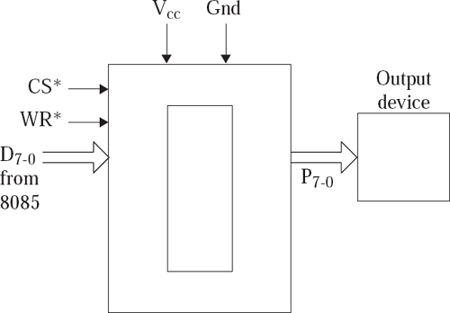
Fig. 12.1a Pins for an output port chip

Fig. 12.1b Pins for an input port chip

Fig. 12.1c Pins for a memory chip
12.2 IN AND OUT INSTRUCTIONS
There are two instructions in 8085 for communication with I/O ports. They are the IN and OUT instructions. The IN or OUT instruction mnemonic should be followed by an 8-bit port address. Thus 28 = 256 input ports and 256 output ports are possible in a 8085-based microcomputer.
12.2.1 IN a8 INSTRUCTION
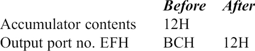
IN is a mnemonic that stands for INput to Accumulator from the contents of input port whose 8-bit address is indicated in the instruction as a8. It occupies 2 bytes in memory. The first byte specifies the opcode, and the next byte provides the 8-bit port address. IN EFH is an example instruction of this type. The result of execution of this instruction is shown below with an example.

IN instruction is the only instruction using which the Accumulator can be loaded with the contents of an input port. A possible chip select circuit to connect an input port with an address as EFH is as shown in Fig. 12.2.
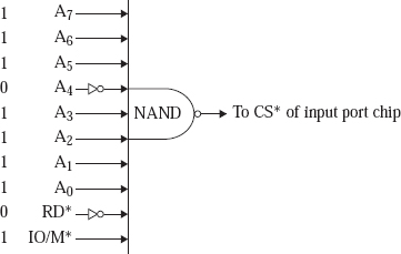
Fig. 12.2 Chip select circuit for input port EFH
Notice that when A7 A6 A5 A4 A3 A2 A1 A0 = 1 1 1 0 1 1 1 1, RD* = 0, and IO/M* = 1, all the inputs to the Nand gate become logic 1, and so the input port chip gets selected. Thus the chip responds when the 8085 sends out address as EFH, IO/M* as 1, and RD* as 0. In other words, we can say that it is input port number EFH.
Summary: IN a8 (2 bytes; IN EFH; 1 opcode)
12.2.2 OUT a8 INSTRUCTION
OUT is a mnemonic that stands for OUTput Accumulator contents to an output port whose 8-bit address is indicated in the instruction as a8. It occupies 2 bytes in memory. First byte specifies the opcode, and the next byte provides the 8-bit port address. OUT EFH is an example instruction of this type. The result of execution of this instruction is shown below with an example.
OUT instruction is the only instruction using which Accumulator contents can be sent out to an output port. A possible chip select circuit to connect an output port with an address as EFH is as shown in Fig. 12.3.
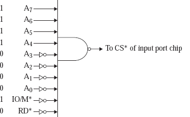
Fig. 12.3 Chip select circuit for output port EFH
Notice that when A7 A6 A5 A4 A3 A2 A1 A0 = 1 1 1 0 1 1 1 1, WR* = 0, and IO/M* = 1, all the inputs to the Nand gate become logic 1, and so the output port chip gets selected. Thus, the chip responds when the 8085 sends out address as EFH, IO/M* as 1, and WR* as 0. In other words, we can say, it is output port number EFH.
Notice that it is possible to have an input port with the address EFH, and an output port with the same address EFH. When the 8085 sends out the address as EFH and IO/M* as 1, only one of them is selected based on the RD* and WR* signals. Thus, it is possible to have a total of 256 input ports and a total of 256 output ports.
Summary: OUT a8 (2 bytes; OUT EFH; 1 opcode)
12.3 MEMORY-MAPPED I/O
It is possible to address an I/O port as if it were a memory location. For example, let us say, the chip select pin of an I/O port chip is activated when address = FFF0H, IO/M* = 0, and RD* = 0. This is shown in Fig. 12.4.
In this case, the I/O port chip is selected when the 8085 is thinking that it is addressing memory location FFF0H for a read operation. Note that 8085 thinks that it is addressing a memory location because it has sent out IO/M* as a logic 0. But in reality, an input port has been selected, and the input port supplies information to the 8085. Such I/O ports that are addressed by the processor as if they were memory locations are called memory-mapped I/O ports.
Fig. 12.4 Memory-mapped input port with address FFF0H
12.4 I/O-MAPPED I/O
Generally, a processor like 8085 addresses an I/O port by sending out 8-bit port address and IO/M* = 1. For example, let us say, the chip select pin of an I/O port chip is activated when 8-bit address = F0H, IO/M* = 1, and RD* = 0. This is shown in Fig. 12.5.
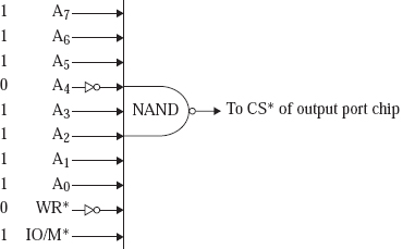
Fig. 12.5 I/O-mapped input port with address F0H
Such I/O ports, which are addressed by the processor by sending out IO/M* as logic 1 are called I/O-mapped I/O ports. Our discussion about I/O ports in Sect. 12.2 of this chapter was confined to only such I/O-mapped I/O ports.
12.5 COMPARISON OF MEMORY-MAPPED I/O AND I/O-MAPPED I/O
In this section the merits and demerits of these two schemes of addressing of I/O ports is discussed.
12.5.1 MERITS OF I/O-MAPPED I/O AND DEMERITS OF MEMORY-MAPPED I/O
- IN and OUT instructions are used for addressing I/O-mapped I/O ports. The mnemonics of these instructions clearly indicate that the processor communicates with an I/O port. To load accumulator from memory-mapped input port with address FFF0H, we have to execute LDA FFF0H instruction. The mnemonic of this instruction gives the impression that the accumulator is being loaded from memory location FFF0H!
- Some microprocessors have a control pin to select a memory location or an I/O port. For example, in 8085, IO/M* pin is used to select an I/O port or a memory location. The address sent out on the address pins selects an I/O port or a memory location based on the value sent out on IO/M*. In other words, there are two separate address spaces-one for I/O ports and another for memory, as shown in Fig. 12.6.

Fig. 12.6 Memory address space and I/O address space for 8085
- The I/O address space has only 256 locations, as I/O port addresses are only 8 bits in size in 8085. The memory address space has 64K locations, as memory addresses are 16-bits long in 8085. Thus it is possible to have full 64K space exclusively for memory, if we prefer to use I/O-mapped I/O scheme for addressing I/O ports. It is possible to have an I/O-mapped I/O port with the address 67H, and also have a memory location with the address 0067H.
- If we connect I/O ports as memory-mapped ports with addresses in the range of FF00H-FFF0H, then we should not allot this address range to any memory chip. If memory and a memory-mapped I/O port have the same address, both get selected simultaneously, and this can damage the processor, the memory chip, and the I/O port chip. Thus with memory-mapped I/O, the entire 64K address space (in case of 8085) is not available for memory. This is because some address space is lost to memory-mapped I/O ports.
12.5.2 DEMERITS OF I/O-MAPPED I/O AND MERITS OF MEMORY-MAPPEDI/O
- Only IN and OUT instructions are used for addressing I/O-mapped I/O ports. But a large number of instructions can be used for communication with a memory-mapped I/O port. In fact, all the instructions that can be used to access a memory location can be used to access a memory-mapped I/O port. Suppose we have a memory-mapped input port with the address FFF0H, then the effect of executing the following instructions is shown alongside in the comments field.
LXI H, FFF0H; HL pair loaded with FFF0H MOV C, M ; C register loaded with contents of input port FFF0H INR M ; Increment by 1 contents of input port FFF0H ANA M ; Perform AND of accumulator and input port FFF0H ADD M ; Add accumulator contents and input port FFF0H - The designer of a microprocessor is required to produce a chip design with minimum possible pins. That is the reason we find multiplexed address and data pins, AD7-0. If I/O-mapped I/O facility is needed, then there must be a pin of the kind IO/M*, to distinguish between I/O addressing and memory addressing. However, if it is decided by the designer of the processor chip that memory and I/O ports will be addressed in the same way, then there is no need of IO/M* pin at all. In Motorola microprocessor chips, there is no IO/M* pin because they use memory-mapped I/O ports. In Motorola 6800 there will be a single address space in which space allocation is made for memory and I/O ports, as shown in Fig. 12.7. The ports are always memory-mapped in Motorola 6800.
- Using I/O-mapped I/O, only accumulator can communicate with an I/O port. But using memory-mapped I/O any register can communicate with a memory-mapped I/O port. For example, ‘MOV C, M’ can be used to load C register with contents of a memory-mapped I/O port, whose address is provided in HL pair.
- Using I/O-mapped I/O, only data transfer operation is possible between accumulator and an I/O port. They are done using the IN and OUT instructions. But using memory mapped I/O, even arithmetic and logical operations can be performed. For example, ADD M can be used to add accumulator and contents of a memory-mapped I/O port, whose address is provided in HL pair. Similarly, ANA M can be used perform AND operation on accumulator and contents of a memory-mapped I/O port, whose address is provided in HL pair.

- Using I/O-mapped I/O, only 256 input ports and 256 output ports could be addressed in a 8085 system, as an I/O port address is only 8-bits wide. But, using memory-mapped I/O, even upto 64K I/O ports can be addressed in a 8085 system, as memory addresses are 16-bits wide. However, this will be at a cost of corresponding reduction in memory addressing capacity.
12.5.3 I/O-MAPPED I/O OR MEMORY-MAPPED I/O?
After the previous discussion, it is not possible to conclude as to which scheme of addressing I/O ports is better. Both have their merits and demerits. Intel family of microprocessors like 8085, 8086, 80386, Pentium, and Zilog family of microprocessors like Z-80, Z-8000, etc. provide I/O-mapped I/O facility, in addition to providing memory-mapped I/O. So some I/O ports can be connected as I/O-mapped I/O ports, and some others as memory-mapped I/O ports in an Intel processor-based system. But Motorola family of microprocessors like 6800, 68000, 68020, etc. provide only memory-mapped I/O. Thus, we can say that an Intel processor is better compared with a Motorola processor, as far as addressing of I/O ports is concerned.
- Describe the need for I/O ports in a microcomputer system.
- Compare I/O port chips with memory chips.
- How many input ports and output ports are possible in 8085-based microcomputer, if the system uses only I/O-mapped I/O?
- Explain clearly what a memory-mapped I/O port means.
- With a neat circuit diagram indicate a possible chip select circuit needed to have the address of an I/O-mapped I/O port as E7H.
- With a neat circuit diagram indicate a possible chip select circuit needed to have the address of a memory-mapped I/O port as 7FE7H.
- Bring out the merits and demerits of I/O-mapped and Memory-mapped I/O.