
26
Intel 8251A—Universal Synchronous Asynchronous Receiver Transmitter (USART)
![]() Need for a USART
Need for a USART
![]() Asynchronous transmission
Asynchronous transmission
![]() Asynchronous reception
Asynchronous reception
![]() Synchronous transmission
Synchronous transmission
![]() Synchronous reception
Synchronous reception
![]() Description of 8251 USART
Description of 8251 USART
![]() Programming the 8251
Programming the 8251
![]() Mode instruction
Mode instruction
![]() Command instruction
Command instruction
![]() Identifying the command in the control port
Identifying the command in the control port
![]() Status port of 8251
Status port of 8251
![]() Use of sod pin of 8085 for serial transfer
Use of sod pin of 8085 for serial transfer
![]() Questions
Questions
This chapter deals in depth with Intel 8251A, which is a universal synchronous asynchronous receiver transmitter (USART). The 8251A is given the name USART for its capability to virtually support any serial data format. This chapter gives a detailed description of the topics mentioned in the chapter outline with neat diagrams.
 26.1 NEED FOR USART
A USART is also called a programmable communications interface (PCI). When information is to be sent by 8085 over long distances, it is economical to send it on a single line. In 8085, SOD pin can be used for this purpose, but then the 8085 has to convert 8-bit parallel data to serial data and then]output it on SOD pin. Thus lot of CPU time is required for such a conversion. A program to send out serial data on SOD pin is provided at the end of the chapter.
Similarly, if 8085 receives serial data over long distances on SID pin, the 8085 has to internally convert this into parallel data before processing it. Again, lot of time is required for such a conversion. The 8085 can delegate the job of conversion from serial to parallel and vice versa to the 8251A USART used in the system. The 8251A converts the parallel data received from the processor on the D7-0 data pins into serial data, and transmits it on TxD (transmit data) output pin of 8251. Similarly, it converts the serial data received on RxD (receive data) input into parallel data, and the processor reads it using the data pins D7-0.
In this book, 8251A will henceforth be referred to as 8251 for simplicity. The 8251 can support virtually any serial data format, and hence the name ‘universal’ synchronous asynchronous receiver transmitter. Thus there are specialized I/O port chips that can be assigned some specific tasks, instead of implementing them by software. Implementation by hardware is always much faster too and the processor is free to concentrate on those tasks, which can be taken up by the processor alone. Some of the specialized I/O port chips and their corresponding functions are indicated as follows.
- Intel 8259—Programmable interrupt controller;
- Intel 8257—Programmable DMA controller;
- Intel 8253—Programmable interval timer;
- Intel 8279—Programmable keyboard and display controller;
- Intel 8251—USART.
26.2 ASYNCHRONOUS TRANSMISSION
As the 8251 is used for communication purpose, it is necessary to study the various types of communications. In asynchronous transmission mode, the transmission of characters is not at regular intervals. The transmission is not synchronized with a clock.
The parallel data, to be transmitted in serial format, is sent by the processor to the transmit buffer of 8251. The transmit buffer is an 8-bit port that can only be written, but not read, by the processor. The processor writes to the transmit buffer by activating the CS* input and WR* inputs of 8251, when C/D* (control/data*) input is at 0. The information in the transmit buffer is automatically transferred to transmit shift register. This register acts like a parallel-in serial-out shift register.
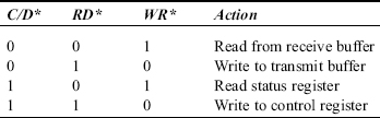
When the 8251 chip is selected, the RD*, WR*, and C/D* inputs decide which register is going to be accessed by the processor, as indicated in the following.

For the chip select circuit shown in Fig. 26.1, the 8251 is connected as an I/O-mapped I/O device. The transmit buffer and receive buffer have the same address 50H and the control and status registers have the same address 51H, as per this figure.
Intel 8251 is a programmable chip. It can be configured to suit our requirement by writing to the control port of 8251. The control port is an 8-bit port that can only be written, but not read, by the processor. The processor writes to the control port by activating the CS* and WR* inputs of 8251,
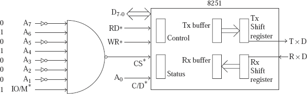
Fig. 26.1 Chip select circuit for connecting 8251 as I/O-mapped I/O
- Mode instruction (MI);
- Synchronization character or characters;
- Command instruction (CI).
Using the MI (to be described later), the 8251can be configured as indicated in the following list in the asynchronous mode for transmission as well as reception.
- 5, 6, 7, or 8 bits per character;
- Even, odd, or no parity;
- 1, 1.5, or 2 stop bits;
- ×1, ×16, or ×64 mode.
Number of Bits per Character: ASCII code is normally used for representing a character. It uses a 7-bit code. Extended ASCII code that uses 8 bits are used when some special characters like graphic characters are to be represented. Intel 8251 allows the user to specify the character length as 5, 6, 7, or 8 bits by writing appropriate information in MI.
Parity Bit: Serial communication is basically used for long distance communication. During transit, the data may get corrupted because of noise on the communication medium. The receiver of the data needs to be sure that he has received the correct data. This can be achieved to a great extent by appending a parity bit at the end of the character data. There are two types of parity bits—Odd parity and Even parity.
The bit appended at the end of the character is called odd parity bit if the number of 1s in the data including the parity bit is an odd number.
Example 1: Assume the data to be 01010010. In this, the number of 1s is 3, which is already an odd number. Thus the odd parity to be appended at the end of this character will be a 0. The character with appended odd parity bit will then be 01010010 0.
Example 2: Assume the data to be 01110010. In this, the number of 1s is 4, which is an even number. Thus the odd parity to be appended at the end of this character will be a 1, so that there may be odd number of 1s after appending the parity bit. The character with appended odd parity bit will then be 01110010 1.
The bit appended at the end of a character is called even parity bit if the number of 1s in the data including the parity bit is an even number.
Example1: Assume the data to be 01010010. In this, the number of 1s is 3, which is an odd number. Thus the even parity to be appended at the end of this character will be a 1, so that there may be even number of 1s after appending the parity bit. The character with appended even parity bit will then be 01010010 1.
Example 2: Assume the data to be 01110010. In this, the number of 1s is 4, which is already an even number. Thus the even parity to be appended at the end of this character will be a 0, so that there may be even number of 1s after appending the parity bit. The character with appended even parity bit will then be 01110010 0.
Sometimes the data is transferred in serial form over only a small distance. An examle is the downloading of the machine code of 8085 program from a personal computer to the 8085 kit using the serial port of the PC. In such a case, it may not be necessary to append a parity bit at the end of each character. This improves the speed of transmission. Intel 8251 can be programmed for appending an odd parity bit, even parity bit, or not appending any parity bit by writing appropriate information in the MI.
Start and Stop Bits: In the asynchronous mode of transmission, there can be any amount of time gap between the transmissions of two characters. Hence there is a need for the receiver to be informed about the beginning and end of the character. This is done using the start bit that is appended at the beginning of the character and stop bits that are appended at the end of the character.
When there is nothing to transmit, the TxD output of 8251will be in the mark state, which is a logical 1. The receiver then comes to know that the transmitter is active, but has nothing to transmit. Hence the moment the transmitter has a character to send, it sends the start bit, which is always a logical 0. This is followed by the data bits of the character, with LS bit transmitted first and MS bit last. The parity bit, as discussed here, is computed by the 8251 and is sent next. Finally, stop bits are sent. The number of stop bits to be transmitted at the end of a character can be programmed to be 1, 1.5, or 2 bits. The stop bit value is always a logical 1.
In asynchronous mode, the receiver frequency can be slightly off from the transmitting frequency without causing any problems in receiving. This is because the start bit ensures synchronization at the beginning of every character. If the number of stop bits is programmed for 1.5 or 2 bits there is that much extra time for the receiver to catch up with the transmitter frequency.
Number of Clocks for Transmitting or Receiving a Bit: Intel 8251 uses transmit clock (TxC*) input to send out the information in transmit shift register. For every falling edge of TxC*, a bit of transmit shift register is sent out on TxD output if 8251 is programmed for ×1 mode. In ×16 mode, a bit is sent out for every 16 clock transitions on TxC*. In 364 mode, a bit is sent out for every]64 clock transitions on TxC*. This is true only for asynchronous operation. In synchronous mode of operation, a bit is sent out for every falling edge of TxC*.
Example: Let us say, 8251 is configured for asynchronous data transmission with character length of 5 bits, even parity, 1.5 stop bits, and ×1 mode.
Assume that the 8251 transmit buffer is loaded with 35H using the instructions
MVI A, 35H
OUT 50H
Then the waveform on TxD output pin of 8251 will be as shown in Fig. 26.2. The 8251 TxD output will be in mark state (logic 1) initially. When transmit buffer is loaded with 35H, it is automatically moved to transmit shift register. The contents of transmit shift register are sent out in serial on TxD pin only if CTS* (clear to send) input pin is activated and TxEn (transmitter enable) bit is set to 1 in the CI.
The data is shifted out on the falling edge of TxC* for every 1, 16, or 64 clock pulses depending on whether the 8251 is programmed for ×1, ×16, or ×64 modes respectively.
If conditions for transmission are met, the 8251 sends out the start bit (a logic 0) on TxD pin. Then the data bits of the character are sent out on TxD, starting with the LS bit. In the aforementioned example, only the LS 5 bits of 35H that is 10101 are sent out followed by the even parity bit which is logic 1 in this case. This is finally followed by 1.5 stop bits that arein the logic 1 state. At the end of all this, the TxD output will again be in the mark state.
It is to be noted that the transmit buffer and transmit shift registers are only 8-bit long. The start bit, calculated parity bit (if any), and stop bits are sent out automatically from internal registers that are not accessible to the user.
The data transmission takes place at the rate of 1 bit per clock cycle, as 8251 is programmed for ×1 mode. If the TxC* frequency is1 kHz, it needs 8.5 μs for the transmission of the 5-bit character including start bit, parity bit, and the stop bits. The baud rate can be a maximum of 19.2 kHz for asynchronous transmission.

Fig. 26.2 Waveform on TxD in asynchronous transmission
The transmitter is double buffered, which means that when the data in transmit shift register is being shifted out, the transmit buffer is ready to receive another character from the processor. To indicate this situation, the TxRdy (transmitter ready) output of 8251 is activated. To be precise, TxRdy output is activated when the following are true.
- Transmit buffer is empty;
- TxEn bit is set to 1 in the CI;
- CTS* input is active.
The TxRdy output can be used to interrupt the processor. The processor can respond by sending a character to 8251 in the ISS. Assume that the processor is in disable interrupt state, or it does not send a character when it executes the ISS. A short while later the transmit shift register would send out its contents in serial form on TxD pin. Then both the transmit buffer and the transmit shift register are empty. In such a case, the TxE (transmitter empty) output is activated by the 8251.
The TxE output can also be used to interrupt the processor. It is deactivated by the 8251 when a character is written to the transmit buffer by the processor. This output indicates to the processor that the transmitter section has become completely empty and it is time to switch over from transmit mode to receive mode in the half duplex mode of operation.
26.3 ASYNCHRONOUS RECEPTION
In asynchronous receive mode, the receiving of characters is not at regular intervals. The reception is not synchronized with a clock. The 8251 reveives serial data on RxD input pin and stores it in receive shift register, which acts like a serial-in parallel-out shift register. The information in the receive shift register is automatically transferred to receive buffer. The receive buffer is an8-bit port that can only be read, but not written, by the processor. The processor reads from the receive buffer by activating the CS* and RD* inputs of 8251.
Another important point to be noted is that when the transmitter section of 8251 is configured, the receiver section is also configured with the same features. Thus, as mentioned earlier, the 8251 can be configured using MI in the asynchronous receive/transmit mode for:
- 5, 6, 7, or 8 bits per character;
- Even, odd, or no parity;
- 1, 1.5, or 2 stop bits;
- ×1, ×16, or × 64 mode.
During asynchronous reception, the 8251 receives a character of 5- to 8- bits length on RxD pin, along with start bit (logic 0) at the beginning, parity bit and stop bits (logic 1) at the end. A bit is received by 8251 for every 1, 16, or 64 clock pulses on RxC* input for ×1, ×16, and ×64 modes, respectively.
The RxD pin will normally be in the mark state (logic 1). A 1→0 transition on this line is treated as the beginning of the start bit, if the 8251 is programmed for ×1 mode. The RxD pin is sensed at every 0→1 transition of RxC* in the ×1 mode.
In the ×16 and ×64 modes there is ‘false start bit’ detection. A 1→0 transition on RxD pin triggers the detection of the start bit, if the 8251 is programmed for ×16 or ×64 mode. If it is ×16 mode, the RxD pin value is again checked at the end of eight RxC* clocks on the rising edge of RxC*. It is treated as a valid start bit only if logic 0 is detected again. From then on, the RxD pin is sensed at the end of every 16 RxC* clock pulses. This ensures that a bit value is sensed at its nominal mid position.
Similarly, in ×64 mode, the RxD pin is again checked at the end of 32 RxC* clocks on the rising edge of RxC*. Only if logic 0 is detected again, it is treated as a valid start bit. From then on, the RxD pin is sensed at the end of every 64 RxC* clock pulses. This ensures that a bit value is sensed at its nominal mid polistion.
If incorrect parity bit is received by the 8251, it sets the parity error (PE) bit in the status register. If logic 0 is detected, when the 8251 is expecting the occurrence of a stop bit, it sets the framing error (FE) bit in the status register. The 8251 is satisfied with receiving one stop bit—it does not matter if it was programmed for 1, 1.5, or 2 stop bits.
Once a character is received in the receive shift register without PE and FE, it is automatically moved to the receive buffer. Then the RxRdy (receiver ready) output pin of 8251 is activated to indicate that there is data in the receive buffer for the processor to receive it. This happens assuming that RxEn (receiver enable) bit is set to 1 in the CI. The RxRdy pin is deactivated when the processor reads the receive buffer.
The receiver is double buffered, which means that when the data in the receive buffer still remains to be read by the processor, the receive shift register is ready to receive another character.
The RxRdy output can be used to interrupt the processor. The processor can respond by reading a character from 8251 in the ISS. Assume that the processor is in disable interrupt state, or it does not read a character when it executes the ISS. A short while later the receive shift register may receive another character and send it to the receive buffer. Then the earlier character in the receive buffer that is yet to be read by the processor is overwritten. This error sets the over-run error (OE) bit in the status register.
Although one or more of the three error bits are set, the 8251 continues with the receive operation without any effect. It is to be noted that the receive buffer and receive shift register are only 8-bit long. The start bit, parity bit (if any), and the stop bits are automatically received in internal registers that are not accessible to the user.
Example: Let us say, the 8251 is configured for asynchronous data reception with character length of 5 bits, even parity, 1.5 stop bits, and ×1 mode.
If the serial input is as shown in Fig. 26.3 on RxD input pin of 8251, then the data shifted into the receive shift register will be 10110, with the MS 3 bits as 000. This is the value that is then transferred to the receive buffer.

Fig. 26.3 Waveform on RxD in asynchronous reception
If the processor executes IN 50H instruction, then the 8251 chip is selected, RD* input is activated, and C/D* input becomes 0. The accumulator contents become 000 10110. The processor now ignores the MS 3 bits, and recognizes the character data as 10110. The RxRdy pin is now deactivated.
26.4 SYNCHRONOUS TRANSMISSION
In synchronous transmission, characters are sent one after another without any gap, synchronized by clock pulses. Before the actual synchronous transmission, the processor writes to 8251 control port one or two synchronization characters, depending on the way the 8251 is configured. Thus the 8251 is aware of the sync (synchronization) characters to be used in the synchronous mode.
First of all, the 8251 sends out the programmed number of sync characters on the TxD pin. This is followed by the assembled data characters. The assembled data characters will not haveany start or stop bits. The start and stop bits are not needed any more as one data character follows another without any time gap betweenthem. However, the assembled data characters may have the optional parity bit. Since there are no start and stop bits for each character, the synchronous mode of transmission is faster. It is to be noted that in synchronous mode, a bit is sent out of TxD pin for every TxC* clock. It does not support ×16 and ×64 modes.
The 8251 expects a steady stream of data characters from the processor for transmission on TxD output pin. In case the transmitter becomes empty, indicated by TxE signal becoming active, the 8251 automatically sends out programmed number of sync characters on TxD pin to avoid losing synchronization. The waveform on TxD in synchronous transmission mode is shown in Fig. 26.4.
In synchronous mode, the receiver frequency must match the transmitting frequency. Else, it causes problems in receiving. This is because there is no start bit that ensures synchronization at the beginning of every character.

Fig. 26.4 Waveform on TxD in synchronous transmission assuming two sync characters
26.5 SYNCHRONOUS RECEPTION
Waveform on RxD in synchronous receive mode is shown in Fig. 26.5. In synchronous mode, the receiver frequency must match the transmitting frequency. Else, it causes problems in receiving. This is because there is no start bit that ensures synchronization at the beginning of every character.

Fig. 26.5 Waveform on RxD in synchronous reception assuming two sync characters
In this mode, character synchronization can be achieved either internally or externally. It depends on bit 6 of the MI, when programmed for synchronous operation. This bit may be called ESD (external sync detect) bit, when programmed for synchronous operation.
If ESD bit = 1, 8251 is prgrammed for external sync detection.
If ESD bit = 0, 8251 is programmed for internal sync detection.
Before any data is received by 8251 in internal sync detect mode, the EH (enter hunt) bit must be set to 1 in the CI. This results in 8251 hunting for programmed number of sync characters on RxD input. The characters received are stored in internal registers that are not accessible to the user. They are compared with the programmed sync characters. Once it detects the sync characters, the 8251 comes out of the hunt mode and activates the SynDet (SD) output. Once the 8251 comes out of the hunt mode it starts receiving characters in the receiver buffer. It is to be noted that in synchronous mode, a bit is received on RxD pin for every RxC* clock. It does not support ×16 and ×64 modes. SD pin is an output pin in internal sync mode. This output is automatically deactivated when the processor reads the status register.
When in external sync mode, the SD pin is an input pin. In this case, external circuit checks for sync characters. Once sync characters are detected, logic 1 is input on the SD input. The 8251 then comes out of the hunt mode and starts receiving characters. The logic 1 on SD pin can be removed after one RxC* cycle.
Once sync characters are detected, the 8251 starts receiving characters in the receive shift register and moves it to the receive buffer for the processor to read. After some data characters are received, if sync characters are again received on the RxD pin, they are received in the receive buffer for the processor to read. It now becomes the responsibility of the processor to identify them as sync characters and discard them, as they do not form part of the data.
26.6 PIN DESCRIPTION OF 8251 USART
Intel 8251 is a 28-pin programmable IC available as a DIP package. Its physical and functional pin diagrams are indicated in Figs. 26.6 and 26.7, respectively.
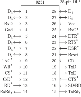
Fig. 26.6 Pin diagram of Intel 8251

Fig. 26.7 Functional pin diagram of 8251
| Vcc and Gnd: | Power supply and ground pins. 8251 uses 15V power supply. |
| D7-0: | Eight bi-directional data pins for communication with the processor. |
| RD*: | Active low input pin that is activated by the processor to read status information and receive buffer information from the 8251. |
| WR*: | Active low input pin that is activated by the processor to write to control register and to transmit buffer of the 8251. |
| CS*: | Active low input pin used for selecting the chip. |
| TxD: | It stands for Transmit Data Output pin, on which parallel data received from the processor is sent out in serial fashion. |
| TxRdy: | It is the abbreviation for Transmitter Ready. Active high output pin, which indicates to the processor that the 8251 is ready to receive a character into the transmit buffer. This output can be used to interrupt the processor. The TxRdy output is activated when the following conditions are satisfied.
It is deactivated by the 8251 when a character is written to the transmit buffer by the processor. |
| TxE: | It is the abbreviation for Transmitter Empty. Active high output pin, which indicates to the processor that the transmitter section has become completely empty—both transmit buffer and transmit shift register are now empty. It is time then to switch over from transmit mode to receive mode in the half duplex mode of operation. The TxE output can also be used to interrupt the processor. It is deactivated by the 8251 when a character is written to the transmit buffer by the processor. |
| TxC*: | It is the abbreviation for Transmitter clock. Clock input to the transmit shift register. The data is shifted out of transmit shift register in serial form on the falling edge of TxC*, for every 1, 16, or 64 clock pulses in asynchronous mode. This depends on whether the 8251 is programmed for ×1, ×16, or ×64 modes. In synchronous mode, data is shifted out for every clock pulse. |
| Clock: | The clock input is used to generate internal timing for the 8251. No external inputs or outputs are referenced to the clock input. This frequency must be at least 30 times greater than the transmitter or receiver bit rates. |
| RxD: | It is abbreviation for Receive data. Input pin on which data is received in serial fashion. This is converted to parallel form by the 8251, which is read by the processor. |
| RxC*: | It is abbreviation for Receiver clock. Clock input to the receiver Shift register. The data is shifted into the receiver shift register in serial form on the rising edge of RxC*, for every 1, 16, or 64 clock pulses in asynchronous mode. This depends on whether the 8251 is programmed for ×1, ×16, or ×64 modes. In synchronous mode, data is shifted into the receiver shift register for every clock pulse.
Intel 8251 is normally required to handle the transmission and receive operations of a single link. In such situations, the transmission and reception baud rates are required to be the same. The TxC* and RxC* pins are then connected to the same frequency source. |
| RxRdy: | It is abbreviation for Receiver Ready. Active high output pin, which indicates to the processor that the 8251 has received a character in the receiver buffer. This output can be used to interrupt the processor. The RxRdy output is activated when the following conditions are met.
|
| C/D*: | It is abbreviation for Control/Data*. It is an input pin to the 8251. When it is logic 1, the control/status register is selected and when it is logic 0, the data register—transmit buffer/receive buffer is selected. Thus, when the 8251 chip is selected, the RD*, WR*, and C/D* inputs together decide which register is going to be accessed by the processor, as indicated in the following table.
|
| Reset: | It is an active high input pin. It should remain in logic 1 state for at least six clock periods of Clk input. It is connected to ‘Reset Out’ pin of 8085. The ‘Reset Out’ pin of 8085 is activated when ‘Reset In*’ input pin of 8085 is activated. Thus, whenever the 8085 is reset, it also resets all the devices connected to ‘Reset Out’ pin of 8085. After the reset of 8251, it will be in an idle state. It will remain in idle state until a new set of command words are written to the 8251. |
| SD/BD: | It is the abbreviation for SyncDetect/Breakdetect. In the asynchronous mode of operation, this pin is used for break detection. In such a case, it is used as an active high output pin. If the RxD pin remains in logic 0 state for two character durations, the 8251 interprets it as detection of break in receive operation, in asynchronous mode. Then the BD output is activated. This output can be used to interrupt the processor. It is deactivated by the 8251 when the RxD pin receives a logic 1, or the 8251 is reset.
In the synchronous mode of operation, the same pin is used for synchronization detection. The synchronization detection can be internal or external to 8251. This is a programmable feature of 8251. It is decided by bit 6 of MI, when the 8251 is programmed for synchronous operation. If it is external synchronization detection, this pin acts as an input pin to the 8251, informing the 8251 about the detection of synchronization. The logic 1 on this pin can be removed after one RxC* cycle. If it is internal synchronization detection, this pin acts as an output pin to the 8251. This output can be used to interrupt the processor. It is deactivated by the 8251 when the processor reads the status register of 8251. Modem control pins: The use of 8251 relieves the processor from the time consuming parallel to serial conversion during transmission, and serial to parallel conversion during receive operation. However, sending information over a long distance on a single line will be expensive, unless the existing cable network, like telephone network, is used for communication. In such a case we have to use audio frequencies. So a MoDem (modulator-demodulator) working as a modulator is used for converting a logic 0 to an audio frequency of 2200Hz and a logic 1 to another audio frequency of 1200Hz, and transmitted over a carrier on the telephone network. At the receiving end, another modem, working as a demodulator, converts these frequencies back to 0s and 1s, as shown in Fig. 26.8.
Fig. 26.8 Use of modems for transmission over long distances Modems are generally called data communication equipment (DCE). The originators and terminators of data are called data terminal equipment (DTE). Thus, 8251 is a DTE. There are instances when serial communication is used even for short distance communication with a peripheral. In such cases, the peripheral is called the DCE. The interaction between DTE and DCE is handled by the following four modem control signals. |
| DTR*: | It is the abbreviation for Data Terminal Ready. This is an active low output pin. It informs the modem about the readiness of the 8251 to receive or transmit serial data. This pin is activated when the DTR bit in the CI is set to 1. The DTR bit information is inverted and sent out on DTR* pin. |
| DSR*: | It is the abbreviation for Data Set Ready. This is an active low input pin. It is used by the modem to inform the 8251 that it is ready to accept data from the 8251 for transmission. The processor can obtain the logic value on this pin by reading the MS bit of the status register of 8251. The DSR* pin information is inverted and stored in the MS bit of the status register. Thus if the MS bit of status register is 1, it means that the DSR* pin is active. |
| RTS: | It is the abbreviation for Request To Send. This is an active low output pin. It informs the modem that the 8251 has data to be transmitted. This pin is activated when the RTS bit in the CI is set to 1. The RTS bit information is inverted and sent out on RTS* pin. |
| CTS*: | It is the abbreviation for Clear to Send. This is an active low input pin. It is used by the modem to inform the 8251 that the line is clear for the 8251 to send the data. The processor has no means of reading the logic value on this pin, as the status register of 8251 does not provide this information. The information comes out on TxD pin of 8251 only if CTS* is active and the TxEn bit in CI is set to 1. When CTS* is deactivated or TxEn bit is reset to 0, the transmission is disabled after the transmission of the character in progress is completed. |

26.7 PROGRAMMING THE 8251
Prior to data transmission or reception, the 8251 must be loaded with a set of control words. This must follow a reset of 8251. The reset of 8251 can be done in the following two ways.
- By sending a logic 1 pulse on the external reset input pin of 8251. This is hardware reset.
- By setting the IR (internal reset) bit of CI to 1. This is software reset.
The control port of 8251 is used to supply to the 8251 the following types of information.
- Mode instruction;
- Synchronization character or characters;
- Command instruction.
26.7.1 MODE INSTRUCTION
Mode instruction defines the general operational characteristics of the 8251 as indicated in Fig. 26.9. Once configured, it is not expected to change during the communication process.
Thus, if 55H is the content of control port when it contains MI, it means the following:


Fig. 26.9 Control port containing MI
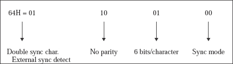
Similarly, if 64H is the content of the control port when it contains MI, it means the following:
26.7.2 COMMAND INSTRUCTION
Command instruction controls the actual operation of the 8251 as indicated in Fig. 26.10. The CI may have to be altered several times during the course of communication. For example, the transmitter might be needed to be disabled, the error bits might have to be reset, and so on.

Fig. 26.10 Control port containing CI
26.7.3 IDENTIFYING THE COMMAND IN THE CONTROL PORT
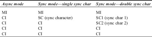
The control port contains MI, CI, or sync characters. The 8251 interprets just by the context the contents of the control port as indicated in Fig. 26.11. After a reset operation, the 8251 expects the MI to be written to the control port by the processor. This reset operation could be due to hardware reset using the reset input pin, or software reset using the IR bit of CI. The LS 2 bits of MI clearly indicate whether the 8251 is configured for synchronous or asynchronous mode.
If it is asynchronous mode, the next value written to the control port is interpreted as CI. Any subsequent value written to the control port is interpreted to be a new CI that overrides the previous CI.
If it is in synchronous mode, the MS bit of the MI decides whether the 8251 is configured for one or two sync characters. If it is configured for single sync character the next value written to the control port is interpreted as the sync character. When the control port is written the third time, it is interpreted to be CI. Any subsequent value written to the control port is interpreted to be a new CI that overrides the previous CI.
If it is configured for double sync character the next value written to the control port is interpreted as the first sync character. When the control port is written the third time, it is interpreted to be the second sync character. When the control port is written the fourth time, it is interpreted to be CI. Any subsequent value written to the control port is interpreted to be a new CI that overrides the previous CI.
Thus to enter a new MI, the 8251 has to be reset first before writing to the control port.

Fig. 26.11 Interpreting the contents of the control port
If the processor writes to the control port five times after the reset of 8251, then the interpretation of control port contents is as follows.
26.7.4 STATUS PORT OF 8251
The status information of 8251 is read by the processor when CS* = 0, C/D* = 1, and RD* =0. Both control and status ports have the same address, but control port is written by the processor, while the status port is read by the processor. The contents of the status Port Provide Status information about 8251 as indicated in Fig.26.12.
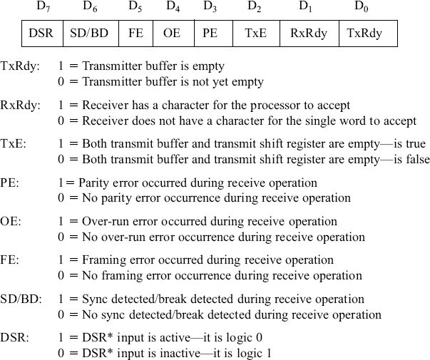
Fig. 26.12 Contents of the status port of 8251
The RxRdy pin of 8251 need not be connected toany interrupt pin of the processor. The RxRdy bit of status register can be read by the processor to find the status of the RxRdy pin. If this bit is set to 1, the processor can read from the receiver buffer of 8251. This allows status check data transfer as an alternative to interrupt driven data transfer. In a similar way, the TxE and SD/BD bits of the status register can be read by the processor to find out about the status of TxE and SD/BD pins.
The TxRdy status bit only indicates whether the transmit buffer is empy or not. The TxRdy output is activated only when the following are true.
- Transmit buffer is empty;
- The TxEn bit is set to 1 in the CI;
- CTS* input is active.
The PE, OE, and FE error bits on the status register are reset to 0 by setting the ER bit in the CI to 1. However, these error bits do not inhibit the receiver operation, even if they are set to 1.
26.8 USE OF SOD PIN OF 8085 FOR SERIAL TRANSFER
When information has to be sent by 8085 over long distances, it is economical to send it on a single line. The SOD pin canbe used for this purpose in 8085. In that case the 8085 has to convert an 8-bit parallel data to serial data and thenoutput it on SOD pin. Thus a lot of CPU time is required for such a conversion. The program to send out serial data on SOD pin is providedin the following. It is assumed that:
- Register B contains the parallel data to be transmitted in serialform on SOD pin of 8085.
- The baud rate required is 300. Hence the time for sending a bit is 1/300 s=3.33μs.
- No parity bit used.
- Two stop bits to be used.
Program
MVI A, 01000000B
       SIM ; Send a 0 (Start bit) on SOD pin.
       CALL BITTIME; subroutine for a time delay of 3.33 mSec

       MVI C, 08; C used as counter to transmit 8 data bits
AGAIN: MOV A, B
       RAR
       MOV B,A;The 3 instructions move the LS bit of B to Cy flag

       MVI A, 10000000B
       RAR; Move a bit of B which is in Cy flag to MS bit of A
       SIM
       CALL BITTIME

       DCR C
       JNZ AGAIN; Come out when 8 data bits sent out on SOD pin

       MVI A, 11000000B
       SIM
       CALL BITTIME ; Send a 1 (Stop bit) on SOD pin
       CALL BITTIME ; Send a 1 (Second Stop bit) on SOD pin
       HLT
If 8251 is available in the system, the user has to just send the parallel data into the transmit buffer of 8251. The rest would be taken care of by the 8251. This justifies the need for 8251 in a microcomputer system.
- Describe the need for a USART in a microcomputer system.
- Describe asynchronous data transmission with a neat diagram.
- Describe asynchronous data reception with a neat diagram.
- Describe synchronous data transmission with neat diagram.
- Describe the function of the pins of 8251 USART used in serial transmission.
- Describe the function of the pins of 8251 USART used in serial reception.
- Describe the function of the pins of 8251 USART used in modem control.
- Explain mode instruction of 8251 with an example.
- How is 8251 configured when the mode instruction value is 73H?
- Explain the command instruction of 8251 with an example.
- How is 8251 configured when the command instruction value is 37H?
- Explain the mechanism in 8251 for identifying the command in the control port.
- Explain the information available in the status port of 8251.
- What do we understand about the status of 8251 when the status port contains 65H?
- Write an 8085 assembly language program to receive serial data using SID pin of 8085. Assume baud rate of 2400, even parity, and 1.5 stop bits.