
18
Interrupts in 8085
![]() Data transfer schemes
Data transfer schemes
![]() Basic or simple data transfer
Basic or simple data transfer
![]() Status check data transfer
Status check data transfer
![]() Interrupt-driven data transfer
Interrupt-driven data transfer
![]() General discussion about 8085 interrupts
General discussion about 8085 interrupts
![]() EI and DI instructions
EI and DI instructions
![]() Reset_in* and Reset_out pins
Reset_in* and Reset_out pins
![]() INTR and INTA* pins
INTR and INTA* pins
![]() Action taken by 8085 when INTR pin is activated
Action taken by 8085 when INTR pin is activated
![]() Alternative action by 8085 when INTR pin is activated
Alternative action by 8085 when INTR pin is activated
![]() RST5.5 and RST6.5 pins
RST5.5 and RST6.5 pins
![]() RST7.5 pin
RST7.5 pin
![]() Trap interrupt pin
Trap interrupt pin
![]() Action taken when 8085 is interrupted due to a vector interrupt
Action taken when 8085 is interrupted due to a vector interrupt
![]() Execution of ‘DAD rp’ instruction
Execution of ‘DAD rp’ instruction
![]() SIM and RIM instructions
SIM and RIM instructions
![]() Need for masking
Need for masking
![]() SIM instruction
SIM instruction
![]() RIM instruction
RIM instruction
![]() HLT instruction
HLT instruction
![]() Programs using interrupts
Programs using interrupts
![]() Program for simulation of throwing a die
Program for simulation of throwing a die
![]() Program for simulating a stopwatch
Program for simulating a stopwatch
![]() Program to find the Square of a number using a look-up table
Program to find the Square of a number using a look-up table
![]() Program for decimal down counter
Program for decimal down counter
![]() Program for decimal down counter (alternative)
Program for decimal down counter (alternative)
![]() Program for adding 2 numbers input from keyboard
Program for adding 2 numbers input from keyboard
![]() Program for adding 4 hex digits of a 16-bit number
Program for adding 4 hex digits of a 16-bit number
![]() Questions
Questions
So far, we have discussed only 28 pins out of the 40 pins present in 8085. In this chapter, we discuss ten more pins of 8085. These are mostly related to interrupts in 8085. Also, only 242 instructions out of 246 instructions of 8085 have been discussed so far. In this chapter, the remaining four instructions, which are related to interrupts are also discussed.
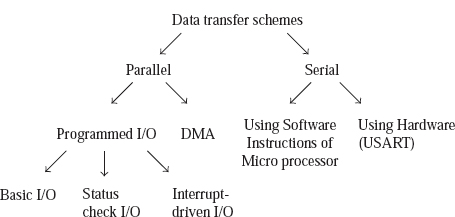
 18.1 DATA TRANSFER SCHEMES
When the 8085 is executing a program, it can get interrupted half way through the program by an I/O device. An I/O device interrupts the working of the processor, because it may want to urgently communicate with the processor. It may want to send some information to the processor, or receive some information from the processor.
A microprocessor does not directly communicate with an I/O device. It communicates with an I/O device via an I/O port. Data transfer can be in parallel or serial form. Parallel data transfer is possible using programmed I/O or Direct Memory Access (DMA). Serial data transfer and DMA data transfer are explained in later chapters. There are three different ways a microprocessor can communicate with an I/O port for parallel data transfer with programmed I/O. They are:
- Basic or simple data transfer;
- Status check data transfer;
- Interrupt-driven data transfer.
18.1.1 BASIC OR SIMPLE DATA TRANSFER
This is the simplest of the data transfer schemes. This method is useful when we have accurate know-ledge of the I/O device timing characteristics. When we know that the device is ready for data transfer, we execute IN or OUT instruction, depending on the required direction of data transfer. This is the case when the I/O port is connected in the system as an I/O-mapped I/O port. If the port is connected as a memory-mapped I/O port, ‘MOV M, A’, ‘MOV A, M’, or any other memory reference instruction is used depending on the direction of data transfer.
As an example, let us say we have a hypothetical multiplier chip. Registers R0 and R1 are used to load the two 8-bit numbers to be multiplied. The 16-bit product will be available in R2H and R2L when the multiplication is over. Address pins A1 and A0 select a register as shown in the following.
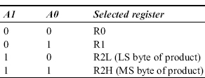
Let us say the chip is connected as I/O-mapped I/O, as shown in Fig. 18.1. As per the chip select circuit, the address for R0, R1, R2L, and R2H is 40H, 41H, 42H, and 43H, respectively. Let us say the data sheet for the multiplier specifies a maximum of 50 μs for completing the multiplication.

Fig. 18.1 Simple I/O data transfer
With this set up, the following program segment performs multiplication of 05H and 08H, and the result will be stored in the BC register pair.
MVI A, 05H
OUT 40H        ;Load R0 with 05H
MVI A, 08H
OUT 41H        ;Load R1 with 08H
CALL DELAY     ;Generate a delay of 50 micro seconds
;The subroutine is not shown for simplicity
IN 42H
MOV C, A       ;Store LS byte of product in C register
IN 43H
MOV B, A       ;Store MS byte of product in B register
In the previous example, even if the multiplication is over in 20 ms, we are required to wait for 50 μs, as per the data sheet. The advantage of simple I/O is its simplicity, but its disadvantage is that it is not very efficient. We come across a number of examples later in the text for this type of data transfer. The flowchart for simple I/O is illustrated in Fig. 18.2.
18.1.2 STATUS CHECK DATA TRANSFER
This is more complex than simple data transfer. This method is used when we do not have accurate knowledge of the I/O device timing characteristics. The processor should get status information about the readiness of the I/O device for data transfer. Generally, the processor will be in a loop checking for the readiness of the device. The moment the device is ready, it comes out of the loop, and executes IN or OUT instruction depending on the requirement. In this case, the processor has simply wasted its time in a loop till the device got ready.
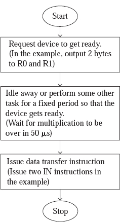
Fig. 18.2 Flowchart for simple I/O
As an example, let us once again consider the hypothetical multiplier chip. Let the chip be provided with command and status registers also. Let us say when the MS bit of the command register is set to 1, it is a command to start the multiplication of the two numbers in R0 and R1. Let us say the LS bit of the status register is set to 1 when the product is available in R2H and R2L.
Address pins A2, A1, and A0 select a register as shown in the following.

Let us say the chip is connected as I/O-mapped I/O, as shown in Fig. 18.3. As per the chip select circuit, the address for R0, R1, R2L, R2H, command register and status register is 40H, 41H, 42H, 43H, 44H, and 45H, respectively.
In this case, the microprocessor sends the two bytes to be multiplied to the registers R0 and R1. Then a command is issued to start the multiplication process. This is done by setting the MS bit of the command register. Then the status register is continuously monitored for the completion of the multiplication operation. This is done by checking the LS bit of status register. When the LS bit of status register becomes 1, the microprocessor reads the result.
With this set up, the following program segment performs multiplication of 05H and 08H, and the result will be stored in the BC register pair.

Fig. 18.3 Status check data transfer
MVI A, 05H
            OUT 40H        ;Load R0 with 05H
            MVI A, 08H
            OUT 41H        ;Load R1 with 08H
            MVI A, 10000000B
            OUT 44H        ;Issue Start multiplication command
WAIT: IN 45H
            RRC
            JNC WAIT       ;Be in wait loop till LS bit of Status
                           ;register becomes 1
            IN 42H
            MOV C, A       ;Store LS byte of product in C register
            IN 43H
            MOV B, A       ;Store MS byte of product in B register
In status check I/O, as soon as the device is ready, the data transfer is performed. Status check I/O is more efficient than simple I/O, but is more complex. This method of data transfer is also known as handshake data transfer.
We come across a number of examples later in the text for this type of data transfer. The flowchart for status check I/O is illustrated in Fig. 18.4.

Fig. 18.4 Flowchart for status check I/O
18.1.3 INTERRUPT-DRIVEN DATA TRANSFER
This method is used when we do not have accurate knowledge of the I/O device timing characteristics, except that it takes quite a long time for the device to get ready. If we resort to status check data transfer, the processor will have to waste a long time in the loop for the device to get ready. To avoid this problem, interrupt-driven data transfer can be used. In this case, the processor will go ahead with its required work, and whenever the device gets ready for data transfer, the corresponding I/O port will send a interrupt request signal to the processor. The interrupt request may arrive even half way through an instruction execution. Then the processor will complete the instruction. After this, the processor will perform data transfer with the I/O device using IN or OUT instruction. Then it resumes the execution of the interrupted program. Flowchart for interrupt-driven data transfer is provided in Fig. 18.5a.
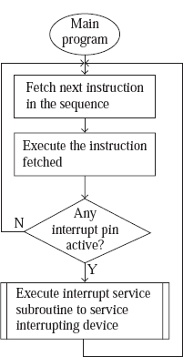
Fig. 18.5a Flowchart for interrupt-driven data transfer
This method is obviously the most complex of the three types of data transfer. But the advantage now is that the processor is not wasting its time in a loop checking for the readiness of the I/O device.
For example, if the 8085 wants to read from a keyboard, one way is to continuously scan the keyboard looking for a pressed key. This is the status check method. It may so happen that once in a second or so, it finds that a key is pressed. The 8085 is in a loop for this amount of time just waiting for a key depression. In this time, the 8085 could have executed about 500,000 instructions, assuming an average execution time of 2 μs per instruction! In interrupt-driven data transfer, the 8085 would execute about 500,000 useful instructions, by which time the user presses a key on the keyboard. This causes an interrupt signal to be sent to the 8085 by the I/O port. Then the 8085 reads from the port attached to the keyboard, after which it goes ahead with the program.
In the remaining portion of this chapter, we mainly discuss the interrupt pins of 8085, interrupt-related instructions, and some programs that use interrupts. These programs clearly describe the interrupt-driven data transfer.
18.2 GENERAL DISCUSSION ABOUT 8085 INTERRUPTS
Interrupt pins of 8085 are used by I/O devices to initiate transfer of data to or from 8085, without wasting much of the CPU time. As seen previously, this is very useful, when the timing characteristics of the I/O device is not well known, and it takes a long time for the device to get ready for data transfer. There are five interrupt pins on 8085, as shown in Fig. 18.5b. They are input pins of 8085. They are TRAP, RST7.5, RST6.5, RST5.5, and INTR.
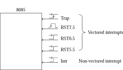
Fig. 18.5b Interrupt pins of 8085
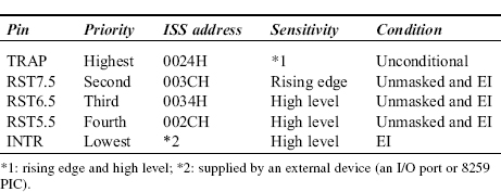
Note that RST7, RST6, and RST5 are instructions of 8085, whereas RST7.5, RST6.5, and RST5.5 are interrupt pins of 8085. An interrupt pin can be activated by an I/O port even half way through an instruction, without having any relation to a clock signal. Thus the interrupts are asynchronous in nature. The 8085 checks all these interrupt pins at about the end of every instruction. Specifically, they are checked in the penultimate clock cycle of the last machine cycle of an instruction. However, the interrupt pins are not checked at the end of an instruction, if the instruction belongs to the branch group, JMP, CALL, RET, etc. In such cases, the interrupt requests are sensed after a lapse of about 15 clock cycles. At this point, if several interrupts are active simultaneously, the 8085 services them as per the priority shown in the table that follows.
When an I/O port activates one of these pins, the 8085 gets interrupted if each of the following conditions are satisfied.
- The interrupt system is enabled by setting the interrupt enable (IE) flip-flop of 8085. This condition is not applicable to TRAP. The method of setting the interrupt enable flag is discussed later.
- The interrupt pin has not been masked. This condition is not applicable to TRAP and INTR. The method of masking or unmasking an interrupt pin is discussed later.
- Higher priority interrupts are not active at the same time.
The following is the broad action taken by the 8085 when it gets interrupted. Finer details are given later in the chapter.
- It completes the execution of the current instruction.
- Stores on the stack top the address of the next instruction, called Return address, which is present in the program counter.
- Program branches to a subroutine, whose execution satisfies the I/O device that interrupted the 8085. This subroutine is thus named as an interrupt service subroutine or ISS. Details of ISS address are provided later in the chapter.
- Normally an ISS consists of three portions. The first portion is used for saving on the stack all the register values of 8085 that are going to be affected by the execution of the ISS. Thus, it uses a number of PUSH instructions. The next portion will have instructions to achieve the actual purpose of the ISS. If the purpose is data transfer, we will have IN or OUT instruction in this part. However, if the I/O port is connected as memory-mapped I/O, a memory reference instruction will be used for data transfer with the I/O port. The last part is used for restoring the original values to various registers that were affected by the second part of ISS. As such, it contains a number of POP instructions. The ISS then ends with EI and RET instructions. The purpose of EI instruction will be discussed later. The typical layout of an ISS is provided in Fig. 18.6.
- After completely executing the ISS, the control returns to the program that was interrupted. This is done by popping the top of stack information to the PC, using RET instruction at the end of ISS.

Fig. 18.6 Typical layout of an ISS
18.3 EI AND DI INSTRUCTIONS
In the previous section, a broad outline was provided regarding the action to be taken by the 8085 when an I/O port activated an interrupt pin. The finer details are discussed in the rest of the chapter.
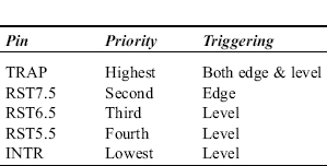
The 8085 can be thought of as having five internal interrupt signals that correspond to the five external interrupt pins. Only when the internal interrupt signal is activated, the 8085 gets interrupted, provided higher priority internal interrupt signals are not active at the same time. The 8085 checks all these internal interrupt signals in the penultimate clock cycle of the last machine cycle of an instruction.
There is a flip-flop in 8085 called IE flip-flop. Here IE stands for Interrupt Enable. Whenever this flip-flop is reset to the 0 state, 8085 interrupt system is disabled. That is, even if an external interrupt pin is activated, the corresponding internal interrupt signal is not activated. This can be seen from Fig. 18.7, which provides the internal architecture of 8085 interrupt structure. From this figure it can also be noticed that this flip-flop state has nothing to do with the internal interrupt signal corresponding to TRAP. TRAP is a non-maskable interrupt. It means whenever the external TRAP pin is activated, the corresponding internal interrupt signal is always activated. Further, TRAP being the highest priority interrupt, it always interrupts the 8085.
The IE flip-flop is reset to the 0 state by the following three conditions as shown in Fig. 18.7.
- Execution of DI instruction;
- Recognition of an interrupt request;
- Resetting of 8085.
The DI instruction stands for ‘disable interrupts’. It is an 1-byte instruction. When this instruction is executed, the IE flip-flop is reset. This disables the 8085 interrupt system except for the TRAP pin.
When the 8085 recognizes an interrupt, it branches to an ISS. By recognition we mean that, an internal interrupt signal is activated, and higher priority internal interrupt signals are not active. In the ISS, the 8085 would not like to be interrupted again. That is the reason, as to why the 8085 will place itself in DI state, when it recognizes an interrupt. However, TRAP can still interrupt an ISS. Thus, when the control is transferred to an ISS, interrupt system is disabled automatically. Accordingly, there is no need for the programmer to write a DI instruction at the beginning of an ISS. Whether the programmer writes a DI instruction at the beginning of an ISS or not, interrupt system remains disabled, except for TRAP.
18.3.1 RESET_IN* AND RESET_OUT PINS
Intel 8085 has a RESET_IN* pin. This is an active low input pin. The 8085 is reset by placing a logic 0 on this pin for atleast 0.5μs, after power is supplied to Vcc pin of 8085. However, in practice the RESET_IN* is placed in logic 0 state for atleast a few milliseconds. A typical reset circuit, used in ALS 8085 kit, is shown in Fig. 18.8.
The moment power supply is switched on, Vcc pin gets +5 V power. However, the RESET_IN* pin remains in the logic 0 state for a time dependent on the RC time constant. In the circuit in Fig. 18.8, the RC time constant is about 50ms. Thus, the RESET_IN* pin will be in logic 0 for a time longer than the minimum required 0.5μs.
When the system is already powered and running, sometimes we need to reset the 8085. There is no need to switch off, and then switch on, to reset the 8085. There is a manual reset switch as shown in Fig. 18.8. When we momentarily press and release it, the RESET_IN* pin goes to logic 0, and then comes back to logic 1 state after a time dependent on the RC constant. In this case, if the RESET_IN* pin is kept at logic 0 for atleast three clock cycles (1μs) the 8085 will be reset.
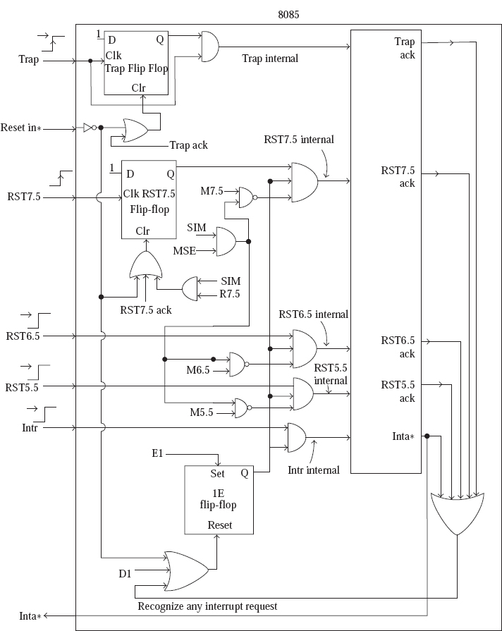
Fig. 18.7 Architecture of 8085 interrupt structure
Fig. 18.8 Reset circuit for 8085
Some of the important actions performed by the 8085 when it is reset are as follows.
- PC contents becomes 0000H.
- IR contents becomes 00H.
- All interrupts, except TRAP, are disabled by resetting IE flip-flop.
- RST7.5, RST6.5, and RST5.5 interrupts are masked (masking is explained later in the chapter).
- SOD pin output becomes (discussed later).
- RST7.5 flip-flop will be reset to 0 (discussed later).
If the RESET_IN* signal is at logic 0, the 8085 sends out a logic 1 on the RESET_OUT pin at the beginning of the next clock cycle. This is an active high signal. RESET_OUT goes to the logic 0 state only in the next clock cycle after RESET_IN* goes to logic 1 state. This RESET_OUT signal is used to reset other chips in the microcomputer system, such as 8255 PPI, 8251 USART, etc. The timing relationship between RESET_IN* and RESET_OUT is shown in Fig. 18.9.

Fig. 18.9 Timing relationship between RESET_IN* and RESET_OUT
Earlier, we have discussed the method of resetting to 0, the IE flip-flop. Now let us discuss the method of setting to 1 the IE flip-flop. It is achieved by the execution of the EI instruction. The EI instruction stands for ‘enable interrupts’. It is an 1-byte instruction. When this instruction is executed, the IE flip-flop is set to 1. This enables the 8085 interrupt system. But the interrupts will be enabled only after the next instruction after EI is executed. The reason for this is as follows.
It was stated earlier that when the 8085 branches to an ISS, the interrupt system is disabled automatically. Thus, before we come out of the ISS, it is necessary to again enable the interrupt system using EI instruction. Otherwise, when the control is back with the interrupted program, it cannot be interrupted again, except by TRAP. But immediately after EI, the interrupt system should not get enabled. If it gets enabled, there is the danger of branching to another ISS before the RET instruction in the current ISS is executed. To overcome this problem, the interrupt system gets enabled only after one instruction is executed subsequent to the execution of the EI instruction. Thus, if we end an ISS with EI followed by RET, the interrupt system is enabled only when the control is back with the interrupted program.
18.4 INTR AND INTA* PINS
INTR is an active high input pin. This is having the lowest priority. It can interrupt the 8085 only if the 8085 is not required to service any other interrupt at the same time. It is a level-sensitive input. The line should remain high till the 8085 checks the internal interrupt signal corresponding to INTR at about the end of an instruction. The INTR internal interrupt signal is activated only when INTR pin is in logic 1 state and IE flip-flop is in logic 1 state, as can be seen from Fig. 18.7. The 8085 gets interrupted because of INTR pin, only if the following conditions are met.
- INTR internal interrupt signal is active.
- Higher priority internal interrupt signals are not active at the same time.
If these conditions are not met, even though INTR pin is activated, the 8085 does not get interrupted. In such a case, the INTR line should remain high till the above conditions are met in order to interrupt the 8085.
We always start with a reset of the 8085, because of the switching on of the microcomputer system. Thus, all interrupts except TRAP are disabled to start with. So, if we want INTR pin activation to interrupt the 8085, it is necessary that we have EI instruction in our program. The interrupt system will then be enabled after executing the next instruction after EI. It is important to note that without EI instruction in the main program, the main program will never be interrupted by any of the 8085 interrupts, except TRAP.
INTR is a non-vectored interrupt in 8085. By this we mean that the 8085 does not know by itself the starting address of the ISS. It has to be provided to the 8085 by an external I/O port, or by an interrupt controller like Intel 8259. The action taken by the 8085 when INTR pin is activated is detailed in the following.
18.4.1 ACTION TAKEN BY 8085 WHEN INTR PIN IS ACTIVATED
It is assumed that interrupt system is enabled using EI instruction, and higher priority internal interrupt signals are not active.
- In the penultimate clock cycle of the last machine cycle of every instruction, the 8085 senses all the internal interrupt signals.
- If INTR internal signal is at logic 1, the 8085 enters an interrupt acknowledge (INA) machine cycle.
- The interrupt from the I/O port is acknowledged by the 8085 by activating INTA* pin in the T2 state of the INA machine cycle. INTA* is an active low pin. In response to INTA*, the interrupting port should send code for CALL instruction to IR register of 8085 on AD7-0 pins. Intel 8259 interrupt controller is capable of sending such a CALL instruction to 8085. Intel 8259 is discussed in a later chapter. Note that the CALL instruction does not come from memory in this case. So this M1 machine cycle is not an OF machine cycle from memory. Also, it is not an IOR machine cycle, because INTA* is activated, and not RD*. In this INA machine cycle, IO/M*, S1, and S0 will all be in 1 state. This INA machine cycle is shown in Fig. 18.10. INTA* signal becomes a 1 after the 8085 receives the code for CALL during this INA machine cycle. This INA machine cycle that fetches the code for CALL and decodes it, uses six T states.

- In M2 machine cycle, which is also an INA machine cycle, LS byte of ISS address is transferred to the Z register of 8085 by the 8259. This will be in response to activation of INTA* during T2 of this INA machine cycle. This machine cycle uses only three T states, as the 8085 does not have to decode this information.
- In M3 machine cycle, which is also an INA machine cycle, MS byte of ISS address is transferred to the W register of 8085 by the 8259. This will be in response to activation of INTA* during T2 of this INA machine cycle. This machine cycle also uses only three T states, as the 8085 does not have to decode this information. Now the 8085 has received the complete ISS address. After this, save on the stack top the return address available in PC, before branching to the ISS.
- In M4, which is a MW machine cycle, MS byte of the PC is pushed onto the stack. This takes three T states.
- In M5, which is also a MW machine cycle, LS byte of PC is pushed onto the stack. At this point, the address specified in the CALL instruction, which is present in the WZ register pair, is moved to the PC. All this takes three T states. This results in the starting of the ISS execution.
It can be noticed from these points that, after completion of the instruction during which the 8085 got interrupted, it takes 6 + 3 + 3 + 3 + 3 = 18 T states before the 8085 transfers control to the ISS.
Incidentally, digressing a bit, it may be appropriate to describe the fetching and execution of a 3-byte CALL instruction stored in memory. This also needs 18 T states, but the machine cycles involved are: six T-state OF, followed by two MR machine cycles each of three T states, and two MW machine cycles each of three T states.
18.4.2 ALTERNATIVE ACTION BY 8085 WHEN INTR PIN IS ACTIVATED
In response to activation of INTA*, instead of CALL instruction, an RST instruction can be transferred to the IR register of 8085 by an I/O port. The RST instruction is only an 1-byte instruction, and so there will be saving of time in receiving the instruction. The action taken by 8085 during this alternative will be as follows.
It is assumed that the interrupt system is enabled using EI instruction, and higher priority internal interrupt signals are not active.
- In the penultimate clock cycle of the last machine cycle of every instruction, the 8085 senses all the internal interrupt signals.
- If INTR internal signal is at logic 1, the 8085 enters an INA machine cycle.
- The interrupt from the I/O port is acknowledged by the 8085 by activating INTA* pin in the T2 state of INA machine cycle. In response to INTA*, an I/O port should send code for an RSTn (n = 0 to 7) instruction to IR register of 8085 on AD7-0 pins. An I/O port chip like Intel 8255 is capable of sending such an RSTn instruction to 8085. Intel 8255 is discussed in a later chapter. Note that the RSTn instruction does not come from the memory in this case. So this M1 machine cycle is not an OF machine cycle from memory. Also, it is not an IOR machine cycle, because INTA* is activated, and not RD*. In this INA machine cycle, IO/M*, S1, and S0 will all be in 1 state. This INA machine cycle has already been shown in Fig. 18.10. INTA* signal becomes a 1 after the 8085 receives the code for RSTn during this INA machine cycle. This INA machine cycle that fetches the code for RSTn and decodes it, uses six T states. Now the 8085 knows that it has to transfer control to the ISS at location n * 8. For example, if the instruction received was RST6, the control should be transferred to the ISS at 6 * 8 = 0030H. This address will be internally stored in the WZ register pair by the control unit of 8085. Now it is required to first of all save on the stack top the return address available in the PC, before branching to the ISS.
- In M2, which is a MW machine cycle, MS byte of PC is pushed onto the stack. This takes three T states.
- In M3, which is a MW machine cycle, LS byte of PC is pushed onto the stack. At this point, the ISS address, which is present in the WZ register pair, is moved to the PC. This takes three T states. This results in the starting of the ISS execution.
It can be noticed from these points that, after completion of the instruction during which the 8085 got interrupted, it takes 6 + 3 + 3 = 12 T states before the 8085 transfers control to the ISS.
Generally at location 6 * 8 we will not have the ISS. For example, in the ALS kit there is JMP FFA8H instruction in the 3 bytes starting at 6 * 8 = 0030H. FFA8H is a system RAM location in ALS kit. The system RAM area is used by the kit for storing system data. As such, the ISS cannot start at location FFA8H also. In this system RAM area, 3 bytes starting from FFA8H are reserved for the user to store a jump instruction, say C900H. In such a case, the ISS for INTR when RST6 is received in response to INTA*, starts at location C900H. This is illustrated in Fig. 18.11.
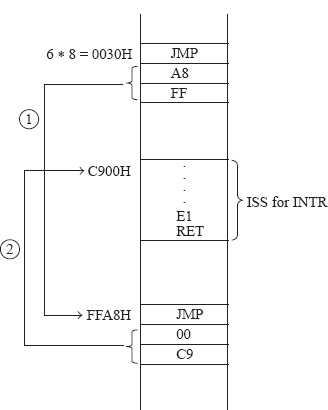
Fig. 18.11 Jumping to ISS when RST6 is received by 8085
Incidentally, digressing a bit, it may be appropriate to describe the fetching and execution of the single-byte RSTn instruction stored in the memory. This also needs 12 T states, but the machine cycles involved are: six T-state OF, followed by two MW machine cycles each of three T states.
18.5 RST5.5 AND RST6.5 PINS
Both RST5.5 and RST6.5 pins are level-sensitive inputs. RST6.5 has a higher priority than RST5.5. RST5.5 in turn has higher priority than INTR. The function of RST5.5 and RST6.5 are very similar. These pins should remain high till the 8085 checks all the internal interrupt signals at about the end of an instruction. As can be easily seen from Fig. 18.7, the RST5.5 and RST6.5 internal interrupt signals are activated only when
- These external interrupt pins are in logic 1 state;
- IE flip-flop is in logic 1 state;
- These interrupts are not masked by the SIM instruction.
The 8085 gets interrupted because of RST5.5 or RST6.5 pin, only if the following conditions are met.
- RST5.5 or RST6.5 internal interrupt signal is active;
- Higher priority internal interrupt signals are not active.
If these conditions are not met, even though RST5.5 or RST6.5 pins are activated, the 8085 does not get interrupted. In such a case, these pins should remain high till these conditions are met in order to interrupt the 8085.
As we always start with a reset of the 8085, because of the switching on of the microcomputer system, all interrupts except TRAP are disabled to start with. So, if we want these pins to interrupt the 8085, it is necessary that we have EI instruction in our program. The interrupt system will then be enabled after executing the next instruction after EI.
RST5.5 and RST6.5 are vectored interrupts in 8085. By this we mean that the 8085 knows by itself the starting address of the ISS. It is 5.5 * 8 = 002CH in the case of RST5.5, and 6.5 * 8 = 0034H in the case of RST6.5. The action taken by 8085 when RST5.5 or RST6.5 is activated, is discussed a little later.
Generally at locations 5.5 * 8 and 6.5 * 8 we will not have the ISS. For example, in the ALS kit there is JMP 05C3H instruction in the 3 bytes starting at 5.5 * 8 = 0024H. 05C3H is an EPROM location in ALS kit. The EPROM contains the monitor program. At 05C3H in the EPROM there is ISS for RST5.5. In the ALS kit, whenever the user presses a key on the keyboard (except RESET key and VECT INTR key), the RST5.5 pin of 8085 is activated. Thus, in ALS kit the RST5.5 interrupt pin is used by the keyboard to interrupt the 8085. Similarly, at location 6.5 * 8 we will not have the ISS. For example, in the ALS kit there is JMP FFABH instruction in the 3 bytes starting at 6.5 * 8 = 0034H. FFABH is a system RAM location in ALS kit. The system RAM area is used by the kit for storing system data. As such, the ISS cannot start at location FFABH also. In this system RAM area, 3 bytes starting from FFABH are reserved for the user to store a jump instruction, say CC00H. In such a case, the ISS for RST6.5 starts at location CC00H.
18.6 RST7.5 PIN
RST7.5 pin is an edge-sensitive input. This is used by peripherals that send a pulse, rather than a sustained high level, for interrupting the processor. Internal to 8085 there is a flip-flop connected to RST7.5 interrupt pin. This flip-flop is set to 1, when a positive-going edge occurs on RST7.5 input. This can be visualized from Fig. 18.7. The waveform for RST7.5 pin and Q output of RST7.5 flip-flop is shown in Fig. 18.12.
RST7.5 internal interrupt signal has a higher priority than the internal interrupt signals of RST6.5, RST5.5, and INTR. As can be seen from Fig. 18.7, the RST7.5 internal interrupt signal is activated only when
- Q output of the RST7.5 flip-flop is at logic 1;
- IE flip-flop is in logic 1 state;
- RST7.5 interrupt is not masked by SIM instruction.
The 8085 gets interrupted because of RST7.5 pin, only if the following conditions are met.
- RST7.5 internal interrupt signal is active;
- TRAP internal interrupt signal is not active.
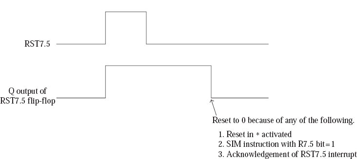
Fig. 18.12 Waveform of RST7.5 pin and RST7.5 flip-flop
If these conditions are not met, even though a rising edge occurs on RST7.5 pin, the 8085 does not get interrupted. As we always start with a reset of the 8085, because of the switching on of the microcomputer system, all interrupts except TRAP are disabled to start with. So, if we want the RST7.5 pin to interrupt the 8085, it is necessary that we have EI instruction in our program. The interrupt system will then be enabled after executing the next instruction after EI.
RST7.5 is a vectored interrupt in 8085. By this we mean that the 8085 knows by itself the starting address of the ISS. It is 7.5 * 8 = 003CH. The action taken by 8085 when RST7.5 is activated is discussed a little later.
Generally at location 7.5 * 8 we will not have the ISS. For example, in the ALS kit there is JMP FFB1H instruction in the 3 bytes starting at 7.5 * 8 = 003CH. FFB1H is a system RAM location in ALS kit. As such, the ISS cannot start at location FFB1H also. In this system RAM area, 3 bytes starting from FFB1H are reserved for the user to store a jump instruction, say CD00H. In such a case, the ISS for RST7.5 starts at location CD00H.
There is no pin of 8085 that can be used to reset the RST7.5 flip-flop. So, RST7.5 flip-flop has to be reset by software. The SIM instruction, to be discussed a little later, can be used to reset the RST7.5 flip-flop. Also, the moment when the 8085 recognizes RST7.5 interrupt request and branches to ISS, the RST7.5 flip-flop is automatically reset to 0.
18.7 TRAP INTERRUPT PIN
Trap is a non-maskable interrupt. This implies that whenever this pin is activated, the 8085 will always get interrupted, even if the 8085 is in DI state. Trap input is both edge- and level-sensitive. Thus the Trap line must make a transition from 0 to 1, and must remain in 1 state till the end of the execution of an instruction in order to interrupt the 8085. Figure 18.13 shows the conditions for which Trap input can cause interrupt of 8085. In this figure t0 indicates the time at which an instruction execution starts and t1 indicates the time at which it ends.
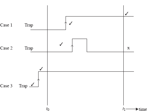
Fig. 18.13 Condition for trap to interrupt the 8085
In Fig. 18.13, only in case 1, the Trap input interrupts the 8085 at time t1. This is because both the edge and level conditions are satisfied. In case 2, the level condition is not satisfied at time t1. In case 3, the edge condition is not satisfied at time t1. However in case 3, 8085 is interrupted because of interrupt at t0 itself.
At this point it is appropriate to note that an interrupt input is deactivated by an I/O port only after the port is serviced by the 8085. The port needs to perform data transfer with 8085 in the ISS in order that the port is satisfied. This generally happens at about the middle of an ISS. This is in view of the instructions to save the registers in the beginning of the ISS, and instructions to restore registers at the end of the ISS. Thus, an interrupt pin is deactivated by an I/O port only in the middle of the ISS.
Now, it should be clear as to why the Trap input should be both edge- and level-sensitive. If it were to be just edge-sensitive, it would have been susceptible to noise. If it were to be only level-sensitive the problem would be as follows. The Trap pin would still be in the logic 1 state till at about the middle of the ISS, as explained previously. So surely at the end of the first instruction in the ISS, the Trap pin will still be in logic 1 state causing the 8085 to again get interrupted because of the Trap. To solve this problem, Trap is designed to be both edge- and level-sensitive.
Internal to 8085 there is a flip-flop connected to the Trap interrupt pin. As can be seen from Fig. 18.7, the Trap internal interrupt signal is activated whenever a 0 to 1 transition occurs on Trap pin, and the Trap pin remains in the 1 state till the end of an instruction. Trap internal interrupt signal has a higher priority than all the other internal interrupt signals of 8085. So, whenever the Trap internal interrupt signal is activated, the 8085 gets interrupted even if 8085 is in DI state.
The moment when the 8085 recognizes Trap interrupt request and branches to ISS, the Trap flipflop is automatically reset to 0. It is also reset by activation of reset input of 8085, as can be seen from Fig. 18.7. Thus, even if the external Trap signal remains at logic 1, it cannot further interrupt the 8085 in the ISS for Trap. To again interrupt the 8085, the external Trap signal should be brought to logic 0, then it must go to logic 1, and remain at logic 1 till the end of the instruction to interrupt the 8085.
Trap is a vectored-interrupt in 8085. The 8085 knows by itself the starting address of the ISS as 4.5 * 8 = 0024H. Thus, Trap pin could have been named equivalently as RST4.5 pin. However, Intel prefers to refer to it as Trap. This is probably because, in computer terminology, Trap is a nonmaskable interrupt, whereas an interrupt is a maskable one. The action taken by 8085 when Trap is activated is discussed a little later.
Generally at location 4.5 * 8 we will not have the ISS. For example, in the ALS kit there is JMP 0182H instruction in the 3 bytes starting at 4.5 * 8 = 0024H.
In the ALS kit, memory location 0182H is in the EPROM. The EPROM contains the monitor program. At 0182H in the EPROM there is ISS for trap. In the ALS kit, the trap interrupt is used for single-stepping through the program, for debugging purposes.
18.7.1 ACTION TAKEN WHEN 8085 IS INTERRUPTED DUE TO A VECTOR INTERRUPT
We already know that the vector interrupts in 8085 are trap, RST7.5, RST6.5, and RST5.5. Let us say a vector interrupt pin is active. As an example, let us assume that RST6.5 interrupt pin is active. As was discussed earlier, RST6.5 interrupt pin will interrupt the 8085 only when the following conditions are satisfied.
- RST6.5 interrupt pin is activated;
- The 8085 interrupt system is enabled;
- RST6.5 has not been masked, using SIM instruction;
- Higher priority internal interrupt signals, trap and RST7.5 are not active.
Similarly, the condition for the other vector interrupts to cause an interrupt to the 8085 has already been discussed. However, the action taken by the 8085 when it gets interrupted because of any vector interrupt, is almost the same. Hence, only the action taken when 8085 is interrupted because of RST6.5 interrupt pin is explained as follows.
The 8085 recognizes the RST6.5 interrupt at about the end of the execution of an instruction. At the end of this instruction, the 8085 enters a (BI) machine cycle. In this BI machine cycle, we can imagine that the IR register is loaded with the code for ‘RST6.5’ instruction. However, there is no such instruction in reality. As such, we can as well imagine that the IR register is loaded with code for CALL instruction, and the WZ register pair is loaded with 6.5 * 8 = 0034H. This is because, RST6.5 is equivalent to CALL 0034H. This happens the moment when the 8085 recognizes RST6.5 interrupt. The 8085 spends three clock cycles for decoding it. Decoding is purely an internal operation for 8085. During this time, there is no activity on address, data, or control bus. Hence the name ‘bus idle’ for this machine cycle is justified. This BI machine cycle, which is the first machine cycle M1, needs only three clock cycles (compared with the six clock cycles needed for the first INA machine cycle when INTR causes interrupt to 8085). This is because, the opcode does not have to come from memory or I/O ports. There cannot be any wait states in the BI machine cycle. This is because neither memory, nor I/O port is communicating with 8085 in the BI machine cycle.
The 8085 then stores the contents of the PC, which is the return address, on the stack. M2, which is a MW machine cycle, is used for storing PCH (high byte of PC) on the stack top. It takes three clock cycles.
Similarly, M3, which is also a MW machine cycle, is used for storing PCL (low byte of PC) on the stack top. Then the PC is loaded with 0034H from the WZ register pair. This takes a total of another three clock cycles.
Generally, at location 0034H we will not have the ISS. For example, in the ALS kit there is JMP FFABH instruction in the 3 bytes starting at 0034H. FFABH is a system RAM location in ALS kit. The system RAM area is used by the kit for storing system data. As such, the ISS cannot start at location FFABH also. In this system RAM area, 3 bytes starting from FFABH are reserved for the user to store a jump instruction, say CC00H. In such a case, the ISS for RST6.5 starts at location CC00H.
Thus, when the 8085 gets interrupted because of a vector interrupt, there will be a BI machine cycle followed by two MW machine cycles. The only other occasion when the 8085 enters a BI machine cycle is during the execution of ‘DAD rp’ instruction.
18.8 EXECUTION OF ‘DAD rp’ INSTRUCTION
Let us digress a bit at this point to discuss about the execution of the ‘DAD rp’ instruction. As an example, let us study the execution of the DAD B instruction. If content of BC is 5678H, and content of HL is 12A7H, execution of DAD B should result in HL having 691FH, as shown in the following.
- (BC) = 56 78H
- (HL) = 12 A7H
- _____________
- (HL) = 69 1FH
In the first machine cycle M1, the opcode for DAD B instruction is fetched from the memory into the IR register of 8085. This is then decoded by the 8085 to interpret it as the opcode for DAD B instruction. This OF machine cycle takes a total of 3 + 1 = 4 clock cycles. Now it is required to add the contents of HL and BC register pairs. Thus the data needed for this instruction execution is available within the 8085. It is similar to ADD B instruction, where the data needed for instruction execution is available within 8085. Generally in such cases the execution portion takes only a fraction of a clock cycle. But in the case of DAD B, as the required operation is addition of 16-bit numbers, it needs much larger time. This is because, in 8085 we have only an 8-bit ALU, with accumulator and temp registers providing the two inputs to the ALU.
In the second machine cycle M2, the following actions take place.
- Accumulator is temporarily stored in the W register;
- L register contents are moved to the accumulator;
- C register contents are moved to the temp register;
- Addition is performed, and ALU output is moved to the L register.
This machine cycle uses up three clock cycles. It is a BI machine cycle because:
- No address is sent out by 8085;
- No data is sent out or received from outside;
- No external control signals are generated by 8085.
In the third machine cycle M3, the following actions take place.
- H register contents are moved to the accumulator;
- B register contents are moved to the temp register;
- Addition with Cy is performed, and the result stored is in H;
- Accumulator gets the original value from the W register.
This machine cycle uses up three clock cycles. This is also a BI machine cycle because:
- No address is sent out by 8085;
- No data is sent out or received from outside;
- No external control signals are generated by 8085.
Thus, the DAD B instruction needs a total of ten clock cycles. It consists of OF machine cycle (four clock cycles), followed by two BI machine cycles (each of three clock cycles).
18.9 SIM AND RIM INSTRUCTIONS
It was noted earlier that RST7.5, RST6.5, and RST5.5 interrupt pins can be masked or unmasked. But then what is the need for masking?
18.9.1 NEED FOR MASKING
Let us say, the 8085 has been interrupted because of RST6.5 pin and has branched to the ISS for RST6.5. Then, even without DI instruction at the beginning of this ISS, all the interrupts except TRAP are disabled. So, even if RST7.5 pin is activated in the middle of the execution of RST6.5 ISS, the 8085 will not get interrupted because of RST7.5. Actually RST7.5 is a higher priority interrupt, but now it cannot interrupt the lower priority ISS of RST6.5! We can hope to solve this problem by specifically having EI instruction at the beginning of the ISS for RST6.5. Now RST7.5 can definitely interrupt the RST6.5 ISS, but the problem is that even RST5.5 can interrupt the RST6.5 ISS!
This problem can be solved using the concept of masking of interrupts. It provides the ability to selectively disable the interrupts. An interrupt pin that is masked cannot interrupt, even if the interrupt pin is activated and interrupts are in general enabled using EI instruction. Similarly, an interrupt pin that is unmasked can interrupt, when the interrupt pin is activated and interrupts are in general enabled using EI instruction.
Thus, all that is needed to prevent RST5.5 from interrupting RST6.5 ISS, while allowing RST7.5 to interrupt the RST6.5 ISS is:
- Enable the interrupt system using EI instruction;
- Mask RST5.5 so that it cannot interrupt the ISS;
- Unmask RST7.5 so that it can interrupt the ISS.
In fact, by proper masking/unmasking, it is now possible to prevent RST7.5 from interrupting RST6.5 ISS, while RST5.5 is permitted to interrupt RST6.5 ISS! This way, we can assign higher priority to RST5.5 compared with RST6.5, and assign lower priority to RST7.5 compared with RST6.5. Masking/unmasking of interrupt pins is done using the SIM instruction in 8085.
18.9.2 SIM INSTRUCTION
SIM stands for ‘set interrupt mask’. It is a single-byte instruction. Each of the instructions of 8085 that we have come across so far have a single purpose. But the SIM instruction is a multi-purpose instruction. It is used for the following purposes.
- Masking/unmasking of RST7.5, RST6.5, and RST5.5;
- Reset to 0 RST7.5 flip-flop;
- Perform serial output of data.
When SIM instruction is executed, how does the 8085 know which interrupt is to be masked or unmasked? The contents of the accumulator decides the action to be taken. Thus, it is essential to load the accumulator with the desired value before SIM instruction is executed. The meaning of the various bits of the accumulator when SIM is executed is as shown in Fig. 18.14. Note that except bit 5, which is a don't care bit, the other bits of the accumulator decide the effect of executing the SIM instruction.
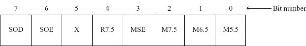
Fig. 18.14 Contents of the accumulator before SIM
Masking of interrupts: Only the LS 4 bits of the accumulator are used for masking or unmasking of interrupts.
| Bit 3: | This is the mask set enable (MSE) bit. If this bit = 0, SIM instruction is not being used for masking or unmasking of interrupts. In such a case, the LS 3 bits of the accumulator are not having any useful information. If MSE bit = 1, the SIM instruction is used for masking or unmasking of interrupts. Then the LS 3 bits provide information about masking or unmasking of interrupts. |
| Bit 2: | This is mask RST7.5 (M7.5) bit. This bit is meaningful only if MSE bit = 1. If MSE = 1 and M7.5 = 0, RST7.5 is unmasked. If MSE = 1 and M7.5 = 1, RST7.5 is masked. |
| Bit 1: | This is M6.5 bit, used for masking/unmasking of RST6.5. It is similar to M7.5 bit. |
| Bit 0: | This is M5.5 bit, used for masking/unmasking of RST5.5. It is similar to M7.5 bit. |
It may be noted that only RST7.5, RST6.5, and RST5.5 can be masked or unmasked using SIM instruction. TRAP and INTR cannot be masked or unmasked using SIM. TRAP is not allowed to be masked because it is the highest priority interrupt. INTR does not need the facility of masking because it is the lowest priority interrupt. After reset of 8085 RST7.5, RST6.5, and RST5.5 interrupts will be in masked condition.
Reset RST7.5 flip-flop: Bit 4 (R7.5) of accumulator is used for resetting to 0 RST7.5 flip-flop output, when SIM instruction is executed. If R7.5 = 0, SIM instruction is not being used for resetting of RST7.5 flip-flop. Thus, if R7.5 = 0, there is no change in the RST7.5 flip-flop output. If R7.5 = 1, the RST7.5 flip-flop gets cleared. This can be visualized from Fig. 18.15, which is actually a part of Fig. 18.17.
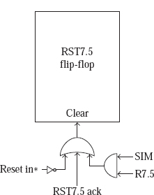
Fig. 18.15 Clearing of RST7.5 flip-flop
In Fig. 18.15, SIM signal is activated when SIM instruction is executed. R7.5 signal is activated when bit 4 (R7.5) of accumulator = 1. So the RST7.5 flip-flop receives logic 1 to its clear input and thus gets cleared when bit 4 of accumulator = 1 and SIM instruction is executed. Alternatively, RST7.5 flip-flop gets cleared when RST7.5 interrupt is recognized by the 8085 or whenever the 8085 is reset.
Serial output of data and SOD pin: Intel 8085 is an 8-bit processor. Thus, it normally sends or receives 8 bits of data at a time. This is known as 8-bit parallel data transfer. In some situations it may not be practical to perform parallel data transfer. Suppose data is to be transmitted over telephone lines, then the 8-bit parallel data will have to be sent out in serial form, one bit after another. Also, we are required to perform serial data transfer when the processor needs to communicate with a serial device, like mouse. Serial communication is much cheaper, because the data transfer takes place on a single line, instead of the eight lines needed in parallel data transfer. However, the speed of communication in serial format is much slower compared with parallel communication. Very few microprocessors provide for on-chip serial communication facility, 8085 being one of them.
Intel 8085 provides SOD (serial output of data) pin and SIM instruction to facilitate serial output of data. From where inside the 8085 does a single bit of information come out on the SOD pin? The MS bit of the accumulator comes out on the SOD pin, when the user commands the 8085 to send out the data. The user commands the 8085 to send out the MS bit of accumulator by making bit 6 of accumulator as 1, and executing the SIM instruction. This can be visualized from Fig. 18.16.
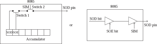
Fig. 18.16 Serial output of data
In Fig. 18.16, switch 1 gets closed when bit 6 of accumulator is at logic 1. Switch 2 gets closed when SIM instruction is executed. So MS bit of the accumulator comes out on SOD pin of 8085 only when bit 6 of accumulator is at logic 1, and SIM instruction is executed. In view of this, the meanings of bits 6 and 7 of the accumulator will be as follows, when we execute SIM instruction.
| Bit 6: | This is the serial output enable (SOE) bit. If this bit = 0, SIM instruction is not being used for serial output of data. In such a case, the MS bit of accumulator is not having any useful information. If SOE bit = 1, the SIM instruction is used for serial output of data. Then the MS bit provides the data to be sent out on the SOD pin of 8085. |
| Bit 7: | This is serial output data (SOD) bit. This bit is meaningful only if SOE bit = 1. If SOE = 1 and SIM instruction is executed, then the SOD bit comes out on the SOD pin of 8085. |
Suppose we have some 8-bit data in the B register, and we want to send it out serially on the SOD pin, starting from the LS bit. Then we have to execute a program that does the following.
- Bring to MS bit of the accumulator a bit from the B register, starting from the LS bit;
- Set to 1, bit 6 of the accumulator;
- Execute the SIM instruction;
- Repeat these steps eight times in a loop.
18.9.3 RIM INSTRUCTION
RIM stands for ‘read interrupt mask’. It is a single-byte instruction. Like the SIM instruction, the RIM instruction is also a multi-purpose instruction. It is used for the following purposes.
- To check whether RST7.5, RST6.5, and RST5.5 are masked or not;
- To check whether interrupts are enabled or not;
- To check whether RST7.5, RST6.5, or RST5.5 interrupts are pending or not;
- To perform serial input of data.
In other words, RIM instruction provides status information about interrupt system and is also used for serial input of data. When RIM instruction is executed, how does the 8085 know which interrupt is masked or unmasked, etc.? The contents of the accumulator after the execution of the RIM instruction provide this information.
Thus, it is essential to look into the accumulator contents after the RIM instruction is executed. The meaning of the various bits of the accumulator after RIM is executed is shown in Fig. 18.17.

Fig. 18.17 Contents of the accumulator after RIM
Mask status of interrupts: The LS 3 bits of the accumulator are used to provide mask status of interrupts. Note that they are not used for masking or unmasking. Masking or unmasking has to be done using the SIM instruction.
| Bit 0: | This is mask RST5.5 (M5.5) bit. If this bit = 1, it means that RST5.5 interrupt has been masked. If M5.5 = 0, RST5.5 interrupt is unmasked. |
| Bit 1: | This is mask RST6.5 (M6.5) bit. If this bit = 1, it means that RST6.5 interrupt has been masked. If M6.5 = 0, RST6.5 interrupt is unmasked. |
| Bit 2: | This is mask RST7.5 (M7.5) bit. If this bit = 1, it means that RST7.5 interrupt has been masked. If M7.5 = 0, RST7.5 interrupt is unmasked. |
Interrupt enable status: Bit 3 of the accumulator provides the status of IE flip-flop after the RIM instruction is executed. If IE = 1, it means that the interrupt system is enabled. This will be the situation if EI instruction is executed sometime prior to the RIM instruction. If IE = 0, it means that the interrupt system is disabled. This will be the situation if some time prior to execution of the RIM instruction, one of the following things have occurred.
- DI instruction was executed;
- Intel 8085 has been reset;
- Intel 8085 has entered an interrupt service subroutine.
Pending interrupt status: Bits 4, 5, and 6 of the accumulator are used to provide pending interrupt status.
| Bit 4: | This is interrupt pending RST5.5 (IP5.5) bit. If this bit = 1, it means that RST5.5 interrupt is pending, waiting to be serviced. This will be the situation when RST5.5 interrupt pin is activated, but RST5.5 is masked, or the interrupt system is disabled. If IP5.5 = 0, the RST5.5 interrupt is not pending. |
| Bit 5: | This is interrupt pending RST6.5 (IP6.5) bit. If this bit = 1, it means that RST6.5 interrupt is pending, waiting to be serviced. If IP6.5 = 0, the RST6.5 interrupt is not pending. |
| Bit 6: | This is interrupt pending RST7.5 (IP7.5) bit. If this bit = 1, it means that RST7.5 interrupt is pending, waiting to be serviced. If IP7.5 = 0, the RST7.5 interrupt is not pending. |
Serial input of data and SID pin: We have already seen the utility of serial communication. Intel 8085 provides SID (serial input of data) pin and RIM instruction to facilitate serial input of data. The logic state on the SID pin of 8085 enters the MS bit of the accumulator when RIM instruction is executed. This can be visualized from Fig. 18.18.
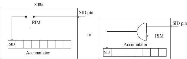
Figure 18.18 Serial input of data
In Fig. 18.18, the switch gets closed when the RIM instruction is executed. So MS bit of the accumulator receives the data present on the SID pin of 8085 when the RIM instruction is executed. In view of this, the meaning of bit 7 of the accumulator will be as follows, after we execute the RIM instruction.
| Bit 7: | This is SID bit. After the RIM instruction is executed, the data on the SID pin of 8085 gets loaded into this bit position. |
Suppose that a serial device is sending some 8-bit data in a serial fashion, starting with the LS bit first. Let us say, we want to receive this information on the SID pin serially and store it in the B register. Then we have to execute a program that does the following.
- Execute the RIM instruction;
- Move the MS bit of the accumulator to a bit position in the B register, starting from the LS bit;
- Repeat these steps eight times in a loop.
Details about the various interrupts of 8085 are summarized in the table that follows.
18.10 HLT INSTRUCTION
HLT is the mnemonic for ‘Halt the microprocessor’ instruction. It is a 1-byte instruction. When this instruction is executed, the 8085 halts further processing and enters Halt state. This is indicated by S1 and S0 output signals becoming 0 0. The 8085 comes out of the Halt state when a valid interrupt occurs. In such a case, it executes the corresponding interrupt service subroutine and then continues with the instruction after the HLT instruction. However, in most programs the HLT instruction is used for terminating the program. Also activation of reset in * causes 8085 to come out of Halt state.
18.11 PROGRAMS USING INTERRUPTS
To acquaint the reader with the usage of interrupts, a few programs that use interrupts are presented in the following.
18.11.1 PROGRAM FOR SIMULATION OF THROWING A DIE
Write an 8085 assembly language program to simulate the throw of a die using an interrupt.
In this program we will have a counter, which counts from 1 to 6, and then repeats the count sequence endlessly in an infinite loop. The throw of the die is simulated by pressing ‘Vect Intr’ key on the keyboard. On the ALS kit when ‘Vect Intr’ key is pressed, RST7.5 pin is activated. It interrupts the counter, with the counter having a random value in the range 1 to 6. The 8085 branches to the RST7.5 ISS. In this ISS, the current value of the counter is displayed in the data field, and the control returns to the main program to continue with the counter operation. Thus, every time the ‘Vect Intr’ key is pressed a random value between 1 to 6 is displayed in the data field, thus simulating the throw of a die.
;FILE NAME DIE.ASM
;Main program to reset RST7.5 flipflop, unmask RST7.5, enable interrupts,
;and count from 1 to 6 endlessly in an infinite loop
       ORG C000H
CURDT: EQU FFF9H
UPDDT: EQU 06D3H
DELAY: EQU 04BEH
MVI A, 00011011B
       SIM              ;Reset RST7.5 flipflop, Unmask RST7.5
       EI               ;Enable interrupt system
;Program segment for an endless counter (1 to 6) loop.
;The 2 NOP instructions are needed because interrupt request
;lines are sensed by 8085 subsequent to JMP BEGIN instruction
;after a short time interval of about 15 clocks. It may be
;better to have 3 NOP instructions to provide margin of safety.

BEGIN:MVI A, 01H
LOOP: NOP
      NOP
      INR A
      CPI 06H
      JNZ LOOP
      JMP BEGIN

   ;RST7.5 ISS to display the counter value

RST75: STA CURDT
       CALL UPDDT ;Display count value in data field
       LXI D, FFFFH
       CALL DELAY ;Generate a delay of 0.5 second
       LDA CURDT
       EI
       RET

;When VECT INTR key is pressed, RST7.5 line is activated. So
;control is shifted to location 7.5 * 8 = 60 = 003CH. This location
;has JMP FFB1H instruction. (For ESA kit there is JMP 8FBFH ). Hence
;it is necessary to write JMP RST75 instruction at location FFB1H.
;This is done by the following 2 instructions.

    ORG FFB1H; For ESA Kit it should be ‘ORG 8FBFH’
    JMP RST75
18.11.2 PROGRAM FOR SIMULATING A STOPWATCH
Write an 8085 assembly language program to simulate a stopwatch to display minutes and seconds in the address field. There should be a provision to stop the stopwatch, with the display continuing to show the time just before the stop command.
In this program we will have a counter, which generates a delay of 1s. After the delay generation, the stopwatch display is incremented by 1s. This is repeated in a loop. To stop the stopwatch, the user is required to press the ‘Vect Intr’ key on the ALS kit. On the ALS kit when ‘Vect Intr’ key is pressed, RST7.5 pin is activated. It interrupts the stopwatch program. The 8085 branches to the RST7.5 ISS. In this ISS, we just have a HLT instruction. Thus, the program comes to a halt, with the display continuing to display the time just before the ‘Vect Intr’ key is pressed.
;FILE NAME STOPWACH.ASM
;PRESSING THE ‘VECT INTR’ KEY STOPS THE STOPWATCH, WITH STATIONARY DISPLAY
        ORG C000H
CURAD: EQU FFF7H
UPDAD:  EQU 06BCH

RESET:  LXI H,0000H
REPEAT: SHLD CURAD
        CALL UPDAD ;Display time present in HL in the address field

        MVI A, 00011011B
        SIM ;Unmask RST7.5, Reset RST7.5 flip flop
        EI ;Enable interrupt system

        CALL DELAY ;Generate a delay of 1 second

        LHLD CURAD
        MOV A, L
        ADI 01H
        DAA ;;;Increment L value in decimal
        CPI 60H
        JZ INC_MIN ;If L = 60, jump to INC_MIN

        MOV L, A
        JMP REPEAT

INC_MIN:

        MVI L, 00H
        MOV A, H
        ADI 01H
        DAA ;;;;Make L = 0, and increment H in decimal
        CPI 60H
        JZ RESET ;If H = 60, jump to RESET

        MOV H, A
        JMP REPEAT

   ;Subroutine to generate a delay of 1 second

   ;To check the proper working of minutes display, load DE with
   ;0444H in this subroutine instead of FFFFH. Then the minutes display
   ;will change every second, so that we can test the proper working in
   ;60 seconds, instead of waiting for 60 minutes.

DELAY:  MVI B, 02H
OUTLOOP:LXI D,FFFFH

INLOOP: DCX D
        MOV A, D
        ORA E
        JNZ INLOOP

        DCR B
        JNZ OUTLOOP
        RET

;RST7.5 Interrupt Service Subroutine

ORG FFB1H ;For ESA Kit it should be ‘ORG 8FBFH’
HLT       ;This is the RST7.5 ISS
18.11.3 FIND THE SQUARE OF A NUMBER USING A LOOK-UP TABLE
Write an 8085 assembly language program to find the square of a single digit (0 to 9) using a look-up table. Display the number and its square in the address field.
The method involves storing a look-up table of squares in RAM, say at location X. Thus, store the following values 00, 01, 04, 09, 16, 25, 36, 49, 64, and 81 in locations starting from X. Then the square of a number is picked up from the look-up table, and displayed in the address field. The program assumes that X address has LS 2 digits as 00H, say C100H.
It waits for the user to press a key in the range 0 to 9. If the user presses any other key, it will remain in the loop. On the ALS kit, whenever the user presses a key other than ‘RESET’ and ‘Vect Intr’, RST5.5 interrupt pin is activated.
;FILE NAME C:ALSLUKUPSQR.ASM

       ORG C100H

  X:   DB 00H, 01H, 04H, 09H, 16H, 25H, 36H, 49H, 64H, 81H

       ORG C000H

CURAD: EQU FFF7H
UPDAD: EQU 06BCH
IBUFF: EQU FFFFH

       MVI A, 0EH ;Load A with 0000 1110B
       SIM ;Unmask RST5.5 i.e. enable keyboard interrupt.

   ;The next 4 instructions check if a key is pressed. If a key is
   ;pressed, RST5.5 pin gets activated but does not interrupt the 8085
   ;as it is in DI state. But RIM instruction execution reveals that
   ;RST5.5 is pending. In such a case, the loop is exited.
 AGAIN:
       DI
       RIM
       ANI 00010000B
       JZ AGAIN ;Stay in this loop till a key is pressed

       EI
       NOP ;RST5.5 interrupts the 8085 now. Only after NOP is
           ;executed, interrupt system is enabled.
  ; So control is transferred to RST5.5 ISS. Details of this ISS
  ; is discussed in a later chapter when Intel 8279 chip is discussed.
  ; Execution of this ISS results in location IBUFF getting loaded
  ; with code of key pressed. Then the control is passed on to the
  ; program segment shown below.

       LDA IBUFF
       CPI 0AH
       JNC AGAIN ;;If code is >= 0AH, jump to AGAIN.

       LXI H, X ;Point HL to the beginning of the look up table.
       MOV L, A ;Load L from A. Thus, point HL to the location which
                ;contains the square of the number input by the user.
MOV A, M ;Load A with the square of the number.
       MOV H, L ;Load H with the number whose square is desired.
       MOV L, A ;Load L with the square of the number.

       SHLD CURAD
       CALL UPDAD ;Display the number and its square.
       JMP AGAIN ;Jump to read the next value from the keyboard.
18.11.4 PROGRAM FOR DECIMAL DOWN COUNTER
Write an 8085 assembly language program to implement a decimal down counter (from 99 to 00). The count should be decremented every time a key (other than RESET and VECT INTR key) is pressed. The count is to be displayed in the data field. The counter operation should repeat endlessly in a cyclic manner.
The program works as follows.
- Load the accumulator with 99.
- Display the count value present in the accumulator in the data field. RST5.5 is unmasked, and the interrupt system is enabled. The monitor routine RDKBD provided by the manufacturer of the kit is executed. This results in a wait for a key depression, and the moment a key is pressed, its code is loaded in the accumulator, and the control returns to the next instruction after CALL RDKBD. In this program, the key code returned by RDKBD routine is not useful. Hence it is ignored. The count value in the accumulator is now decremented by 1 in decimal notation. This is achieved by adding 99, which is 10's complement of 01. Then control is back with the beginning of this para to count from 99 to 00 cyclically.
;FILE NAME C:ALSDNCNTR.ASM

       ORG C000H

CURDT: EQU FFF9H
UPDDT: EQU 06D3H
RDKBD: EQU 0634H

       MVI A, 99H ;Initialize A with 99.

REP:   STA CURDT ;Store A value in CURDT.
       CALL UPDDT ;Display contents of CURDT in data field.

       MVI A, 00001110B
       SIM ;Unmask RST5.5
       EI ;Enable Interrupt system

       CALL RDKBD ;Wait till a key is pressed and load
                  ;the key code in Accumulator, but ignore it.

       LDA CURDT ;Reload A from location CURDT.
       ADI 99H
       DAA ;;Decrement A in decimal notation by
            ;adding 99, which is 10's complement of 01.
       JMP REP ;Jump to REP to display the next count.
18.11.5 PROGRAM FOR DECIMAL DOWN COUNTER (ALTERNATIVE)
Write an 8085 assembly language program to implement a decimal down counter (from 99 to 00). The count should be decremented every time VECT INTR key is pressed. The count is to be displayed in the data field. The counter operation should repeat endlessly in a cyclic manner.
;FILE NAME C:ALSDNCNTR1.ASM

       ORG C000H

CURDT: EQU FFF9H
UPDDT: EQU 06D3H
DELAY: EQU 04BEH

       MVI A, 99H ;Initialize A with 99.
       STA CURDT ;Store A value in CURDT.
       CALL UPDDT ;Display contents of CURDT in data field.

       MVI A, 00011011B
       SIM ;Unmask RST7.5 and reset RST7.5 flip flop
       EI ;Enable Interrupt system

       ;The next 4 instructions forms an infinite loop during
       ;which VECT INTR key is pressed, causing activation of RST7.5

AGAIN: NOP
       NOP
       NOP
       JMP AGAIN

       ;RST7.5 ISS to decrement count value by 1 in decimal
       ;and display it in data field. Then reset RST7.5 flip flop
       ;and enable interrupt system after a delay of 0.5 seconds.

       ;-----------------------------------------------------------

RST75: LDA CURDT
       ADI 99H
       DAA ;Decrement A register value by 1 in decimal

       STA CURDT
       CALL UPDDT ;Display count value in data field

       LXI D, 0000H
       CALL DELAY ;Generate dealy of about 0.5 second
       MVI A, 00010000B
       SIM ;Reset RST7.5 flip flop
       EI ;Enable Interrupt system
       RET

       ;-----------------------------------------------------------

       ;The next 2 instructions store JMP RST75 instruction
       ;at FFB1H on the ALS kit

       ORG FFB1H
       JMP RST75
18.11.6 PROGRAM FOR ADDING 2 NUMBERS INPUT FROM KEYBOARD
Write an 8085 assembly language program to input two 2-digit hexadecimal numbers from the keyboard, add them and output the result in the address field.
;FILE NAME C:ALSAD2INPTS.ASM

       ORG C000H

CURAD: EQU FFF7H
UPDAD: EQU 06BCH
CLEAR: EQU 044AH
GTHEX: EQU 052FH

       MVI A, 0EH
       SIM
       EI ;;;Unmask RST5.5 and enable interrupts

       MVI B, 01
       CALL GTHEX ;;Input a 2 digit number and display in data field

       MOV A, E
       STA C100H ;;Store the 2-digit hex number in C100H

       MVI B, 01
       CALL GTHEX ;;Input a 2 digit number and display in data field

       LDA C100H
       ADD E
       STA CURAD ;;;Add the two numbers and store in CURAD

       JNC SKIP
       MVI A, 01
       STA CURAD+1 ;;;If Carry =1, store 1 in CURAD+1

SKIP:  CALL CLEAR ;Blank the entire display
       CALL UPDAD ;Display sum in address field.
       HLT
In the above program GTHEX and CLEAR monitor routines were used for the first time. The working of these routines are explained below.
GTHEX monitor routine: It stands for GeT HEXadecimal values from keyboard. This routine is used to get 2 hex digits or 4 hex digits from keyboard. Before calling GTHEX, keyboard interrupt (RST5.5) should be enabled by executing the following instructions.
MVI A, 0EH
SIM
EI
If contents of B register is 00H, 4 hex digits are received from the keyboard, and they will be displayed in the address field. They are also stored in DE register pair. If more than 4 digits are entered from the keyboard, only the last 4 digits are accepted. For example, if 345678 is entered, it is treated as 5678. If less than 4 digits are entered, like 345 it is treated as 0345. The user entry is terminated with any of the following valid terminators and the keycode of the terminator will be returned in A register.
EXEC
NEXT
PREV
If contents of B register is 01H, 2 hex digits are received from the keyboard, and they will be displayed in the data field. They are also stored in E register. If more than 2 digits are entered from the keyboard, only the last 2 digits are accepted. For example, if 5678 is entered it is treated as 78. If less than 2 digits are entered, like 5 it is treated as 05. The user entry is terminated with any of the valid terminators as stated above.
On the ALS kit, the GTHEX routine starts at 052FH.
CLEAR monitor routine: This routine blanks out the display in both address and data fields. If contents of B register were 01, a dot will be displayed in the address field. If the contents of register B were 00, even the dot will be blanked out.
All the general purpose registers and Flags register are affected by this routine. On the ALS kit, the CLEAR routine starts at 044AH.
18.11.7 PROGRAM FOR ADDING 4 HEX DIGITS OF A 16-BIT NUMBER
Write an 8085 assembly language program to add 4 hex digits of a 16-bit number input from the keyboard and display the result in the data field.
;FILE NAME C:ALSAD4INPT.ASM

       ORG C000H
CURDT: EQU FFF9H
UPDDT: EQU 06D3H
GTHEX: EQU 052FH
HXDSP: EQU 05A1H
OBUFF: EQU FFFAH

       MVI A, 0EH
       SIM
       EI ;;;Unmask RST5.5 and enable interrupts

       MVI B, 00
       CALL GTHEX ;;Input a 4 digit number and display in address field

       CALL HXDSP ;Store the 4 hex digits in 4 locations starting from OBUFF

       LXI H, OBUUF
       MOV A, M
       MVI C, 03

AGAIN: INX H
       ADD M
       DCR C
       JNZ AGAIN ;When we are out of this loop, A will have the sum.

       STA CURDT
       CALL UPDDT ;Display sum in DATA field.
       HLT
In the above program HXDSP monitor routine was used for the first time. The working of this routine is as explained overleaf.
HXDSP monitor routine: This routine converts the value in DE register pair to 4 unpacked hex bytes and stores them in 4 byte locations starting from OBUFF (output buffer) onwards. The LS unpacked hex byte is stored at OBUFF. On ALS kit, OBUFF is location FFFAH, and HXDSP routine STARTS AT 05A1H. Thus, if (DE) +3456, we will have

- Describe the various methods of parallel data transfer. Bring out their merits and demerits.
- With a neat diagram describe the architecture of the 8085 interrupt system.
- Explain EI and DI instructions.
- Under what circumstances would the 8085 be in the disable interrupt state?
- Describe the means that are used in a kit to reset the microprocessor.
- What happens when the 8085 is reset?
- Describe the action taken by 8085 when INTR is activated.
- Describe the action taken by 8085 when a vectored interrupt pin is activated.
- Explain SIM and RIM instructions.
- Explain the execution of the DAD B instruction.
- Explain how serial communication can be achieved in a 8085 system.
- Write a 8085 program, which displays FF in the data field if RST5.5 interrupt is pending, else it should display 00.
- Write an 8085 assembly language program to implement a decimal down counter (from 99 to 00). The count should be decremented every time VECT INTR key is pressed. The count is to be displayed in the data field. The counter operation should stop after countdown to 00.
- Write an 8085 assembly language program to implement a decimal down counter (from 99 to 00). The count should be decremented every time a key (other than RESET and VECT INTR key) is pressed. It is assumed that RDKBD monitor routine is not available to the user. The count is to be displayed in the data field. The counter operation should stop after countdown to 00.