
30
Advanced Topics In 8051
![]() Interrupt structure of 8051
Interrupt structure of 8051
![]() IE (interrupt enable) register
IE (interrupt enable) register
![]() IP (interrupt priority) register
IP (interrupt priority) register
![]() External interrupts
External interrupts
![]() Timer interrupts
Timer interrupts
![]() Serial port interrupt
Serial port interrupt
![]() Interrupt handing in 8051
Interrupt handing in 8051
![]() Timers of 8051
Timers of 8051
![]() TMOD register
TMOD register
![]() Mode 0 operation of timer/counter
Mode 0 operation of timer/counter
![]() Mode 1 operation of timer/counter
Mode 1 operation of timer/counter
![]() Mode 2 operation of timer/counter
Mode 2 operation of timer/counter
![]() Mode 3 operation of timer/counter
Mode 3 operation of timer/counter
![]() Serial interface
Serial interface
![]() Mode 0 of UART
Mode 0 of UART
![]() Use of Mode 0 to expand I/O port capability
Use of Mode 0 to expand I/O port capability
![]() Mode 1 of UART
Mode 1 of UART
![]() Mode 2 of UART
Mode 2 of UART
![]() Mode 3 of UART
Mode 3 of UART
![]() Architecture of 8051
Architecture of 8051
![]() Structure and operation of ports
Structure and operation of ports
![]() General structure of ports
General structure of ports
![]() Internal structure of P0
Internal structure of P0
![]() Internal structure of P2
Internal structure of P2
![]() Internal structure of P1
Internal structure of P1
![]() Internal structure of P3
Internal structure of P3
![]() Power saving modes of 8051
Power saving modes of 8051
![]() Idle mode
Idle mode
![]() Power down mode
Power down mode
![]() Programming of EPROM in 8751BH
Programming of EPROM in 8751BH
![]() EPROM security
EPROM security
![]() Program verification
Program verification
![]() Erasure of EPROM
Erasure of EPROM
![]() Questions
Questions
This chapter is devoted to the study of advanced topics in 8051, a popular microcontroller chip of the Intel family. In the previous chapter fundamentals of 8051 were dealt with.
 30.1 INTERRUPT STRUCTURE OF 8051
The 8051 can be interrupted from the following five sources.
Two external interrupts INTO* and INT1*;
Two internal timer interrupts T0 and T1;
One internal serial port interrupt.
The interrupt vectors (ISS address) for these interrupt sources are shown as follows.
| INT0* | 0003H |
| Timer0 | 000BH |
| INT1* | 0013H |
| Timer1 | 001BH |
| Serial port | 0023H |
30.1.1 IE (INTERRUPT ENABLE) REGISTER
Each of the interrupt sources can be individually enabled or disabled by programming the IE register. The IE register is an SFR with the address A8H, and is bit addressable, which is shown in Fig. 30.1. It is programmed by the user. The EA (enable all) bit is actually a global disable bit as described below.
EA: 1 = LS 5 bits decide enable/disable of the five interrupts
0 = Disable all five interrupts, irrespective of LS 5 bits

Fig. 30.1 Bit details of IE register
Thus ‘CLR EA’ (or equivalently ‘CLR IE.7’ or ‘CLR AF’) is functionally the same as the DI (disable interrupts) instruction of 8085. If EA = 0, the LS 5 bits are don't-care bits. The meaning of the other bits is as follows when EA = 1.
EX0: 1 = Enable eXternal interrupt0 i.e. INT0*
0 = Disable INT0*
ET0: 1 = Enable Timer0 interrupt
0 = Disable Timer0 interrupt
EX1: 1 = Enable eXternal interrupt 1 i.e. INT1*
0 = Disable INT1*
ET1: 1 = Enable Timer1 interrupt
0 = Disable Timer1 interrupt
ES: 1 = Enable Serial port interrupt
0 = Disable Serial port interrupt
30.1.2 IP (INTERRUPT PRIORITY) REGISTER
Each of the five interrupts can be in one of two priority levels. They are priority levels 1 and 0. Priority level 1 is the higher priority and the user sets these priority levels by programming the IP register. It is a bit-addressable SFR with address B8H. Only the LS 5 bits are meaningful in this register. Figure 30.2 shows the bit details of IP register.
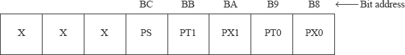
Fig. 30.2 Bit details of IP register
PX0: 1 = 1 level Priority for eXternal interrupt 0 (INT0*)
0 = 0 level priority for INT0*
PT0: 1 = 1 level Priority for Timer0 interrupt
0 = 0 level priority for Timer0 interrupt
PX1: 1 = 1 level Priority for eXternal interrupt 1 (INT1*)
0 = 0 level priority for INT1*
PT1: 1 = 1 level Priority for Timer1 interrupt
0 = 0 level priority for Timer1 interrupt
PS: 1 = 1 level Priority for Serial port interrupt
0 = 0 level priority for Serial port interrupt
If all the five interrupts are set to the same priority level, say level 0, and if several of the interrupts are simultaneously active, the order in which they will be serviced is: INT0*, Timer0, INT1*, Timer1, serial port.
If we want the order of service to be INT0*, INT1*, Timer0, Timer1, serial port, then we have to load IP with xxx00101. However, it is not possible to have some particular sequences of service, for example, INT0*, INT1*, serial port, Timer1, Timer0.
When an interrupt of priority level 0 is being serviced, it can be interrupted by an interrupt of priority level 1, but it cannot be interrupted by another interrupt of priority level 0. When an interrupt of priority level 1 is being serviced, it cannot be interrupted by an interrupt of priority level 1 or priority level 0.
30.1.3 EXTERNAL INTERRUPTS
The external interrupts INT0* and INT1* can be individually programmed to be edge-triggered or level-triggered. This is done by programming the TCON register. TCON is the abbreviation for Timer Control. Although named TCON, it also provides control and status information about the external interrupts. The bit details of TCON register are provided in Fig. 30.3.

Fig. 30.3 Bit details of TCON register
TCON is a bit-addressable register, with SFR address as 88H. Discussion about the LS 4 bits of TCON that provide control and status information about external interrupts, IT0 and ITI (IT for interrupt type) control bits decide whether INT0* and INT1* will be edge-triggered or level triggered inputs as shown in the following. These bits are programmed by the user.
IT0: 1 = INT0* will be negative edge-triggered input
0 = INT0* will be active low level-triggered input
IT1: 1 = INT1* will be negative edge-triggered input
0 = INT1* will be active low level-triggered input
The IE0 and IE1 bits indicate the status of INT0* and INT1* pins. These bits are set or cleared by 8051. IE stands for ‘Interrupt from External source’. For example, IE0 bit is set to 1 by the 8051 when INT0* activation is detected. If INT0* is programmed for edge triggering, IE0 bit is automatically reset to 0 by 8051 when a branch to the ISS at 0003H takes place. If INT0* is programmed for level triggering, IE0 bit is reset to 0 by 8051 only when INT0* input is deactivated. This can be done, for example, by setting to 1 an external flip-flop in the ISS, which deactivates the INT0* request. If this deactivation is not done, the 8051 will again be interrupted after the completion of the ISS.
30.1.4 TIMER INTERRUPTS
The MS4 bits of TCON register shown in Fig. 30.3 provide control and status information about the timers as discussed in the following.
TR0 and TR1 (TR for timer run) bits decide the running of these timers. They provide software control over the running of the timers. There can also be hardware control over the running of timers. Thus, even if a timer is set for run mode by software, it will be in run mode only if some hardware conditions are satisfied, as will be discussed later. In other words, TR bit = 1 is a necessary but not sufficient condition for running the timer. TR0 and TR1 bits are programmed by the user.
TR0: 1 = Timer0 is set to run mode
0 = Timer0 is programmed for stop mode
TR1: 1 = Timer1 is set to run mode
0 = Timer1 is programmed for stop mode
TF0 and TF1 bits indicate the overflow status of Timer0 and Timer1. These bits are set or cleared by 8051. For example, TF0 bit is set to 1 by the 8051 when timer0 overflow occurs. TF0 bit is automatically reset to 0 by 8051 when a branch to the ISS at 000BH takes place. More details about the working of timers is provided later.
30.1.5 SERIAL PORT INTERRUPT
The serial port is used for both transmission and reception. The interrupt status for transmission and reception is provided by TI and RI bits in SCON register. SCON is the abbreviation for serial control. The bit details of SCON register are provided in Fig. 30.4.
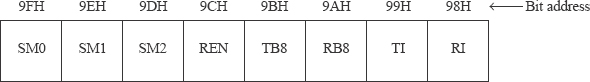
Fig. 30.4 Bit details of SCON register
SCON is a bit-addressable register, with SFR address as 98H. The LS 2 bits of SCON provide status information about serial port interrupts as discussed in the following. TI indicates the transmitter interrupt status, and RI indicates the receiver interrupt status. If any of these 2 bits is a 1, then the 8051 will be interrupted if all the following conditions are met.
- ES bit (enable serial port interrupt) = 1 in IE register
- EA bit (enable all interrupts) = 1 in IE register
- An interrupt of higher or equal priority is currently not being serviced
In such a case, the 8051 branches to the ISS at 0023H. In the ISS, the programmer has to reset the TI and/or RI bit by software. These bits are not automatically reset upon entering the ISS. Further details about the working of serial port and other bits of SCON are provided later. From this discussion on interrupt structure, the 8051 interrupt control system can be visualized as shown in Fig. 30.5.

Fig. 30.5 Interrput control system of 8051
30.1.6 INTERRUPT HANDING IN 8051
A machine cycle consists of six states, S1 to S6. The interrupt flags IE0, IE1, TF0, TF1 of TCON register and RI and TI of SCON register are sampled at the end of S5 in each machine cycle. This is so, even if an instruction needs more than one machine cycle for execution. The samples are polled during the next machine cycle. If one of the interrupt flags is set at the end of S5 of the preceding machine cycle, the polling cycle will find it and the interrupt system will generate an LCALL to the appropriate ISS. This happens provided none of the following is true.
- An interrupt of equal or higher priority level is already in progress.
- The polling cycle is not the final machine cycle in the execution of the instruction in progress.
- The instruction in progress is one of the following:
RETI
Write to IP register
Write to IE register
If any of these conditions is true, LCALL to ISS will not be generated. Condition (b) ensures that the instruction in progress is completed before branching to an ISS. Condition (c) ensures that one more instruction is executed after RETI, or any write to IE and/or IP register, before branching to an ISS.
The hardware generated LCALL pushes the contents of the PC on the stack top, and branches to the appropriate ISS. During this ISS, the 8051 can only be interrupted by a higher priority level interrupt. Thus, if the priority level is already 1, it cannot be interrupted till the ISS is completed. The ISS ends with RETI instruction. The RETI instruction pops to PC from the stack top and additionally informs the 8051 that the ISS is over, which causes the interrupt logic to accept additional interrupt at the same priority level as the one just processed. If the ISS is ended with RET instead of RETI, it would have left the interrupt control system thinking that the interrupt was still in progress.
Single-step operation of 8051: The interrupt structure of 8051 allows single-step execution of a program in a simple way as described in the following. Let us say a key is connected to INT0* pin such that when the key is not pressed, the INT0* pin will be in 0 state. Hence on pressing the key, INT0* becomes 1, and on releasing the key later, it becomes 0 again. The key can be designated as the ‘single-step’ key. Subsequently INT0* interrupt is enabled, INT0* is programmed to be level sensitive, and the ISS for INT0* is terminated with the following code to implement single-step facility. Note that P3.2 bit corresponds to INT0* pin.
LOOP1:    JNB P3.2, LOOP1   ; Remain in LOOP1 till INT0* becomes 1.
LOOP2:    JB P3.2, LOOP2      ; Remain in LOOP2 till INT0* becomes 0.
          RETI                ; Go back and execute 1 instruction.
Although the INT0* pin is at 0 for most part of the single-step routine, it does not interrupt 8051 because the same priority interrupt service (in fact, same interrupt) is in progress. Then at the end of the ISS, it waits for pressing and releasing of ‘single step’ key. After execution of RETI at the end of an ISS, one instruction in the interrupted program will be executed before the 8051 again branches to single step ISS.
30.2 TIMERS OF 8051
There are two 16-bit timer registers in 8051 called Timer0 and Timer1. These timers can be configured to work as times or event counters. In the timer mode, internal machine cycles are counted, whereas in counter mode external events are counted. Thus the only difference between timer and counter is the source for incrementing the timer register.
In the Timer mode the timer register is incremented for every machine cycle consisting of 12 crystal clock cycles. Thus if the 8051 uses 12-MHz crystal, the timer register is incremented once every microsecond in the timer mode. This mode does not use the external timer input pin. The timer input pin is more appropriately called as counter input pin in this book, although Intel refers to it as timer input pin.
In the counter mode, the timer register is incremented for every 1 to 0 transition at the external counter input pin. Every 1 to 0 transition at the external counter input pin is treated as an event. The external counter input pin is sampled once every machine cycle. Hence, to recognize a 1 to 0 transition, atleast two machine cycles are needed. Thus if the crystal frequency is 12 MHz, the maximum count frequency will be 12 MHz/24 = 500 kHz. In other words, for event counting the time duration between events must be atleast 2μs.
In addition to selecting as timer or counter, there are four different modes of operation for these timers/counters. Modes 0, 1, and 2 are the same for both the timers/counters, while mode 3 has different meanings for the two timers/counters. The TMOD register is programmed to configure these timers/counters. Whenever serial port is used for serial communication, specifically in mode 1 and mode 3, Timer1 is used for generating the baud rate. In such a case only Timer0 is available for timer/counter operation. Details about serial port are provided later in this chapter.
30.2.1 TMOD REGISTER
TMOD is an SFR with address 89H, and is non-bit addressable. TMOD is abbreviation for Timer Mode. The bit details of TMOD register and the circuit that controls the running of a timer are provided in Fig. 30.6.
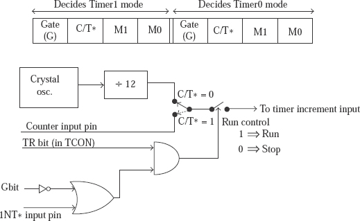
Fig. 30.6 Details of TMOD register and run control of a timer
The user programs all the 8 bits of TMOD, as they are meant for control and not for obtaining status information. The LS 4 bits of TMOD are provided for control of Timer0, and the MS 4 bits of TMOD for control of Timer1, discussed as follows.
C/T*: 1 = Configured for counter operation
0 = Configured for timer operation
M1, M0: 00 = Mode 0 (8-bit timer/counter, with 5-bit prescaler)
01 = Mode 1 (16-bit timer/counter)
10 = Mode 2 (8-bit auto reload timer/counter)
11 = Mode 3 (function depends on if it is for Timer0 or Timer1).
Gate: 0 = TimerX (X = 0 or 1) will be in run mode only if
TRX bit (in TCON register) = 1 (software control)
1 = TimerX will be in run mode only if TRX = 1
and INTX* pin = 1 (hardware control)
This meaning for gate bit is true only when the timer/counter is in mode 0, 1, or 2. The meaning of the gate bit for Timer0 and Timer1 when they are in mode 3 is described later. It is to be noted that in the hardware control of running the timer/counter, external INTX* pin is used. As such, INTX* pin will not be used as an interrupt pin and hence INTX* interrupt should be disabled using IE register.
Example 1
Assume it is desired to use Timer0 as a 16-bit event counter, and Timer1 as an 8-bit auto reload timer. Further, running of these timers is to be controlled by software, then we have to execute the following instruction.
MOV TMOD, #25H; Load TMOD with binary 0 0 10 0 1 01
Timer1 is configured with gate = 0, C/T* = 0, and M1 M0 = 10 indicating that Timer1 works as a timer in mode 2 (8-bit auto reload mode). Also as gate = 0, the timer starts running when TR1 is set to 1 by software. Timer0 is configured with gate = 0, C/T* = 1, and M1 M0 = 01 indicating that Timer0 works as a counter in mode 1 (16-bit counter mode). Also as gate = 0, the timer starts running when TR0 is set to 1 by software.
Example 2
Suppose it is desired to use Timer0 as a 16-bit event counter, and Timer1 as an 8-bit auto reload timer. Further, running of these timers is to be controlled by hardware, then we have to execute the following instruction.
MOV TMOD, #0ADH; Load TMOD with binary 1 0 10 1 1 01
Also execute instruction to make TR1 = 1 and TR0 = 1 in TCON register. Now Timer1 is configured with gate = 1, C/T* = 0, and M1 M0 = 10 indicating that Timer1 works as a timer in mode 2 (8-bit auto reload mode). Also as gate = 1, the timer starts running when external INT1* input is at logic 1, providing hardware control.
Timer0 is configured with gate = 1, C/T* = 1, and M1 M0 = 01 indicating that Timer0 works as a counter in mode 1 (16-bit counter mode). Also as gate = 1, the timer starts running when external INT0* input is at logic 1, providing hardware control. In this example, INT1* and INT0* inputs are not used as external interrupt input pins but used to control the running of Timer1 and Timer0 by an external hardware.
30.2.2 MODE 0 OPERATION OF TIMER/COUNTER
Mode 0 operation is an 8-bit timer/counter with a 5-bit prescaler. Figure 30.7 depicts the mode 0 operation as applied to Timer1. Functionally it is a 13-bit timer/counter, using 5 bits of TL1 register and all the 8-bits of TH1 register.
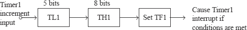
Fig. 30.7 Mode O operation of Timer1
In this case for every 25 = 32 events (in the case of counter operation) or for every 32 machine cycles (in the case of timer operation), the TH1 register is incremented by 1. Finally when TH1 register overflows from FFH to 00, TF1 flag in TCON register is set to 1, and the timer/counter stops. As an example, if TH1 is loaded with F0H, the TF1 flag will be set to 1 after 10H × 32 = 512 machine cycles in the timer mode 0. If the crystal frequency is 12 MHz, this happens after 512 μs. The execution of the following instructions generate an interrupt 512 μs after Timer1 starts running.
MOV TMOD, #00H ; Timer1 in Timer mode 0, with Gate = 0
MOV TH1, #0F0H      ; TH1 (MS byte of Timer1) loaded with F0H
MOV IE, #88H        ; Enable Timer1 interrupt
SETB TR1            ; Set TR1 to 1 in TCON register. Start timer.
30.2.3 MODE 1 OPERATION OF TIMER/COUNTER
Mode 1 operation is a 16-bit timer/counter. Figure 30.8 depicts the mode 1 operation as applied to Timer0.
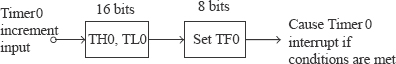
Fig. 30.8 Mode 1 operation of Timer0
In this case, for every event (in the case of counter operation) or for every machine cycle (in the case of timer operation), the TH0–TL0 register pair is incremented by 1. Finally when TH0–TL0 register pair overflows from FFFFH to 0000, TF0 flag in TCON register is set to 1, and the timer/counter stops. As an example, if TH0–TL0 pair is loaded with FFF0H, the TF0 flag will be set to 1 after 10H = 16 machine cycles in the timer mode 1. If the crystal frequency is 12 MHz, this happens after 16 μs. The execution of the following instructions generate an interrupt 16 μs after Timer0 starts running.
MOV TMOD, #01H ; Timer0 in Timer mode 1, with Gate = 0
MOV TL0, #0F0H       ; TL0 (LS byte of Timer0) loaded with F0H
MOV TH0, #0FFH       ; TH0 (MS byte of Timer0) loaded with FFH
MOV IE, #82H         ; Enable Timer0 interrupt
SETB TR0             ; Set TR0 to 1 in TCON register. Start timer.
30.2.4 MODE2 OPERATION OF TIMER/COUNTER
Mode 2 operation is an 8-bit auto reload timer/counter. Figure 30.9 depicts the mode 2 operation as applied to Timer1.
In this case, for every event (in the case of counter operation) or for every machine cycle (in the case of timer operation), the TL1 register content is incremented by 1. Finally when TL1 register overflows from FFH to 00, TF1 flag in TCON register is set to 1. Also TL1 will be reloaded with contents of TH1 and the operation repeats.

Fig. 30.9 Mode 2 operation of Timer1
As an example, if TH1 is loaded with F0H and TL1 is also loaded with F0H, the TF1 flag will be set to 1 after 10H = 16 machine cycles in timer mode 2. If the crystal frequency is 12 MHz, this happens after 16 μs. At this point the TL1 is reloaded with F0H, and the operation repeats thus generating an interrupt every 16 μs. The execution of the following instructions generate an interrupt once every 16 μs after Timer1 starts running.
MOV TMOD, #20H   ; Timer1 in Timer mode 2, with Gate = 0
MOV TL1, #0F0H      ; TL1 (LS byte of Timer1) loaded with F0H
MOV TH1, #0F0H      ; TH1 (MS byte of Timer1) loaded with F0H
MOV IE, #88H        ; Enable Timer1 interrupt
SETB TR1            ; Set TR1 to 1 in TCON register. Start timer.
Timer1 in mode 2 is used for generating the desired baud rate for communication when the serial port is working in mode 1 or mode 3. This aspect will be discussed later.
30.2.5 MODE 3 OPERATION OF TIMER/COUNTER
Mode 3 function is different for Timer0 and Timer1. When Timer0 is operated in mode 3, LS byte of Timer0 (TL0) is used as an 8-bit timer/counter, controlled by the standard Timer0 control bits, Counter0 and INT0* inputs. The MS byte of Timer0 (TH0) is used as an 8-bit timer (not counter) which is controlled by Timer1 control bit TR1. The overflow of TH0 from FFH to 00H causes TF1 (Timer1 overflow) flag to be set. Figure 30.10 depicts the mode 3 operation as applied to Timer0.

Fig. 30.10 Mode 3 operation of Timer0
When Timer1 is operated in mode 3, it simply holds count and stops running. So when Timer0 is in mode 3, Timer1 is generally configured to work in mode 0, 1, or 2. However, Timer1 will not be in a position to interrupt the 8051, as the TF1 flag (Timer1 overflow) is used by TH0 timer. Timer1 is used as Baud rate generator by the serial port very commonly.
The meaning of the gate bit for Timer0 and Timer1 when they are in mode 3 is as follows. Gate bit for Timer0 in mode 3 controls the running of the 8-bit timer/counter TL0, as in the case of mode 0, 1, or 2. The running of the 8-bit timer TH0 is controlled by TR1 bit only. The gate bit for Timer1 in mode 3 does not have any role, as Timer1 in mode 3 only holds count and stops running.
Mode 3 is provided for applications requiring an extra 8-bit timer/counter. When Timer0 is in mode 3, the 8051 has one 8-bit timer using TH0, one 8-bit timer/counter using TL0, and one 16-bit timer/counter using Timer1. It is to be noted that with Timer0 in mode 3, whenever Timer1 operates in mode 0, 1, and 2 the run control for Timer1 is activated when gate bit = 0 or INT1* external input is a logic 1. The run control is deactivated when gate = 1 and INT1* = 0. It is also deactivated whenever Timer1 mode is set to 3.
30.3 SERIAL INTERFACE
The serial port of 8051 can operate in four modes and the operational mode is decided by SM0 and SM1 bits of SCON register. SCON is the abbreviation for serial control. SCON is an SFR with address 98H, and is bit addressable. The bit details of SCON register, which is provided in Fig. 30.4, is reproduced again in Fig. 30.11.
![]()
Fig. 30.11 Bit details of SCON register

30.3.1 MODE 0 OF UART
In this mode the serial data bit stream coming into the 8051 on RXD input pin (P3.0 pin) is received. The data is received treating every 8 bit as one unit. A TXD output pin (P3.1 pin) is used to provide the receive clock. The clock frequency sent out by 8051 on this pin is a fixed frequency of f/12, where f is the crystal frequency. Thus, if the crystal frequency is 12 MHz, a bit is received on RXD pin once every microsecond.
The 8051 has SBUF (serial buffer) register, which is used for serial communication. It is an SFR with address 99H, and is not bit addressable. The SBUF is connected internally to serial port receive register and serial port transmit register, which are not directly accessible by the programmer. The SBUF register is shown in Fig. 30.12. Whenever the 8051 reads the SBUF register, it actually reads from serial port receive register. Similarly, when 8051 writes to SBUF, it will actually be written to serial port transmit buffer.
Reception is initiated when REN (receive enable) bit in SCON = 1, and RI flag bit in SCON = 0. The bits received are accumulated in the serial port receive register, starting with the LS bit. From the point of view of the programmer there is SBUF register, and not serial port receive register. Whenever SBUF is read, it is actually done from serial port receive buffer. Once all the 8 bits are received, the RI flag is set to 1 by the 8051. The user can perform a status check of this bit to perform the read operation from SBUF. In such a case, the user will disable the serial port interrupt. Alternatively, the RI bit can be allowed to interrupt the 8051 which results in a branch to ISS at 0023H provided that:

Fig. 30.12 SBUF register in 8051
- EA and ES bits in IE register are set to 1;
- Higher or equal priority level interrupts are currently not being serviced.
The RI flag must be cleared by software at the end of the ISS.
Mode 0 can also be used for transmitting the 8-bit data present in serial port transmit register in serial fashion on RXD pin, which now acts as an output pin. The serial port transmit register is written by writing to SBUF. The TXD output pin is used to provide the transmit clock. The clock frequency sent out by 8051 on this pin is a fixed frequency of f/12, where f is the crystal frequency. Thus if the crystal frequency is 12 MHz, a bit is transmitted on RXD pin once every microsecond. Transmission is initiated by any instruction which uses SBUF as a destination register, for example, ‘MOV SBUF, A’. The bits are transmitted out from the serial port Transmit register, starting with the LS bit. Once all the 8 bits are transmitted the TI flag is set to 1 by the 8051. The user can perform a status check of this bit to perform the next write operation to SBUF. In such a case, the user will disable the serial port interrupt. Alternatively, the TI bit can be allowed to interrupt the 8051 which results in a branch to ISS at 0023H provided that:
- EA and ES bits in IE register are set to 1;
- Higher or equal priority level interrupts are currently not being serviced.
The TI flag must be cleared by software at the end of the ISS.
As is clear from this discussion, mode 0 is a synchronous mode working in half duplex mode. The most common use of mode 0 is to expand the I/O capability of the 8051 using external shift registers. Mode 0 of UART is also used for high-speed serial data collection. In mode 0 operation of UART, SM2 bit should be 0, as it has no role to play in this mode.
30.3.2 USE OF MODE 0 TO EXPAND I/O PORT CAPABILITY
Serial to parallel shift registers are used for realizing additional output ports. The output mode uses RXD as the serial data output and TXD as the bit-shifting clock for the serial to parallel shift register. Also, an additional output line of 8051 is used to strobe the parallel data out of the shift register. Figure 30.13 depicts the implementation of an external output port.
To implement more output ports, the ‘serial out’ of the first output port must be connected to the ‘serial in’ of the second output port and so on. A typical subroutine to output data to the expansion output port using status check data transfer is provided in the following. It is a general program written to output bytes to several expansion output ports. Before branching to this subroutine, load R0 with the number of expansion ports, and RAM buffer with the data to be output. If four expansion ports are desired, load R0 with 04. Let us say internal RAM locations 20H to 23H are used as RAM buffer. In such a case, location 23H is loaded with the data to be sent to the first expansion port, and location 20H is loaded with the data to be sent to the last expansion port.

Fig. 30.13 Additional output port using mode 0 of UART
MOV SCON, #00H     ; Select mode 0 operation of UART
      CLR ES          ; Disable serial port interrupt
      MOV R1, #20H    ; Load R1 with starting address of RAM buffer
LOOP: CLR TI
      MOV SBUF, @R1   ; Start the serial transmission
WAIT: JNB TI, WAIT    ; Wait in this loop till TI becomes 1
      INC R1          ; Point R1 to next RAM buffer location
      DJNZ R0, LOO    ; Send all the 4 bytes to expansion ports
CLR P1.0
      SETB P1.0       ; Generate 0 to 1 transition on strobe line
      RET
In this program, a RAM buffer from location 20H is used to store the data to be output to the expansion ports. An advantage of the RAM buffer approach is that if the RAM buffer is chosen to reside in on-chip bit-addressable data RAM, then the user can set, clear or test each bit of an expansion port by simply setting, clearing, or testing the corresponding bit in the RAM buffer.
Similarly, parallel to serial shift registers are used for realizing additional input ports. The input mode uses RXD as the serial data input, and TXD as the bit-shifting clock for the parallel to serial shift register. Also an additional output line of 8051 is used to strobe data from the parallel inputs of the external shift register. Figure 30.14 depicts the implementation of an external input port.
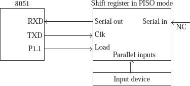
Fig. 30.14 Additional input port using mode 0 of UART
To implement more input ports, the ‘serial in’ of the first input port must be connected to the ‘serial out’ of the second input port and so on. A typical subroutine to input data from the expansion input port is left as an exercise to the reader.
30.3.3 MODE 1 OF UART
Mode 1 is used for asynchronous data transfer. It is a full duplex mode, which means that it can transmit and receive simultaneously. RXD input pin is used for receiving the serial data and accumulating it in the SBUF (actually in serial port receive register). It receives the start bit (which is logic 0), then the 8-data bits (bits 0 to 7) starting from the LS bit, and finally the stop bit (which is logic 1). The received start bit is ignored, the data bits 0 to 7 are loaded in SBUF, and the stop bit is loaded into RB8 (bit 8 of received data) of SCON register.
In this mode the serial data bit stream coming into the 8051 on RXD input pin at the programmed baud rate is received. Its value is determined by the Timer1 (never Timer0) overflow rate. Generally mode 2 of Timer1 (auto reload mode) is used for baud rate generation. The Timer1 interrupt should be disabled in this application. The Timer1 can be configured for ‘timer’ or ‘counter’ operation, but generally it is configured for timer mode. The baud rate is given by the formula
2SMOD 3 f/[32 3 12 × (256–TH1)]
where TH1 is the content of MS byte of Timer1 register and SMOD is the MS bit in PCON (power control) register. PCON is an SFR with address 87H, and is not bit addressable. Whenever SMOD bit = 1, the baud rate is doubled if the serial port is configured for mode 1, 2, or 3. The SMOD bit has no effect on the baud rate of serial port when it is configured for mode 0. More details about PCON register is provided later. Table 30.1 provides the values of baud rates obtained using the above formula when MS nibble of TMOD = 0010 (Timer1 as ‘timer’ in mode 2).
Table 30.1 Baud Rates Generated by Timer1 in mode 1 of UART

Reception is initiated by the incoming start bit if REN bit = 1. Once all the 8-data bits and the stop bit are received, the RI flag is set to 1 by the 8051. In mode 1 operation of UART, if SM2 bit of SCON register is set to 1, then RI bit will not be set to 1, if RB8 = 0. As RB8 holds the stop bit in this mode, it implies that RI bit will not be set to 1 when SM2 = 1 unless a valid stop bit is received by the UART.
The user can perform a status check of the RI bit to perform the read operation from SBUF. In such a case, the user has to disable the serial port interrupt. Alternatively, the RI bit can be allowed to interrupt the 8051, which results in a branch to ISS at 0023H provided that the usual conditions for branching to an ISS are statisfied. The RI flag must be cleared by software at the end of the ISS.
The TXD output pin is used for transmitting the data available in SBUF (actually in serial port transmit register) in serial fashion. It transmits the start bit (which is logic 0), then the 8-data bits (bits 0 to 7) starting from the LS bit, and finally the stop bit (which is logic 1). Transmission is initiated by any instruction that uses SBUF as a destination register.
Once all the 8-data bits and the stop bit are transmitted, the TI flag is set to 1 by the 8051. The user can perform a status check of this bit to perform the next write operation to SBUF. In such a case, the user has to disable the serial port interrupt. Alternatively, the TI bit can be allowed to interrupt the 8051 which results in a branch to ISS at 0023H provided the usual conditions for branching to serial port ISS are satisfied. The TI flag must be cleared by software at the end of the ISS.
Transmission is initiated by any instruction which uses SBUF as a destination register, for example, ‘MOV SBUF, A’. In this mode it transmits the serial data on TXD output pin at the programmed baud rate. Its value is determined by the Timer1 (never Timer0) overflow rate, as was described earlier for receive operation.
30.3.4 MODE 2 OF UART
Mode 2 is also used for asynchrononus data transfer in full duplex mode. RXD input pin is used for receiving the serial data and accumulating it in the SBUF (actually in serial port receive register). It receives the start bit (which is logic 0), then the 8-data bits (bits 0 to 7) starting from the LS bit, a programmed bit 8, and finally the stop bit (which is logic 1). The received start bit is ignored, the data bits 0 to 7 are loaded in SBUF, the programmed bit 8 is loaded into RB8 (bit 8 of received data) of SCON register and the stop bit is ignored.
In this mode it receives the serial data bit stream coming into the 8051 on RXD input pin at the baud rate of f/32 or f/64, where f is the crystal frequency. When SMOD bit in PCON register is 0, the baud rate will be f/64. When SMOD = 1, the baud rate is doubled to f/32.
Reception is initiated by the incoming start bit if REN bit = 1. Once all the 8-data bits, RB8 bit, and stop bit are received, the RI flag is set to 1 by the 8051. In mode 2 operation of UART, if SM2 bit of SCON register is set to 1, then the RI bit will not be set to 1, if RB8 = 0. This feature is useful in multiprocessor communication, as will be described later.
The user can perform a status check of the RI bit to perform the read operation from SBUF. In such a case, the user has to disable the serial port interrupt. Alternatively, the RI bit can be allowed to interrupt the 8051 which results in a branch to ISS at 0023H provided that the usual conditions for branching to an ISS are satisfied. The RI flag must be cleared by software at the end of the ISS.
The TXD output pin is used for transmitting the data available in SBUF (actually in serial port transmit register) in serial fashion. It transmits the start bit (which is logic 0), the 8-data bits (bits 0 to 7) starting from the LS bit, then TB8 bit of SCON register, and finally the stop bit (which is logic 1). Transmission is initiated by any instruction that uses SBUF as a destination register.
Once all the 8-data bits, TB8 bit and the stop bit are transmitted, the TI flag is set to 1 by the 8051. The user can perform a status check of this bit to carry out the next write operation to SBUF. In such a case, the user has to disable the serial port interrupt. Alternatively, the TI bit can be allowed to interrupt the 8051 which results in a branch to ISS at 0023H provided the usual conditions for branching to serial port ISS are satisfied. The TI flag must be cleared by software at the end of the ISS.
The TB8 bit can be loaded by the programmer with a value of 0 or 1, which will be useful in multiprocessor communication, and will be described later. Alternatively, the P flag bit in PSW register can be moved to TB8 bit, which is useful for transmitting data with even parity. In mode 2, the UART transmits the serial data on TXD output pin at the baud rate of f/32 or f/64, based on SMOD bit value.
30.3.5 MODE 3 OF UART
Mode 3 is also used for asynchronous data transfer in full duplex mode. It is the same as mode 2, except the baud rate. The baud rate in mode 3 is variable, like in mode 1.
The RXD input pin is used for receiving the serial data and accumulating in the SBUF (actually in serial port receive register). It receives the start bit (which is logic 0), then the 8-data bits (bits 0 to 7) starting from the LS bit, a programmed bit 8, and finally the stop bit (which is logic 1). The received start bit is ignored, the data bits 0 to 7 are loaded in SBUF, the programmed bit 8 is loaded into RB8 of SCON register, and the stop bit is ignored.
In this mode it receives the serial data bit stream coming into the 8051 on RXD input pin at the programmed baud rate. Its value is determined by the Timer1 (never Timer0) overflow rate. Generally mode 2 of Timer1 (auto reload mode) is used for baud rate generation. The Timer1 interrupt should be disabled in this application. The Timer1 can be configured for ‘timer’ or ‘counter’ operation, but generally it is configured for timer mode. The baud rate is given by the formula
2SMOD ×f/[32 ×12 ×(256 – TH1)]
where TH1 is the content of MS byte of Timer1 register and SMOD is the MS bit in PCON register. Reception is initiated by the incoming start bit if REN bit = 1. Once all the 8-data bits, RB8 bit, and stop bit are received, the RI flag is set to 1 by the 8051. In mode 3 operation of UART, if SM2 bit of SCON register is set to 1, then RI bit will not be set to 1, if RB8 = 0. This feature is useful in multiprocessor communication, as will be described later.
The user can perform a status check of the RI bit to perform the read operation from SBUF. In such a case, the user has to disable the serial port interrupt. Alternatively, the RI bit can be allowed to interrupt the 8051 which results in a branch to ISS at 0023H provided that the usual conditions for branching to an ISS are satisfied. The RI flag must be cleared by software at the end of the ISS.
The TXD output pin is used for transmitting the data available in SBUF (actually in serial port transmit register) in serial fashion. It transmits the start bit (which is logic 0), the 8-data bits (bits 0 to 7) starting from the LS bit, then TB8 bit of SCON register, and finally the stop bit (which is logic 1). Transmission is initiated by any instruction that uses SBUF as a destination register.
Once all the 8-data bits, TB8 bit, and the stop bit are transmitted, the TI flag is set to 1 by the 8051. The user can perform a status check of this bit to perform the next write operation to SBUF. In such a case, the user has to disable the serial port interrupt. Alternatively, the TI bit can be allowed to interrupt the 8051 which results in a branch to ISS at 0023H provided the usual conditions for branching to serial port ISS are satisfied. The TI flag must be cleared by software at the end of the ISS.
The TB8 bit can be loaded by the programmer with a value of 0 or 1, which will be useful in multiprocessor communication, and will be described later. Alternatively, the P flag bit in PSW register can be moved to TB8 bit, which is useful for transmitting data with even parity. In mode 3, serial data is transmitted on TXD output pin at the programmed baud rate. Its value is determined by the Timer1 (never Timer0) overflow rate, as was described earlier for receive operation.
Multiprocessor communication: Modes 2 and 3 of UART provide facility for multiprocessor communications. In these modes data bits 0 to 7 are received in SBUF, and one more bit, called RB8, is received in RB8 bit of SCON register. The UART can be programmed so that RI bit of SCON will be set to 1, causing an interupt to the 8051, only if RB8 = 1. This is done by setting to 1 the SM2 bit in SCON.
When the master 8051 wants to transmit a block of data to one of the several 8051 slaves, it first sends out an address byte that identifies the target slave. For an address byte RB8 bit will be a 1. For a data byte the RB8 bit will be a 0. With SM2 = 1 in the SCON register of each of the slave 8051s, no slave 8051 will be interrupted by a data byte. An address byte will interrupt all slave 8051s. Now each of the slaves can examine the received address byte, and check whether the address is meant for that particular slave. The addressed slave will clear its SM2 bit to 0. The other slaves do not clear the SM2 bit to 0. Thus from now on only the selected slave will receive the data bytes sent by the master.
30.3.6 ARCHITECTURE OF 8051
So far we have discussed in detail the various blocks of 8051. Armed with this knowledge, the detailed architecture of 8051 as shown in Fig. 30.15(a) can be understood easily.

Fig. 30.15 (a) detailed architecture of 8051; (b) Internal structure common to all ports
30.4 STRUCTURE AND OPERATION OF PORTS
All the four ports–PA0, PA1, PA2, and PA3 are bi-directional. Each port circuit consists of a latch, an output driver, and an input buffer. The latches are bit-addressable SFRs with addresses 80H, 90H, A0H, and B0H for the ports P0, P1, P2, and P3 respectively.
The P1 driver receives the data to be sent out from P1 latch. The P0 and P2 drivers receive the information to be sent out either from the port latch or from the memory address register (MAR). The P3 driver receives information from P3 latch or alternate functions. This can be seen from Fig. 30.15(a), which provides the architecture of 8051.
If external program memory is being accessed to fetch a byte of instruction code, the program counter supplies the address to MAR. The MAR register in turn supplies the address to be sent out to the P0 and P2 drivers. Let us say external program memory is being accessed to fetch a byte from a look up table, using indexed addressing. Then the address buffer register will have the computed value of desired memory address. Hence the address buffer register supplies the address to MAR, which in turn supplies the address to be sent out to the P0 and P2 drivers.
If external data memory is being accessed, using Ri (i = 0 or 1) in register indirect addressing mode, then Ri supplies address buffer register (ABR) with LS byte of address to be sent out. From ABR it is passed on to MAR, which in turn sends it to P0 driver. The P2 latch supplies the MS byte of address to P2 driver. If external data memory is being accessed, using DPTR in register indirect addressing mode, then DPTR supplies MAR with address to be sent out, which in turn sends it to P0 and P2 drivers.
In all the above cases, the P0 pins are used for both sending out LS byte of address and sending/receiving 8-bit data. So these pins are being used as AD7-0 pins in time multiplexed mode. The ALE output from 8051 indicates whether address or data is present on AD7-0 pins. ALE stands for ‘address latch enable’. If logic 1 is sent out on ALE, it means 8051 is sending out LS byte of address on P0 pins. An external latch is used to latch this LS byte of address.
In the case of external program memory access, the 8-bit code is received on P0 pins. This information comes to internal bus, and from there is routed to the instruction register (IR), if it is the first or only byte of the instruction. If the data received is the second or third byte of an instruction, they are received in TMP1 and TMP2 registers. IR TMP1, and TMP2 registers are not accessible to the user. In the case of external data memory access, the 8-bit data is received on P0 pins. This information comes to internal bus, and from there is routed to A register.
30.4.1 GENERAL STRUCTURE OF PORTS
All the four port structures are very similar. They differ only in the output driver circuit portion. The internal structure common to all the ports is shown in Fig. 30.15b. The output driver circuit portion for the four ports are shown in Figs. 30.16 to 30.19. The internal structure common to all the ports is discussed in this section. The latch bit, which is a bit of the port SFR, is implemented using D-type flip-flop. When the internal ‘write to latch ’ signal is activated, the latch bit is written with the data bit present on D input, which is connected to the internal bus. The output of the flip-flop will be placed on the internal bus in response to internal ‘read latch ’ signal. The level of the port pin itself is placed on the internal bus in response to internal ‘read pin ’ signal.
In some instructions the port latch information is read, and in some others the port pin information is read. When just reading of the port is desired, it is done from the port pins. If it is desired to read, then modify, and finally write, the information will be read from the port latch. Such instructions will have the destination operand as a port or a port bit. The list of such ‘read-modify-write ’ (RMW) instructions is provided as follows.
ANL (EX. ANL P1, A)
ORL  (EX. ORL P1, A)

XRL  (EX. XRL P1, A)
JBC  (EX. JBC P1.1, LOCN)
CPL  (EX. CPL P1.5)
INC  (EX. INC P1)
DEC  (EX. DEC P1)
DJNZ (EX. DJNZ P1, BACK)

MOV  (EX. MOV P1.5, C)
CLR  (EX. CLR P1.5)
SETB (EX. SETB P1.5)
For example, in ‘ANL P1, A ’ instruction, the 8051 CPU has to read P1 value, then modify it by ANDing it with A contents, and finally write it back to P1. Thus it is a RMW instruction, and so the port latch is read in this instruction. In the ‘Mov P1.5, C ’ instruction, the RMW feature is not obvious. However, the instruction reads all the 8 bits of P1 first, then modifies bit 5 of the port with C value, and then writes the 8 bits back to the port.
The instruction ‘MOV A, P1 ’ is not an RMW instruction, as the destination is not a port. So in this case, A register is loaded with P1 pin information. The reason that RMW instructions access the latch rather than the pin is to avoid a possible misinterpretation of the voltage level at the pin. For example, a port bit might be used to drive the base of a transistor. When a 1 is written to the latch bit, the transistor is turned ‘on ’. Now if the 8051 reads at the pin rather than the latch, it will read the base voltage of the transistor and misinterpret it as a 0. But reading the latch will return the correct value of 1.
30.4.2 INTERNAL STRUCTURE OF P0
The output driver circuit of a pin of P0 is provided in Fig. 30.16.

Fig. 30.16 Output driver circuit of a pin of p0
There is a 2 to 1 multiplexer in P0. One of the inputs is from the complement of a bit in the port latch, while the other input is from an Addr/Data bit of MAR after inversion. If the AD internal control signal shown in the figure is a logic 1, the multiplexer outputs the Addr/Data. If P0 is being used as Addr/Data pins, the internal AD signal will be logic 1. If the Addr/Data bit is at logic 1, the upper FET is on, and the lower FET is off. Thus a 1 is sent out as Addr/Data on the port pin. If the Addr/Data bit is at logic 0, the upper FET off, and the lower FET is on. Thus a 0 is sent out as Addr/Data on the port pin. It is to be noted that there is no need for any external pull up when P0 is being used as Addr/Data pins.
While reading the code byte from external program memory, or reading a data byte from external data memory, the internal AD control signal will be a 0. With the port latch bit at logic 1, both the upper and lower FETs are off. Hence the port pin floats. Now the port pin will be used to receive the code or data byte and the ‘read pin ’ will be activated instead of ‘read latch ’, so that the read will be from the port pin. To facilitate this read operation, the P0 latch will always be written with 1s during access to external program or data memory.
The P0 pins can be used for I/O purposes only if the external program memory or external data memory is not present in the system. In such a case the internal AD control signal will be at logic 0. Then the multiplexer outputs the complement of port latch bit. If the latch bit is at logic 1, the upper FET is off, and the lower FET is also off. Hence the port pin floats. Thus it is seen that P0 does not have internal pull ups when it is used for I/O purposes. So external pull-up resistors have to be used for output operation. Similarly, when the latch bit is at logic 0, the upper FET remains off, and the lower FET is turned on. So the port pin outputs logic 0. If it is desired to use P0 pin as an input pin, the port latch should be written with a 1. Then both the upper and lower FETs are off. Hence the port pin floats, and now it can be used as an input pin.
30.4.3 INTERNAL STRUCTURE OF P2
The output driver circuit of a pin of P2 is provided in Fig. 30.17.

Fig. 30.17 Output driver circuit of a pin of P2
This port uses an active internal pull-up circuit using FETs. The details of this active pull up are not shown for simplicity. There is a 2 to 1 multiplexer in P2. One of the inputs is from a bit of the port latch. The other input is from an Addr bit of MAR. If the AD internal control signal shown in the figure is at logic 1, the multiplexer outputs the Addr. If P2 is being used as Addr pins the internal AD signal will be logic 1. If the Addr bit is a logic 1, the FET is off and the internal active pull up circuit will pull up the port pin to logic 1. Thus a 1 is sent out as Addr on the port pin. If the Addr bit is at logic 0, the internal pull-up circuit will not be active, and the FET is on. Thus a 0 is sent out as address on the port pin. During external memory access, the P2 latch value remains unchanged.
The P2 pins can be used for I/O purposes only if the external program memory or external data memory is not present in the system. In such a case the internal AD control signal will be at logic 0. Then the multiplexer outputs the port latch bit. If the latch bit is at logic 1, the FET is off, and the internal active pull up circuit pulls up the pin output to logic 1. Similarly, when the latch bit is at logic 0, the FET is turned on, and the internal active pull up will not be active. Hence the port pin outputs logic 0. Thus no external pull-up resistors are needed for output operation, whereas for output operation with P0 an external pull-up resistor is needed.
If it is desired to use P2 pin as an input pin, the port latch should be written with a 1. Then the FET is off, and the internal pull-up circuit pulls up the port pin to logic 1. Now the port pin can be used as an input pin. If the external input is at logic 0, the port pin is externally pulled low by this operation.
30.4.4 INTERNAL STRUCTURE OF P1
The internal structure of a pin of P1 is provided in Fig. 30.18.

Fig. 30.18 Output driver circuit of a pin of P1
This port also uses an active internal pull-up circuit using FETs. The details of this active pull up are not shown for simplicity. This port is always available for I/O operations immaterial of the existence of external program memory and data memories.
If the latch bit is at logic 1, the lower FET is ‘off’, and the internal active pulls up circuit pulls up the pin output to logic 1. Similarly, when the latch bit is at logic 0, the lower FET is turned ‘on’, and the internal active pull up will not be active. So the port pin outputs logic 0. Thus no external pull-up resistors are needed for output operation, whereas for those with port 0, external pull-up resistors are needed.
If it is desired to use P1 pin as an input pin, the port latch should be written with a 1. Then the lower FET is ‘off’, and the internal pull-up circuit pulls up the port pin to logic 1. Now the port pin can be used as an input pin. If the external input is at logic 0, the port pin is externally pulled low by this operation.
30.4.5 INTERNAL STRUCTURE OF P3
The output driver circuit of a pin of P3 is provided in Fig. 30.19.

Fig. 30.19 Output driver circuit of a pin of P3
This port also uses an active internal pull-up circuit using FETs. The details of this active pull up are not shown for simplicity. A pin of P3 can be used for I/O operation, if it is not needed for an alternate function. The alternate functions of the P3 pins are listed as follows.
In P3, pins 7 and 6 are used as the alternate output function (AOF) signals RD* and WR* for external data memory, whenever external data memory access is performed. For a P3 pin to be used for generating AOF signal, the corresponding port latch bit must be set to 1. Then the AOF internal signal comes out on the port pin. In case the latch bit is at logic 0, the port pin will be stuck at logic 0, which can be easily seen from the figure for P3 structure.
Assume we want a P3 pin to be used as an alternate input function (AIF) signal. For example, we may want pin 2 of P3 to be used as external interrupt 0 input. Then the corresponding port latch bit must be set to 1. Also the internal AOF signal must be at logic 1. Then the lower FET is ‘off,’ and the internal pull-up circuit pulls up the port pin to logic 1. Now the port pin can be used as an AIF pin. If the external input is a logic 0, the port pin is externally pulled low by this operation. The 8051 senses the value of this external AIF signal by sensing the internal AIF signal, as shown in the figure for P3 structure.
If a P3 pin is not needed for alternate function, the port pin can be used for I/O purposes. In such a case the internal AOF signal will be at logic 1. If the latch bit is at logic 1, the lower FET is ‘off’, and the internal active pull-up circuit pulls up the pin output to logic 1. Similarly, when the latch bit is at logic 0, the lower FET is turned ‘on’, and the internal active pull up will not be active. Hence the port pin outputs logic 0. Thus no external pull-up resistors are needed for output operation.
If it is desired to use P3 pin as an input pin, the port latch should be written with a 1. The internal AOF signal will be at logic 1. Then the lower FET is ‘off’, and the internal pull-up circuit pulls up the port pin to logic 1. Now the port pin can be used as an input pin. If the external input is at logic 0, the port pin is externally pulled low by this operation.
30.5 POWER SAVING MODES OF 8051
8051 is typically implemented using HMOS technology, and is available as 8051H. However, the CHMOS version is also available as 80C51. The CHMOS version is used in applications where power consumption is critical, like data collection in a remote place. The CHMOS version provides two power-reducing modes called the idle mode and the power down mode. The typical current drain from the power supply for 80C51 in the various modes are indicated as follows.
| Normal mode | 18 mA; |
| Idle mode | 2.5 mA; |
| Power down mode | 3 μA. |
30.5.1 IDLE MODE
The chip is programmed to work in idle mode by setting IDL bit of PCON register to 1. PCON is abbreviation for power control. PCON is an SFR with address 87H and is not bit addressable. The bit details of PCON register is provided in Fig. 30.20. Note that in HMOS devices, only SMOD bit, which is already discussed, is implemented in the PCON register.

Fig. 30.20 Bit details of PCON register
Immediately after the IDL bit is set to 1 by an instruction, the device goes to the idle mode. In the idle mode the clock signal is not provided to the CPU core portion. However, the oscillator continues to run, providing the clock to the interrupts, serial port, and timers. This can be seen from Fig. 30.21. Thus the power consumption is greatly reduced, although supply voltage has to be maintained at +5 V. Typically the current drain from the power supply will be only 2.5 mA in idle mode as against 18 mA in normal working mode.

Fig. 30.21 Circuit details of power saving modes
In this mode the program counter, SP, PSW, accumulator, and all other register maintain their data. In other words, the CPU status is preserved fully. The port pins hold the logic values they had at the time the 8051 went to idle mode. The ALE and PSEN* will be held at logic 1. There are two ways to come out of the idle mode. If a valid interrupt occurs, the IDL bit is reset to 0 by the 8051 automatically. Hence the 8051 comes out of the idle mode. It first services the interrupt and then proceeds with the next instruction after the one that put the 8051 into idle mode.
The action to be taken in the ISS may depend on whether the interrupt occurred during normal operation, or in idle mode. This can be taken care of by the two general-purpose flag bits GF1 and GF0 in PCON register. They can be used as truly general-purpose flags, if desired. However, one of these bits is commonly used to indicate if an interrupt occurred during normal operation, or in idle mode. For example, the instruction that sets IDL bit to 1, can also set GF0 to 1. When the idle mode is terminated by an interrupt, the ISS can check the GF0 bit to take appropriate action. The second method of coming out of idle mode is with a hardware reset. The IDL bit is cleared to 0 when reset. The reset redefines all the SFRs, but does not change the on-chip RAM values.
30.5.2 POWER DOWN MODE
The chip is programmed to work in power down mode by setting PD bit of PCON register to 1. Immediately after PD bit is set to 1 by an instruction, the device goes to the power down mode. In the power down mode the clock is not provided to any portion of the 8051. Thus all functions within the 8051 are halted. This can be seen from Fig. 30.21. Hence the power consumption becomes extremely low. But the on-chip RAM and SFR values are held. The port pins output the values held by their respective SFRs. The ALE and PSEN* will be at logic 0. Typically the current drain from the power supply will be only 3μA in power down mode as against 2.5 mA in idle mode.
There is only one way to come out of the power down mode. It is by hardware reset of 8051. The PD bit is cleared to 0 when reset. The reset redefines all the SFRs, but does not change the on-chip RAM values. In the power down mode, the power supply can be reduced to as low as 2 V, but care must be taken to see that power supply is not reduced before going to power down mode. Also power supply should be restored to 5 V before coming out of power down mode.
30.6 PROGRAMMING OF EPROM IN 8751BH
As noted in the previous chapter, 8751 is the EPROM version of 8051. To program the EPROM in 8751, the chip must be running with a 4–6-MHz oscillator. This is because, the internal bus will be used to transfer address and program data to appropriate internal registers. The details of programming of the EPROM vary depending on the 8751 version. They differ with regard to programming voltage value, the width of program pulse, EPROM security features and so on. As such, only programming of the EPROM in 8751BH is described here as a typical example. For other versions of 8751, the reader is advised to go through the manuals of Intel.
The 12-bit address of an EPROM location to be programmed is applied to LS 4 pins of P2 and 8 pins of P1. The data to be written to that location is applied to P0. The connection details for EPROM programming is shown in Fig. 30.22.
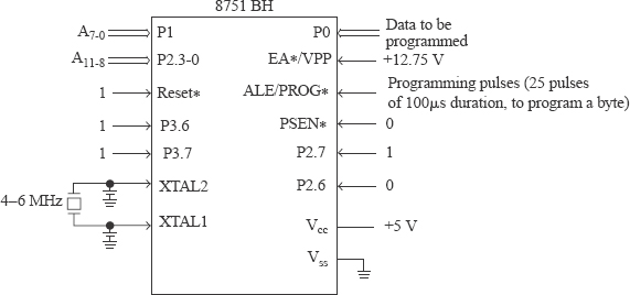
Fig. 30.22 Connection details for EPROM programming
The ALE pin, which is used as an output pin in normal operation, is used as PROG* (program pulse) input during the programming of any part of EPROM, like programming code data, encryption array or lock bits. The encryption array and lock bits are described a little later. The EA* pin, which is tied to 5 V or Gnd during normal operation, is connected to the programming voltage Vpp during programming any part of the EPROM. The programming voltage source should be well regulated and free from glitches. Even a narrow glitch above the specified maximum for programming voltage can cause permanent damage to the device.
The 8751BH uses programming voltage of 12.75 V with a margin of 0.25 V on either side. It uses the faster ‘quick pulse’ programming algorithm. Programming of each byte is done using 25 PROG* pulses, each of 100 μs duration. The gap between each of these 25 PROG* pulses must be atleast 10 μs, as shown in Fig. 30.23. This results in a total programming time of about 13 s for the 4K bytes, taking into account other set up times for programming a byte.

Fig. 30.23 PROG wavefrom used in programming a byte
During any of the EPROM operations like program code byte or verify, reset input is tied to logic 1. The PSEN*, which is an output pin in normal operation, works as an input pin and is tied to logic 0 during any of the EPROM operations. The EA*, MS 2 pins of P2, and MS 2 pins of P3 should be held as indicated in ‘program code data’ row of Table 30.2 for programming a code byte. Pins P2.5 and P2.4 have no role to play in the programming of the EPROM. They are don't-care pins. PROG* is pulsed low 25 times with pulse width of 100 μs to program the code byte into the addressed EPROM location. Normally EA* is held at logic 1, and just before PROG* is to be pulsed EA* is raised to VPP. After PROG* is pulsed 25 times, EA* is returned to logic 1. This completes the programming of 1 byte. The operation is repeated for programming of other bytes.
Table 30.2 Signal Levels For Various EPROM Operations

30.6.1 EPROM SECURITY
In many applications it is desirable that the program memory is secured from software piracy. To facilitate such security 8751BH is provided with two program memory lock schemes, which are encryption array and program lock bits.
Encryption array: The EPROM of 8751BH contains a 32-byte array that can be used for the encryption of code data when verification of code data is attempted. The array is initially unprogrammed (all 1s). The user can program the array and for this purpose the address to be sent will be in the range 00 to 1FH to select an encryption byte. The other pins should be held as indicated in ‘program encryption array’ row of Table 30.2.
The verification procedure sequentially XNORs each byte of the encryption array with a byte of the code. When the last byte in the array is reached, the verification routine restarts with the first byte of the array for the next code byte. Thus the verified code byte will be an encrypted version of the programmed code byte. With the array programmed, the verified bytes can be properly deciphered to obtain the actual programmed code bytes only if all the 32 bytes of encryption array are correctly known.
If the encryption array is not programmed, the XNOR operation produces a verified code byte that is the same as programmed code byte. Another thing to note is that if the programmed code byte is FFH, the verify operation reveals the encryption byte. Thus, if a large block of EPROM is left unprogrammed, the verify operation will reveal the complete encryption array. Hence it is necessary to program unwanted portion of EPROM also with some random values, to ensure protection of the program. It is recommended that whenever encryption array is programmed, atleast one of the program lock bits is also programmed to ensure stiffer protection. It is to be noted that if both the program lock bits are programmed, the on-chip program memory cannot be read out for the purpose of verification.
Program lock bits: Two program lock bits are provided in the EPROM of 8751BH called LB1 and LB2. If both these bits are unprogrammed, the program lock features are not enabled. However, if encryption array is programmed, verification process provides the program bytes in coded form.
To program the LB1 bit, the signals on the various pins should be held at the levels as indicated in ‘program lock bit 1’ row of Table 30.2. If only LB1 bit is programmed, MOVC instructions executed from external program memory are disabled from fetching code byte from EPROM of 8751BH. In this mode, EA* is sampled and latched on reset. Thus, if the device is powered up without a reset, the latch initializes to a random value, and holds that value until reset is activated. To ensure proper functionality of the chip, the internally latched value of EA* must tally with its external input. Also, further programming of EPROM in 8751BH is disabled. In this mode, the verification of program code is possible, but unauthorized users cannot easily decipher the program code, as it will be in encrypted form, if the user programs the encryption array. To program the LB2 bit, the signals on the various pins should be held at the levels as indicated in ‘program lock bit 2’ row of Table 30.2. If both LB1 and LB2 are programmed, the function is the same as in the case where only LB1 is programmed, except that even verification of program code is disabled.
Some versions of 8751, like 87C51, provide three program lock bits—LB1, LB2, and LB3. The function of LB1 and LB2 is the same as in 8751BH. If all the 3 bits are programmed, it denies electrical access by any external means to the on-chip program memory. The device cannot be programmed further and it cannot execute instructions in external program memory. Also, in 87C51, the encryption array is 64 bytes long, double that of 8751BH. Erasing the EPROM deactivates all the lockbits and the device can then be programmed again.
30.6.2 PROGRAM VERIFICATION
If both the program lock bits are programmed, the on-chip program memory cannot be read out for the purpose of verification. In other cases it is possible to read out program memory contents for the purpose of verification of code. The verification can be done after the programming of every byte, or after the completion of the entire programming operation.
The address of the program memory location is applied to LS 4 pins of P2 and 8 pins of P1. The PROG* pin should be held at logic 1 and the other pins as indicated in ‘verify code data’ row of Table 30.2. Note that EA* needs to be held at logic 1. The contents of the addressed EPROM location will come out on P0 pins.
Read signature: Read signature function indicates the manufacturer code and the device code for the chip. The method of reading the signature is similar to verifying code data. The PROG* input is held at logic 1, and the other signals are held as shown in the ‘read signature’ row of Table 30.2. The address to be sent for reading the signature is 30H and 31H. The signature bytes read will be 89H from location 30H, indicating that the manufacturer is Intel and 51H from location 31H, indicating that the chip is 8751BH.
30.6.3 ERASURE OF EPROM
The 8751BH comes in a plastic package without a quartz window. As such, its EPROM contents can only be programmed once and cannot be erased. In other words, the 8751BH contains a PROM. However, most other 8751 versions come with a quartz window, and the EPROM contents in these chips can be erased. Exposing the EPROM to an ultraviolet lamp of 12,000μW/cm2 rating for about 30 min, with the EPROM at a distance of about 2 cm is enough to erase the EPROM. This will erase the complete program, encryption array, and the program lock bits. After the erasure, all bits will be in 1 state.
- Briefly provide an overview of 8051 interrupt structure.
- Describe the function of the IE and IP registers in 8051.
- Provide an overview of the timers in 8051.
- Describe the function of the TCON and TMOD registers.
- Provide an overview of the serial interface of 8051.
- Describe with a neat diagram how mode 0 of UART can be used for the expansion of I/O port capability.
- Provide an overview of the ports in 8051, and their use.
- With a neat diagram describe the working of P1 in 8051.
- Describe the power saving modes of 8051.
- Explain how the EPROM in 8751 is guarded against software piracy.