27
Zilog Z-80 Microprocessor
![]() Comparison of Intel 8080 with Intel 8085
Comparison of Intel 8080 with Intel 8085
![]() Comparison of Intel 8080 with Intel 8085
Comparison of Intel 8080 with Intel 8085
![]() Programmer's view of Z-80
Programmer's view of Z-80
![]() Special features of Z-80
Special features of Z-80
![]() Addressing modes of Z-80
Addressing modes of Z-80
![]() Relative addressing
Relative addressing
![]() Indexed addressing
Indexed addressing
![]() Bit addressing
Bit addressing
![]() Special instruction types
Special instruction types
![]() Rotate and shift instructions
Rotate and shift instructions
![]() Pins of Z-80
Pins of Z-80
![]() Interrupt structure in Z-80
Interrupt structure in Z-80
![]() INT* interrupt
INT* interrupt
![]() NMI* interrupt
NMI* interrupt
![]() Programming examples
Programming examples
![]() Addition of multi-byte numbers
Addition of multi-byte numbers
![]() Exchange of blocks
Exchange of blocks
![]() Block movement without overlap
Block movement without overlap
![]() Instruction set summary
Instruction set summary
![]() Questions
Questions
In the previous chapters Intel 8085 microprocessor was dealt with in depth. This chapter and the next deal with two other very popular 8-bit microprocessors. They are Z-80 microprocessor from Zilog Corporation, and M-6800 microprocessor from Motorola Corporation. This will provide the reader with a comparison of the most popular 8-bit microprocessors.
 27.1 COMPARISON OF INTEL 8080 WITH INTEL 8085
Intel 8080 is the predecessor of both Intel 8085 and Zilog Z-80. In fact, the main people responsible for the development of Intel 8080 left Intel Company and started their own company by the name Zilog. Thus, a brief study of Intel 8080 will enable the reader to appreciate the improvements that have taken place in Intel 8085 and Zilog Z-80.
The functional pin diagrams of Intel 8080 and Intel 8085 are partly provided in Fig. 27.1. The figurealso shows the clock generator chip—Intel 8224 and system controller chip—8228 used with 8080.
The Intel 8224 clock generator provides two-phase clock to the 8080 as shown in Fig. 27.2. The following observations could be made from Fig. 27.1.
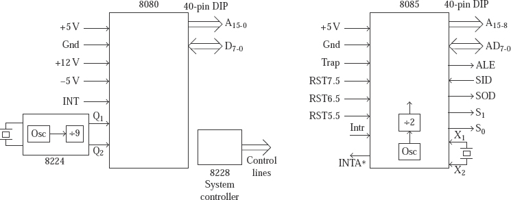
Figure. 27.1 Functional pin diagram of Intel 8080 and Intel 8085
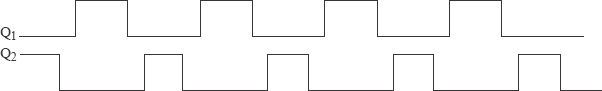
Figure. 27.2 Clock waveform for Intel 8080
| Intel 8080 | Intel 8085 |
| 40-pin DIP | 40-pin DIP |
| 8 data pins D7-0 | 8 multiplexed address-data pins AD7-0 |
| 16 address pins A15-0 | A15-8 and AD7-0. ALE pin added |
| Power supply voltages: +5V, -5V, and +12V | Single power supply of +5V |
| Single interrupt pin INT | TRAP, RST7.5, RST6.5, RST5.5 are extra. |
| No facility for serial communication. | SID and SOD pins, RIM and SIM instructions. |
| 244 opcodes implemented | 246 opcodes implemented. |
| Clock generator chip 8224 needed | Clock generator is internal |
| Internal clock = Crystal frequency/9 | Internal clock = Crystal frequency/2 |
| System controller chip 8228 needed | System controller chip 8228 not needed |
Thus the improvements of 8085 over 8080 are detailed as follows.
- Use of single power supply;
- Intel 8080, 8224, 8228 combined into a single Intel 8085;
- Interrupt structure improved;
- Serial communication provided;
- Two instructions—RIM and SIM, added;
- 4.5 times faster than 8080.
27.2 PROGRAMMER'S VIEW OF Z-80
The programmer's view of Z-80 is provided in Fig. 27.3a and the simplified architecture of Z-80 in Fig. 27.3b.
The Z-80 consists of the following registers, the details of which will be dealt with later.
- Set of standard 8-bit registers—A, B, C, D, E, H, L, and F;
- Alternate set of secondary 8—bit registers—A′, B′, C′, D′, E′, H′, L′, and F′;
- Set of 16-bit address registers—PC, SP, IX, and IY;
- Eight-bit I and R registers.
The alternate set of secondary 8-bit registers cannot be used in Z-80 instructions directly. Thus there are no instructions like ‘move data from B′ register to D′ register’ and ‘move data from C register to B′ register’. The only instructions that make use of these alternate set of registers are EXX and EX AF, AF′.
The EXX exchanges B, C, D, E, H, L with B′, C′, D′, E′, H′, L′. It is an 1-byte instruction with the code D9H. It is executed in just four clock cycles. Thus, it is a very fast way of saving B, C, D, E, H, L registers inside the Z-80 itself.
The EX AF, AF′ exchanges AF with A′F′. It is an 1-byte instruction with the code 08H. It is executed in just four clock cycles. Thus, it is a very fast way of saving A and F registers inside the Z-80 itself.
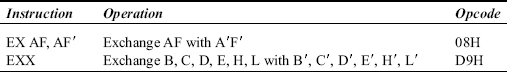
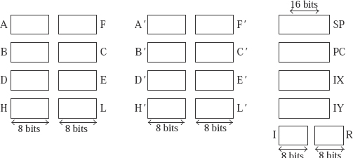
Fig. 27.3a Programmer's view of Z-80
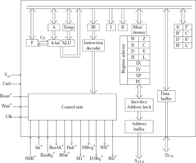
Fig. 27.3b Simplified architecture of Z-80
27.3 SPECIAL FEATURES OF Z-80
Some of the special features of Z-80 are listed in the following.
- 698 opcodes;
- Instruction length: 1 to 4 bytes;
- 1-byte instructions: 202,
- 2-byte instructions: 344,
- 3-byte instructions: 74,
- 4-byte instructions: 78.
- Opcode length: 1 or 2 bytes;
- 1-byte opcodes: 252,
- 2-byte opcodes: 446.
- New addressing modes in comparison with 8085;
- Indexed addressing,
- Relative addressing,
- Bit addressing.
- New instructions in comparison with 8085;
- Block move,
- Block search,
- Powerful I/O instructions,
- Powerful exchange instructions,
- Decimal adjustment after addition or subtraction,
- Instruction to perform program looping,
- Powerful rotate and shift instructions,
- Direct memory access type of instructions.
- Powerful interrupt structure.
27.4 ADDRESSING MODES OF Z-80
All the instructions of Intel 8080 are present in Z-80 and many new ones are provided. Only the RIM and SIM of 8085 are not in Z-80. The mnemonic is different in Z-80 and 8080 for the same instruction in a majority of the cases. For example, ‘DAD B’ instruction of 8080/8085 is the same as ‘ADD HL, BC’ of Z-80 with the same opcode 09H. Thus the programs written for 8080/8085 can be directly run on Z-80, only after the assembly source code of 8080/8085 is translated to machine language. In the following table, the Z-80 mnemonics and the corresponding 8080/8085 mnemonics are provided. In this table, only the instructions that have different mnemonics in Z-80 and 8085 are included. The convention followed in the table is indicated as follows.
d16 = 16-bit immediate data;
a16 = 16-bit address;
a8 = 8-bit address;
r = A, B, C, D, E, H, or L.
‘ADD/ADC A, d8’ stands for ‘ADD A, d8’ and ‘ADC A, d8’;
‘ADD HL, BC/DE/HL/SP’ stands for ‘ADD HL, BC’, ‘ADD HL, DE’ etc.;
‘LD (HL) | r’ stands for ‘LD (HL), r’ and ‘LD r, (HL)’.
As the Z-80 instruction set is a superset of the 8080 instruction set, it has all the addressing modes of 8080/8085. In addition, there are a number of new addressing modes in Z-80. They are: relative addressing, indexed addressing, and bit addressing. These new addressing modes of Z-80 are described as follows.
27.4.1 RELATIVE ADDRESSING
‘JR EXIT’ is an example for an instruction that uses relative addressing. Here JR stands for ‘jump relative’. It is a 2-byte instruction. EXIT is a symbolic memory location to which the branch occurs when ‘JR EXIT’ is executed. Assume EXIT is actual memory location 2357H, and ‘JR EXIT’ instruction is at location 2345H as shown in Fig. 27.4.
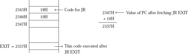
Fig. 27.4 Example for relativeaddressing
By the time the Z-80 fetches the ‘JR EXIT’ instruction, the PC would have been incremented to 2347H. Location EXIT is 10H locations further from location 2347H. Thus the assembler generates an 8-bit signed relative displacement value of 10H. Hence the machine code for the instruction would be ‘18 10’. Here 18H is the opcode for the mnemonic JR, and 10H is the signed displacement corresponding to location EXIT. This 18H happens to be one of the unused opcodes of Intel 8080. The following 12 opcodes were unused in Intel 8080, as only 244 opcodes were implemented: 08H, 10H, 18H, 20H, 28H, 30H, 38H, CBH, D9H, DDH, EDH, and FDH.
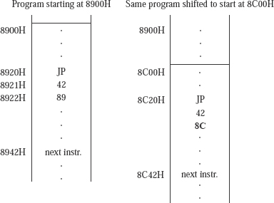
Fig. 27.5a Problem in using absolute jump instruction
If EXIT were to be memory location 2337H, the assembler would have generated an 8-bit signed relative displacement value of F0H, which is nothing but 210H when interpreted as 2's complement signed number. Hence the machine code for the instruction would have been generated as ‘18 F0’. In general, the JR is coded as ‘18 r8’, where r8 is the 8-bit signed displacement.
Advantages of relative addressing: Let us say we have used absolute jump instructions in our program, as shown in Fig. 27.5a. It may be noted that the JMP instruction of 8085 has the mnemonic JP in Z-80. Thus JP stands for absolute jump in Z-80. Assume that our program is stored in memory starting from 8900H and for some reason, we want to shift our program to memory starting from location 8C00H. If the program is simply moved to a new starting location as 8C00H, it will not work properly in that location. It is necessary to modify the addresses that appear in the absolute jump instructions in order that the program works fine in the relocated region. For example, at location 8C20H the instruction should be changed from ‘JP 8942H’ to ‘JP 8C42H’.
Let us suppose we have used relative jump instructions in our program, as shown in Fig. 27.5b. Assume that our program is stored in memory starting from 8900H and for some reason, we want to shift our program to memory starting from location 8C00H. If the program is simply moved to a new starting location as 8C00H, it will work properly in that location. It is not necessary to modify the signed displacements that appear in the relative jump instructions in order that the program works fine in the relocated region. For example, at location 8C20H the instruction remains unchanged as ‘JR 20H’.
Fig. 27.5b Advantage of using Relative jump instruction
Thus, if relative addressing is used for all branch instructions, the program can be easily relocated to any area of memory. Also, the instruction size is only 2 bytes compared to the 3 bytes required in absolute jump instructions. This reduces the code size and improves the execution speed.
Flags Register F: The flags register contents are indicated as follows. It contains only six flags. The other two bits in the flags register are don't care bits.
![]()
The S, Z, AC, and Cy flags have the same purpose that was assigned to them in 8080/8085. As such, the discussion about their role in Z-80 is omitted. The N flag will be discussed during the explanation of DAA instruction, a little later.
The P/O flag stands for ‘parity/overflow’ flag. It is a dual-purpose flag, which works as a P flag when the Z-80 executes any of the following instructions.
Rotate and Shift instructions (Ex. RRC D)
AND, OR, XOR instructions
After the execution of these instructions the P/O flag is set to 1 if there are even number of 1's in the result, otherwise it is reset to 0. The P/O flag works as O flag when the Z-80 executes any of the arithmetic instructions (Ex. ADC D).
Overflow flag: The O flag is meaningful only while working with signed numbers. We just ignore this flag with unsigned numbers. Overflow indicates a wrong answer. The processor sometimes gives a wrong answer when it is performing signed number arithmetic. With unsigned number arithmetic, we always get the correct answer. To drive home the aforementioned points, the meaning of O flag is explained as follows with examples.
Addition of unsigned numbers: If we add 42H and 43H. The result will be 85H with Cy flag value as 0, as shown in the following. If we interpret 42H and 43H as unsigned numbers, the answer is correct. In fact, a microprocessor never gives a wrong answer with unsigned arithmetic.
42H
+43H
85H with carry = 0
Addition of signed numbers: If we add the same two numbers, 42H and 43H, the result will be 85H with Cy flag value as 0, as shown in the following. If we interpret 42H and 43H as signed numbers, the answer is incorrect. A microprocessor sometimes gives a wrong answer with signed arithmetic.
42H (It is positive, as its MS bit is 0)
+ 43H(It is positive, as its MS bit is 0)
85H (It is negative, as its MS bit is 1, and so overflow set to 1)
If we interpret the two numbers as signed numbers, then they are positive numbers, as they start with a 0 in the MS bit position. But the result 85H is negative, as it starts with a 1 in the MS bit position. This is obviously a wrong answer, as the sum of two positive numbers must be positive. Thus, for this example, the O flag will be set to 1.
Let us try to figure out the reason for the occurrence of overflow. The largest positive number using 8 bits is 7FH, and the sum in the example shown is required to be larger than 7FH. So we get a wrong answer. It may be noted that overflow is a possibility, only when we are adding numbers of the same sign, or subtracting numbers of opposite sign.
It may be noted that
O flag value 5 C7 ExOR C6
Where, C6 = Cy generated because of the addition performed at bit position 6.
C7 = Cy generated because of the addition performed at bit position 7.
Thus C7 = Cy flag itself.
Other relative jump instructions: There are four conditional relative jump instructions. The jump takes place or not based on a condition indicated by the value of a corresponding flag in the flags register F. The conditional relative jump instructions are shown in Table 27.1.
Table 27.1 Conditional Relative Jump Instructions
Notice that there are no relative jump instructions that perform a jump based on the value of S flag and P flag which are not commonly needed. However, if conditional jump based on S flag or P flag is desired, one has to use conditional absolute jump instructions.
Finally, there is one more very useful relative jump instruction which is ‘DJNZ r8’. It is also a 2-byte instruction whose opcode is 10H. Its working is as follows.
- It always decrements the contents of B register by 1.
- If the result is non-zero, it performs a backward jump using relative addressing. In DJNZ r8 instructions, r8 is always a negative number.
It is very useful in executing a program segment repetitively for a specified number of times. Thus ‘DJNZ BACK’ instruction is functionally equivalent to the execution of the following two instructions, which occupy a total of 4 bytes.
DEC B
JP NZ BACK
Thus six of the 12 unused opcodes of 8080 are used for the six relative jump instructions in Z-80.
Opcode size for Z-80 instructions: As Z-80 has about 700 opcodes, it may seem that opcodes have to be 10-bits long (as 29 = 512 and 210 = 1,024). This problem is ingeniously solved as follows.
The Z-80 instructions that are common with 8080 (a total of 244) will have the same 8-bit opcode as that of 8080. With 8 bits, a maximum of 28 = 256 opcodes are theoretically possible. So another 12 opcodes are possible. These were not used in 8080. Out of them eight opcodes are used in Z-80 to provide eight new instructions. Six of these new instructions come under relative addressing, discussed earlier. The other two are EXX and EX AF, AF′ which are also discussed earlier.
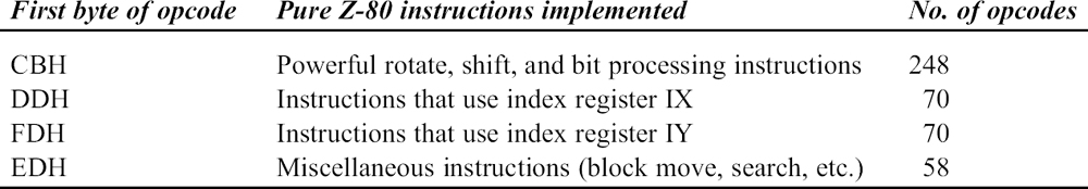
There are still four opcodes remaining which are CBH, DDH, FDH, and EDH. Whenever a Z-80 instruction starts with one of these opcodes it means that it is a pure Z-80 instruction with no parallel in 8080/8085. To exactly find out the new Z-80 instruction, the Z-80 performs second opcode fetch.
The second byte of opcode now indicates the actual new Z-80 instruction. For example, the decoding of 23H by itself, and when preceded by one of the four aforementioned opcodes is shown in Table 27.2.
Table 27.2 Interpretation of Opcode 23H in Z-80
With this scheme, 4 × 256 = 1,024 additional instructions are possible. However only 446 additional instructions are implemented using this scheme.
The new Z-80 instructions that start with the aforementioned four opcodes are briefly indicated in Table 27.3. Instructions that start with the four opcodes as shown in Table 27.3 will have a length of the opcode as 2 bytes.
Table 27.3 Implementation of Pure Z-80 Instructions
27.4.2 INDEXED ADDRESSING
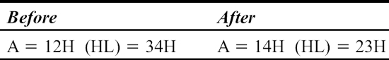
‘ADD A, (IX120H)’ is an example for an instruction that uses indexed addressing. The execution of this instruction results in the addition of A contents with the contents of a memory location. The address of the memory location is partly provided in IX register. The other part of the memory address is provided in the instruction itself. In the aforementioned instruction, the other part of the address is 20H. The 20H in this instruction is commonly called the displacement. It is 8 bits in size, and is an unsigned number. It is denoted as ‘d8’ in general to indicate displacement of 8 bits size. Indexed addressing is a very powerful addressing mode and is very convenient to access data values in a table.
Example: Assume that A has 30H before the execution of this instruction and the IX content is 8900H. This is interpreted as part of the memory address. The other part of the address provided in the instruction is 20H. Thus the complete memory address is 8920H. If the contents of this location are 35H, then 35H is added to A register contents. The result will be stored in A register. Thus, A contents are changed to 65H after the execution of the instruction. It is indicated diagrammatically as follows.
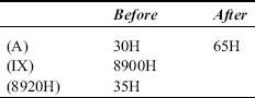
ADD A, (IX120H) is a 3-byte instruction with the opcode DD 86 20H.
DDH indicates that it is a pure Z-80 instruction that uses IX register.
86H indicates that the instruction is ‘ADD A, (IX1d8)’.
20H indicates that the displacement is 20H.
 27.4.3 BIT ADDRESSING
If the instruction set of Z-80 does not provide bit addressing, then the following five instructions are to be executed for setting bit 3 of B register. In 8085 this method is used for setting bit 3 of B register.
| PUSH AF; | It is PUSH PSW of 8085. Save A and F on stack top |
| LD A, B; | It is MOV A, B of 8085. Move B contents to A |
| OR 08H; | It is ORI 08H of 8085. Set bit 3 of A register |
| LD B, A; | It is MOV B, A of 8085. Save result in B register |
| POP AF; | It is POP PSW of 8085. Restore A and F values |
Bit SET instruction: The Z-80 provides a powerful bit addressing mode. An example for an instruction that uses bit addressing is ‘SET 3, B’. The execution of this single instruction results in setting bit 3 of B register to the 1 state. This amply demonstrates the power of bit addressing mode.
‘SET 3, B’ is a 2-byte instruction with the opcode CB D8H.
CBH indicates that it is a pure Z-80 instruction involving shift, rotate, or bit processing.
D8H = 11 011 000 indicates that the instruction is ‘SET 3, B’ because of the following.
11 indicates that it is a SET instruction.
N = nnn = 011 indicates that bit 3 is to be set.
R = rrr = 000 indicates that register B is to be used in the instruction.
Similarly, the execution of ‘SET 3, (IY130H)’ instruction results in setting bit 3 of a memory location. The address of the memory location is partly provided in IY register. The other part of the memory address is 30H, which is provided in the instruction itself.
If IY content is 8900H, it is interpreted as part of the memory address. The other part of the address provided in the instruction is 30H. Thus the complete memory address is 8930H. Assume that the contents of this location is 35H = 0011 0101, with bit 3 value as 0. After the execution of this instruction, the contents of memory location 8930H change to 3DH = 0011 1101, indicating that bit 3 has been set to 1.
‘SET 3, (IY+30H)’ is a 4-byte instruction with the opcode FD CB 30 DEH.
FDH indicates that it is a pure Z-80 instruction involving IY register.
CBH indicates that it is a pure Z-80 instruction involving shift, rotate, or bit processing.
30H provides the displacement value d8 in the indexed addressing mode.
DEH = 11 011 110 indicates that the instruction is ‘SET 3, (IY+30H)’ because of the following.
11 nnn 110 indicates that it is ‘SET N, (Iz+d8)’ instruction, where Iz = IX or IY
N = nnn = 011 indicates that bit 3 is to be set.
From these examples, it is clear that there are two general formats for the SET instruction. They are ‘SET N, R’ and ‘SET N, (Iz+d8)’, where
N = bit number, a value in the range 0-7
R = A, B, C, D, E, H, L, or (HL) that stands for memory pointed by HL.
Iz = IX or IY
d8 = 8-bit unsigned displacement.
Bit RES instruction: The other bit processing instructions provided in the instruction set of Z-80 are the RES and BIT instructions. RES stands for reset a specified bit. BIT stands for test a specified bit.
The execution of ‘RES 4, C’ results in resetting bit 4 of register C to the 0 state. It is a 2-byte instruction. Similarly, the execution of ‘RES 3, (IY+30H)’ instruction results in resetting bit 3 of a memory location. The address of the memory location is partly provided in IY register. The other part of the memory address is 30H. ‘RES 3, (IY+30H)’ is a 4-byte instruction. The two general formats for the RES instruction are ‘RES N, R’ and ‘RES N, (Iz+d8)’.
BIT instruction: The execution of ‘BIT 4, C’ results in testing bit 4 of register C. If the bit value is 0, then the Z flag is set to 1, otherwise it is reset to 0. The instruction execution does not alter the bit value. The BIT instruction is generally followed by ‘JR NZ r8’ or ‘JR Z r8’ instruction. ‘BIT 4, C’ is a 2-byte instruction.
Similarly, the execution of ‘BIT 3, (IY+30H)’ instruction results in testing bit 3 of a memory location. The address of the memory location is partly provided in IY register. The other part of the memory address is 30H. ‘BIT 3, (IY+30H)’ is a 4-byte instruction. The two general formats for the BIT instruction are ‘BIT N, R’ and ‘BIT N, (Iz+d8)’.
27.5 SPECIAL INSTRUCTION TYPES
DAA Instruction: The DAA instruction of 8085 always adds 00H, 06H, 60H, or 66H depending on the contents of A register and the status of Cy and ACy flags. In other words, it is functionally same as ADI 00H/06H/60H/66H. Intel gave the expansion for ‘DAA’ instruction of 8085 as ‘Decimal Adjust Accumulator’. But a more appropriate expansion would have been ‘Decimal Adjust after Addition’, because, the DAA instruction of 8085 is supposed to be used for arriving at correct decimal answer only after addition of two 2-digit BCD numbers. It should not be used for arriving at correct decimal answer after subtraction of two 2-digit BCD numbers. In fact, there is no single instruction in 8085 to arrive at correct decimal answer after subtraction of two 2-digit BCD numbers.
As an example, assume that we want to compute 45 – 28. The required answer is 17. If the subtraction were done treating the numbers as hexadecimal, the accumulator contents would be 1DH. Then the execution of DAA instruction of 8085 results in addition of 06H, to get the BCD answer as 23. This is an incorrect result. To get the correct result of 17, 06H would have to be subtracted from 1DH, but there is no single instruction in 8085 to do this.
Now consider Z-80, which has DAA instruction standing for ‘Decimal Adjust Accumulator’. It is indeed a very apt expansion in the case of Z-80 because, the DAA instruction of Z-80 can be used for arriving at correct decimal answer immaterial of addition or subtraction of two 2-digit BCD numbers. The DAA instruction of Z-80 is functionally the same as
ADD A 00H/06H/60H/66H if addition was performed prior to execution of DAA
SUB 00H/06H/60H/66H if subtraction was performed prior to execution of DAA
As an example, assume that we want to compute 45 – 28. The required answer is 17. If the subtraction were done treating the numbers as hexadecimal, the accumulator contents would be 1DH. Then the execution of DAA instruction of Z-80 results in subtraction of 06H, to get the correct BCD answer as 17.
But how does Z-80 know whether to add 06H or subtract 06H to arrive at the correct answer in the aforementioned example? This problem is solved by the status of N flag. The value of the N flag is decided by the operation performed by Z-80. It has nothing to do with the result of the operation. Other flags, like Cy, are affected by the result of the operation.
- The N flag is reset to 0 if 8-bit add or increment operation is performed.
- The N flag is set to 1 if 8-bit subtract or decrement operation is performed.
The action taken by Z-80 when DAA instruction is executed depends on the
- value of N flag;
- contents of the accumulator;
- contents of Cy and AC flags.
To summarize, the DAA instruction of Z-80 is functionally the same as
ADD A 00H/06H/60H/66H if N flag = 0
SUB 00H/06H/60H/66H if N flag = 1
LDI Instruction: Assume that we want to move the contents of memory location C200H to memory location C100H. It could be done using the following program segment without altering the contents of register A.
| LD HL, C200H; | Same as LXI H, C200H of 8085 |
| LD DE, C100H; | Same as LXI D, C100H of 8085 |
| PUSH AF; | Same as PUSH PSW of 8085 |
| LD A, (HL); | Same as MOV A, M of 8085 |
| LD (DE), A; | Same as STAX D of 8085 |
| POP AF; | Same as POP PSW of 8085 |
An easier and more efficient method in Z-80 would be to use the LDI instruction. The execution of this instruction results in the following:
- Move contents of memory pointed by HL to memory pointed by DE.
- Increment HL and DE contents by 1.
- Decrement BC contents by 1.
‘LDI’ stands for LoaD (from memory pointed by HL to memory pointed by DE) and then Increment HL and DE (BC is always decremented). It is a 2-byte instruction with the opcode ED A0H where:
- EDH indicates that it is a pure Z-80 instruction.
- A0H indicates that it is LDI instruction.
Thus, to move the contents of memory location C200H to memory location C100H, the easier option would be:
LD HL, C200H
LD DE, C100H
LDI
A more powerful and useful instruction is the LDIR instruction.
LDIR Instruction: Assume that we want to move a block of information of size 6 bytes starting at location C200H to the block at location C100H. If the processor is 8085, we are required to execute a program to achieve this. Such a program was provided in Sect. 15.4 of Chap. 15. A similar program could be written in Z-80 also, but it can be made more simple and efficient using the block move instruction LDIR provided in Z-80.
The execution of the LDIR instruction results in the following:
- Move contents of memory pointed by HL to memory pointed by DE.
- Increment HL and DE contents by 1.
- Decrement BC contents by 1.
- Repeat steps 1, 2, and 3 if BC content is not 0000H.
‘LDIR’ stands for LoaD (from memory pointed by HL to memory pointed by DE), then Increment HL and DE (BC is always decremented), and Repeat the operation (till BC becomes zero). It is a 2-byte instruction with the opcode ED B0H where:
- EDH indicates that it is a pure Z-80 instruction.
- B0H indicates that it is LDIR instruction.
Thus, to move the contents of a block of 6 bytes of memory starting at location C200H to memory location C100H, the easier option would be:
LD HL, C200H
LD DE, C100H
LD BC, 0006H
LDIR
LDD Instruction: An alternative method to move the contents of memory location C200H to memory location C100H would be to use the LDD instruction. The execution of this instruction results in the following:
- Move contents of memory pointed by HL to memory pointed by DE.
- Decrement HL and DE contents by 1.
- Decrement BC contents by 1.
‘LDD’ stands for LoaD (from memory pointed by HL to memory pointed by DE) and then Decrement HL and DE (BC is always decremented). It is a 2-byte instruction.
Thus, to move the contents of memory location C200H to memory location C100H, an alternative easier option would be:
LD HL, C200H
LD DE, C100H
LDD
A more powerful and useful instruction is the LDDR instruction.
LDDR Instruction: Assume that we want to move a block of information of size 6 bytes starting at location C200H to the block at location C100H. An alternative to LDIR instruction is the equally simple and efficient instruction LDDR provided in Z-80.
The execution of the LDDR instruction results in the following:
- Move contents of memory pointed by HL to memory pointed by DE.
- Decrement HL and DE contents by 1.
- Decrement BC contents by 1.
- Repeat steps 1, 2, and 3 if BC content is not 0000H.
‘LDDR’ stands for LoaD (from memory pointed by HL to memory pointed by DE), then Decrement HL and DE (BC is always decremented), and Repeat the operation (till BC becomes zero). It is a 2-byte instruction.
Thus, to move the contents of a block of 6 bytes of memory starting at location C200H to memory location C100H, the equally easy option using LDDR would be:
LD HL, C205H
LD DE, C105H
LD BC, 0006H
LDDR
CPI Instruction: The execution of CPI instruction results in the following:
- Compare A register contents with contents of memory pointed by HL.
- Increment HL contents by 1.
- Decrement BC contents by 1.
‘CPI’ stands for ComPare (register A contents with contents of memory pointed by HL) and then Increment HL (BC is always decremented). It is a 2-byte instruction with the opcode ED A1H where:
- EDH indicates that it is a pure Z-80 instruction.
- A1H indicates that it is CPI instruction.
A more powerful and useful instruction is the CPIR instruction.
CPIR Instruction: Assume that we want to search for a specific byte value of 23H in a block of information of size 6 bytes starting at location C200H. If the processor is 8085, we are required to execute a program to perform this linear search operation. Such a program is provided in Sect. 16.1 of Chap. 16. A similar program could be written in Z-80 also, but it can be made more simple and efficient using the block search instruction CPIR provided in Z-80.
The execution of the CPIR instruction results in the following:
- Compare A register contents with contents of memory pointed by HL.
- Increment HL contents by 1.
- Decrement BC contents by 1.
- Repeat steps 1, 2, and 3 if BC content is not 0000H.
‘CPIR’ stands for ComPare (A register contents with contents of memory pointed by HL), then Increment HL (BC is always decremented), and Repeat the operation (till BC becomes zero). It is a 2-byte instruction with the opcode ED B1H where:
- EDH indicates that it is a pure Z-80 instruction.
- B1H indicates that it is CPIR instruction.
Thus, to search for a specific byte value of 23H in a block of information of size 6 bytes starting at location C200H, the easier option would be:
LD HL, C200H
LD A, 23H
LD BC, 0006H
CPIR
The Z flag is set to 1 if the byte value 23H is found anywhere in the block. The location in the block where the byte is found is pointed by HL. If the byte were not found in the block, then the Z flag would be reset to 0. Thus ‘JR NZ r8’ or ‘JR Z r8’ instruction normally follows the CPIR instruction.
CPD Instruction: The execution of CPD instruction results in the following:
- Compare A register contents with contents of memory pointed by HL.
- Decrement HL contents by 1.
- Decrement BC contents by 1.
‘CPD’ stands for ComPare (A register contents with contents of memory pointed by HL) and then Decrement HL (BC is always decremented). It is a 2-byte instruction. A more powerful and useful instruction is the CPDR instruction.
CPDR Instruction: Assume that we want to search for a specific byte value of 23H in a block of information of size 6 bytes starting at location C200H. For this purpose the CPIR instruction could be used. An equally simple and efficient method is using the block search instruction CPDR in Z-80.
The execution of the CPDR instruction results in the following:
- Compare A register contents with contents of memory pointed by HL.
- Decrement HL contents by 1.
- Decrement BC contents by 1.
- Repeat steps 1, 2, and 3 if BC content is not 0000H.
‘CPDR’ stands for ComPare (A register contents with contents of memory pointed by HL), then Decrement HL (BC is always decremented), and Repeat the operation (till BC becomes zero). It is a 2-byte instruction.
Thus, to search for a specific byte value of 23H in a block of information of size 6 bytes starting at location C200H, an equally easier option would be:
LD HL, C205H
LD A, 23H
LD BC, 0006H
CPDR
‘JR NZ r8’ or ‘JR Z r8’ instruction normally follows the CPDR instruction.
IN reg, (C) Instruction: Assume that we want data to be moved from input port number 56H to B register. This could be done using the following program segment.
PUSH AF
IN A, (56H); Same as IN 56H of 8085
LD B, A
POP AF
In an 8085-based system, this method was the only way to move data to B register from an I/O port. However, in a Z-80-based system there is a simpler and more efficient method using ‘IN reg, (C)’ instruction. Here, ‘reg’ refers to any of the registers A, B, C, D, E, H, or L. For example, the execution of ‘IN B, (C)’ instruction results in: Move data to register B from input port whose address is provided in C register.
In this type of instruction, C register has a special role to play. Only C register is allowed to have the 8-bit address of the I/O port. Thus to move data from input port number 56H to B register, it is enough to execute the following two instructions.
LD C, 56H
IN B, (C)
IN B, (C) is a 2-byte instruction with the opcode ED 40H where:
EDH indicates that it is a pure Z-80 instruction.
40H = 01 000 000 indicates that it is ‘IN B, (C)’ instruction because of the following.
01 rrr 000 indicates that it is ‘IN reg, (C)‘ instruction.
rrr 5 000 indicates that register B is to be used in the instruction.
INI Instruction: The execution of INI instruction results in the following:
- Move data to memory location pointed by HL from input port whose address is provided in C register.
- Increment HL contents by 1.
- Decrement B contents by 1.
‘INI’ stands for INput (from input port whose address is provided in C register to memory pointed by HL) and then Increment HL (B is always decremented). It is a 2-byte instruction. A more powerful and useful instruction is the INIR instruction.
INIR Instruction: The execution of INIR instruction results in the following:
- Move data to memory location pointed by HL from input port whose address is provided in C register.
- Increment HL contents by 1.
- Decrement B contents by 1.
- Repeat steps 1, 2, and 3 if B content is not 00H.
‘INIR’ stands for INput (from input port whose address is provided in C register to memory pointed by HL), then Inecrement HL (B is always decremented). and Repeat the operation (till B becomes zero). It is a 2-byte instruction, which is used for reading a string of bytes from an input port and storing in consecutive memory locations. It is a DMA type of instruction, as the port directly communicates with memory in this case.
IND Instruction: The execution of IND instruction results in the following:
- Move data to memory location pointed by HL from input port whose address is provided in C register.
- Decrement HL contents by 1.
- Decrement B contents by 1.
‘IND’ stands for INput (from input port whose address is provided in C register to memory pointed by HL) and then Decrement HL (B is always decremented). It is a 2-byte instruction. A more powerful and useful instruction is the INDR instruction.
INDR Instruction: The execution of INDR instruction results in the following:
- Move data to memory location pointed by HL from input port whose address is provided in C register.
- Decrement HL contents by 1.
- Decrement B contents by 1.
- Repeat steps 1, 2, and 3 if B content is not 00H.
‘INDR’ stands for INput (from input port whose address is provided in C register to memory pointed by HL), then Decrement HL (B is always decremented), and Repeat the operation (till B becomes zero). It is a 2-byte instruction, which is used for reading a string of bytes from an input port and storing in consecutive memory locations. It is a DMA type of instruction, as the port directly communicates with memory in this case.
OUT (C), reg Instruction: Assume that we want data to be moved from B register to output port number 56H. This could be done using the following program segment.
PUSH AF
LD A, B
OUT (56H), A ; Same as OUT 56H of 8085
POP AF
In an 8085-based system, this method was the only way to move data from B register to an I/O port. However, in a Z-80-based system there is a simpler and more efficient method using ‘OUT (C), reg’ instruction. Here, ‘reg’ refers to any of the registers A, B, C, D, E, H, or L. For example, the execution of ‘OUT (C), B’ instruction results in the following:
- Move data from B register to output port whose address is provided in C register.
- Only C register is allowed to have the 8-bit address of the I/O port.
Thus to move data from B register to output port number 56H, it is enough to execute the following two instructions.
LD C, 56H
OUT (C), B
‘OUT (C), B’ is a 2-byte instruction.
OUTI Instruction: The execution of OUTI instruction results in the following:
- Move data from memory location pointed by HL to output port whose address is provided in C register.
- Increment HL contents by 1.
- Decrement B contents by 1.
‘OUTI’ stands for OUTput (from memory pointed by HL to output port whose address is provided in C register) and then Increment HL (B is always decremented). It is a 2-byte instruction. A more powerful and useful instruction is the OTIR instruction.
OTIR Instruction: The execution of OTIR instruction results in the following:
- Move data from memory location pointed by HL to output port whose address is provided in C register.
- Increment HL contents by 1.
- Decrement B contents by 1.
- Repeat steps 1, 2, and 3 if B content is not 00H.
‘OTIR’ stands for OuTput (from memory pointed by HL to output port whose address is provided in C register), then Increment HL (B is always decremented), and Repeat the operation (till B becomes zero). It is a 2-byte instruction, which is used for sending a string of bytes from consecutive memory locations to an output port. It is a DMA type of instruction, as memory communicates directly with the port in this case.
OUTD Instruction: The execution of OUTD instruction results in the following:
- Move data from memory location pointed by HL to output port whose address is provided in C register.
- Decrement HL contents by 1.
- Decrement B contents by 1.
‘OUTD’ stands for OUTput (from memory pointed by HL to output port whose address is provided in C register) and then Decrement HL (B is always decremented). It is a 2-byte instruction. A more powerful and useful instruction is the OTDR instruction.
OTDR Instruction: The execution of OTDR instruction results in the following:
- Move data from memory location pointed by HL to output port whose address is provided in C register.
- Decrement HL contents by 1.
- Decrement B contents by 1.
- Repeat steps 1, 2, and 3 if B content is not 00H.
‘OTDR’ stands for OuTput (from memory pointed by HL to output port whose address is provided in C register), then Decrement HL (B is always decremented), and Repeat the operation (till B becomes zero). It is a 2-byte instruction.
This instruction is used for sending a string of bytes from consecutive memory locations to an output port. It is a DMA type of instruction, as memory communicates directly with the port in this case.
27.5.1 ROTATE AND SHIFT INSTRUCTIONS
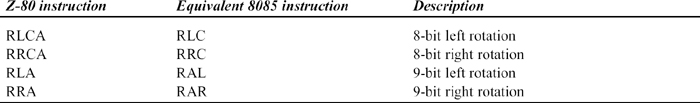
Rotate instructions: The rotate instructions of Z-80 that were available in 8085 also are shown in Table 27.4.
Table 27.4 Rotate Instructions of Z-80 that were present in 8085
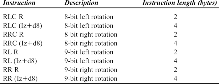
In 8085 the rotate operations are possible only on A register contents. In Z-80 the rotate operations could be performed on the contents of
- any general purpose 8-bit register or memory location pointed by HL;
- memory location whose address is provided using indexed addressing.
These new rotate instructions of Z-80 are shown in Table 27.5. The following convention is used in this table.
R = A, B, C, D, E, H, L, or (HL);
Iz = IX or IY;
d8 = 8-bit unsigned displacement.
Table 27.5 Pure Z-80 Rotate Instructions
RLD and RRD Instructions: In addition to the powerful rotate instructions described, there are two more instructions under the rotate group of instructions. They are RLD and RRD.
RLD instruction: RLD stands for ‘rotate left digit’. It is a 2-byte instruction. The first byte indicates that it is a pure Z-80 instruction, and the second byte indicates that it is RLD instruction. It works on the contents of A register and the contents of memory pointed by HL. There are a total of four hex digits in A register and the memory contents pointed by HL. However, rotate left operation is performed only on three hex digits, leaving the MS hex digit in register A unchanged. It is shown diagrammatically in Fig. 27.6.
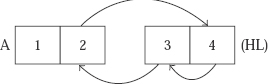
Fig. 27.6 Illustration of RLD instruction
Example:
RRD instruction: RRD stands for ‘rotate right digit’. It is a 2-byte instruction. The first byte indicates that it is a pure Z-80 instruction, and the second one indicates that it is RRD instruction. It works on the contents of Aregister andthe contents of memory pointed by HL. There are a total of four hex digits in Aregister and the memory contents pointed by HL. However, rotate right operation is performed only on three hex digits, leaving the MS hex digit in A register unchanged. It is shown diagrammaticallyin Fig. 27.7.
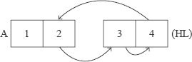
Fig. 27.7 Illustration of RRD instruction
Example:
Shift instructions: Intel 8085 did not have shift instructions. These are the additions in Z-80. A shift instruction just shifts the number in a register or a memory location to the left or to the right by one bit position. There will not be any rotation of the bits in this case. In Z-80 the shift operations could be performed on the contents of
- any general purpose 8-bit register or memory location pointed by HL;
- memory location whose address is provided using indexed addressing.
The shift instructions are of two types: arithmetic shift and logical shift.
Arithmetic Shift Instructions: Arithmetic shift instructions are used when the number to be shifted is interpreted by the programmer to be a signed number. In arithmetic shift operation the sign of the number remains unchanged after the operation.
SRA instruction: SRA stands for ‘shift right arithmetic’. It shifts all the bits to the right by one position. The LS bit that comes out is moved to Cy flag. In the vacancy created at the MS bit position, the earlier MS bit value is retained. The effect of the execution of SRA instruction is indicated in Fig. 27.8.
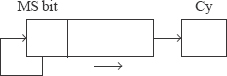
Fig. 27.8 Effect of execution of SRA instruction
A right shift operation divides the signed number by 2, if it is an even number. When an odd number is right shifted, the result is truncated to the nearest integer. For example, when SRA instruction operates on number 5, the result will be 2. Similarly, when SRA instruction operates on number FBH (interpreted as –5), the result will be FDH (interpreted as –3).
The two general formats for the SRA instructions are:
- SRA R of size 2 bytes;
- SRA (Iz+d8) of size 4 bytes
where
R = A, B, C, D, E, H, L, or (HL)
Iz = IX or IY
d8 = 8-bit unsigned displacement.
SLA instruction: SLA stands for ‘shift left arithmetic’. It shifts all the bits to the left by one position. The MS bit that comes out is moved to Cy flag. In the vacancy created at the LS bit position, a 0 value is moved. The effect of the execution of SLA instruction is indicated in Fig. 27.9.
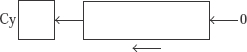
Fig. 27.9 Effect of execution of SLA instruction
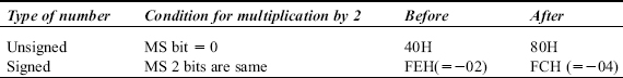
The left shift operation has the same effect immaterial of the number to be shifted being treated as signed or unsigned. The condition for correct multiplication by 2 depends on whether the number before shift is treated as unsigned or signed, as shown in the following table with an example each.
The two general formats for the SLA instructions are:
- SLA R of size 2 bytes;
- SLA (Iz+d8) of size 4 bytes.
Logical Shift Instructions: Logical shift instructions are used when the number to be shifted is interpreted by the programmer to be an unsigned number.
SRL instruction: SRL stands for ‘shift right logical’. It shifts all the bits to the right by one position. The LS bit that comes out is moved to Cy flag. A 0 value is movedin the vacancy created at the MS bit position. The effect of the execution of SRL instruction is indicated in Fig. 27.10.
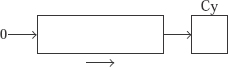
Fig. 27.10 Effect of the execution of SRL instruction
A right shift operation divides the signed number by 2, if it is an even number. When an odd number is right shifted the result is truncated to the nearest integer. For example, when SRL instruction operates on number 5, the result will be 2. Similarly, when SRL instruction operates on number FBH, the result will be 7DH.
The two general formats for the SRL instructions are:
- SRL R of size 2 bytes;
- SRL (Iz+d8) of size 4 bytes.
Similarly, the ‘shift left logical’ instruction shifts all the bits to the left by one position. The MS bit that comes out is moved to Cy flag. A 0 value is moved in the vacancy created at the LS bit position. This same action is performed when SLAinstruction is executed. As such, there is no ‘shift left logical’instruction in the instruction set of Z-80. Whenever ‘shift left logical’ operation is desired, an SLA instruction isexecuted.
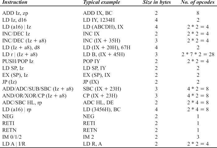
Other Instructions: The remaining pure Z-80 instructions are provided in Table 27.6. The following convention is used in describing the instructions.
Iz = IX or IY;
zp = BC, DE, Iz, or SP (note that HL is not allowed);
d16 = 16-bit immediate data;
a16 = 16-bit address;
a8 = 8-bit address;
r = A, B, C, D, E, H, or L;
rp = BC, DE, HL, or SP.
INC/DEC Iz stands for INC Iz and DEC Iz;
LD Iz | (a16) stands for LD Iz, (a16) and LD (a16), Iz;
IM 0/1/2 stands for IM 0, IM 1, and IM 2.
Table 27.6 Pure Z-80 Instructions with Examples
27.6 PINS OF Z-80
The devices normally used along with Z-80 to provide the required functions in a microcomputer are: Z-80 PIO (similar to 8255 PPI) and Z-80 CTC (similar to 8253 timer).
The actual pin diagram and the functional pin diagram of Z-80 are provided in Figs. 27.11 and 27.12, respectively.
Fig. 27.11 Pin diagram of Z-80
Fig. 27.12 Functional pin diagram of Z-80
The Z-80 is probably the only 8-bit microprocessor to provide refresh facility on chip for DRAMs. However, it is not normally made use of. This is because of the fact that, SRAMs are used mostly in Z-80-based systems, as the maximum memory addressing capacity is a meager 64K bytes.
27.7 INTERRUPT STRUCTURE IN Z-80
The Z-80 has two external interrupt pins, which are NMI* and INT*. Although there are only two interrupt pins, compared with the five in 8085, the Z-80 has a superior interrupt structure than the 8085.
27.7.1 INT* INTERRUPT
INT* is an active low, level-triggered interrupt input pin. This is an interrupt that could be masked or disabled. The execution of DI instruction disables this interrupt. In such a case, even if an I/O port activates the INT* pin, the Z-80 will not be interrupted. Even after a reset of Z-80 the INT* interrupt is disabled. The Z-80 is always started with activation of reset. Thus, in a Z-80 program, if it is desired that the Z-80 should be interrupted by INT* pin, then the EI instruction must be present in the program. The INT* interrupt is enabled only after the execution of the EI instruction.
The action performed by the Z-80 when INT* pin is activated depends on the interrupt mode of Z-80. There are three interrupt modes that are: interrupt mode 0, interrupt mode 1, and interrupt mode 2.
Interrupt mode 0 (IM 0): This is actually a 2-byte instruction of Z-80 with the opcode ED 46H. After the execution of this instruction the INT* input of Z-80 works in IM 0. In fact, this is the default mode of operation after reset of Z-80. Thus if the interrupt mode type is not explicitly specified by executing one of IM 0, IM 1, or IM 2 instructions, the Z-80 works in IM 0.
INT* in IM 0 mode of operation is very similar to INTR interrupt of 8085. INT* in IM 0 mode of operation acts like a non-vectored interrupt. In this mode the Z-80 will respond to the interrupt request by activating IORQ* and M1* signals. The simultaneous activation of IORQ* and M1* is the Z-80 way of informing the peripherals that it is issuing an interrupt acknowledgement. The Z-80 expects the interrupting peripheral to respond (as IORQ* = 0) with an opcode byte (as M1* = 0). The peripheral should send to the Z-80 an RST instruction or a 3-byte CALL instruction using the data lines of Z-80. The Z-80 will automatically disable the interrupt system. The user is not required to explicitly use DI instruction. The Z-80 will save the address of the next instruction (same as PC contents) above the stack top. Then the Z-80 branches to the ISS indicated by the peripheral using RST or CALL instruction.
Thus the action taken by Z-80 when interrupted half way through an instruction because of INT* in IM 0 mode could be summarized as follows. It is assumed that NMI* is not active and the interrupt system is enabled using EI instruction.
- Completes the execution of the instruction under progress.
- Activates IORQ* and M1*.
- Receives an RST or a CALL instruction from the peripheral.
- Disables the interrupt system.
- Saves PC value (address of next instruction) on the stack top.
- Branches to the ISS indicated by the peripheral.
The format of the INT* service routine will generally be as follows.
- Save all the registers.
- Perform the action needed to satisfy the interrupting device.
- Restore all the register contents.
- Enable the interrupt system using EI instruction.
- Return to main program by executing RETI instruction.
RETI stands for ‘RETurn from INT serviceroutine’. It is a 2-byte instruction with the code ED 4DH. The RETI instruction pops the return address from the stack top to PC. This ensures return to main program. The Z-80 peripheral chips recognize this instruction and understand that the interrupt service is over. In other respects, RETI is the same as RET instruction.
The following instructions perform the saving of all the general-purpose 8-bit registers and the flags register in the alternate set of registers using only 4 + 4 = 8 clock cycles.
EXX
EX AF, AF′
This is much faster than using the following instructions that would take up 4 * 11 = 44 clock cycles. In an 8085-based system, the registers had to be saved on the stack only.
PUSH AF
PUSH BC
PUSH DE
PUSH HL
Executing the following instructions would perform restoring of all the general-purpose 8-bit registers and the flags register from the alternate set of registers using only 4 + 4 = 8 clock cycles.
EXX
EX AF, AF′
This is much faster than using the following instructions that would take up 4 * 10 = 40 clock cycles. Thus the interrupt response is much faster in Z-80 compared with 8085.
POP HL
POP DE
POP BC
POP AF
Thus the general format of an INT* ISS will be as shown in Fig. 27.13. In case index registers are to be used in the service routine, they also have to be saved and restored using PUSHIz and POP Iz instructions in the service routine.
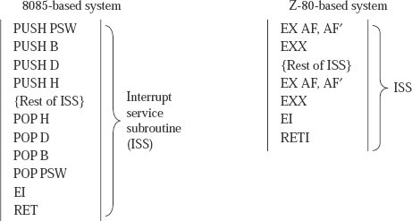
Fig. 27.13 General format for INT* service routine
Interrupt mode 1 (IM 1): This is actually a 2-byte instruction of Z-80 with the opcode ED 56H. After the execution of this instruction the INT* input of Z-80 works in interrupt mode 1.INT* in IM 1 mode of operation is very similar to RST 5.5, RST 6.5, or RST 7.5 which are the vectored interrupts of 8085.
The Z-80 knows the location to branch in this case that is understood to be 0038H. Hence there is no activation of IORQ* and M1* in IM 1 mode.
The Z-80 will automatically disable the interrupt system. The user is not required to explicitly use DI instruction. The Z-80 will save the address of the next instruction (same as PC contents) above the stack top. The Z-80 then branches to the ISS at the specific location 0038H. Hence the action taken by Z-80 when interrupted half way through an instruction because of INT* in IM 1 mode could be summarized as follows. It is assumed that NMI* is not active and interrupt system was enabled using EI instruction.
- Completes the execution of the instruction under progress.
- Disables the interrupt system.
- Saves PC value (address of next instruction) on the stack top.
- Branches to the ISS at 0038H.
In Z-80 kit, there could be an unconditional jump to a system RAM location as part of the monitor program at location 0038H. For example, the instruction ‘JP 8FF3H’ could be present in the three locations starting from 0038H. Again at location 8FF3H there could be an unconditional jump to a user RAM location as part of the user program. For example, the instruction ‘JP 9C00H’ could be present in the three locations starting from 8FF3H. In such a case, the INT* service routine in IM 1 mode starts fromlocation 9C00H, as indicated in Fig. 27.14.
Fig. 27.14 Branching to service routine in IM 1 mode
This mode is functionally the same as IM 0 mode if the peripheral sends RST 38H instruction or CALL 0038H instruction. The advantage of IM 1 mode is that no external hardware is neededto supply the service routine address. It is useful in applications that have a single interrupt source. The disadvantage is that if several interrupt sources are present, there is no direct way in this modeto identify the source of interrupt.
Interrupt mode 2 (IM 2)M: This is actually a 2-byte instruction of Z-80 with the opcode ED 5EH. After the execution of this instruction the INT* input of Z-80 works in interruptmode 2. INT* in IM 2 mode of operation has no parallel in 8085. The advantage of IM 2 mode is that as many as 128 interrupting sources could be present in the system. Each interrupting source sends a unique 8-bit address to the Z-80 in response to simultaneous activation of IORQ* and M1*. Based on the 8-bit address received the Z-80 branches to one of the 128 possible service routines. It is a very powerful mode indeed.
The IM 2 mode resembles both IM 0 and IM 1 modes to some extent. The response of Z-80 for activation of INT* in IM 2 mode is explained with an example
If INT* is activated when Z-80 is in IM 2 mode, then the Z-80 will complete the execution of the instruction in progress. The Z-80 will then respond to the interrupt request by activating IORQ* and M1* signals. The Z-80 expects the interrupting peripheral to respond with an 8-bit address. Hence, the peripheral should send an 8-bit address to the Z-80 using the data lines of Z-80. Let us say 09H =00001001 is received by the Z-80. The Z-80 always treats the LS bit of this address as 0 immaterial of what is received. Thus, the 8-bit address received is treated as 00001000=08H. This is interpreted as the LS byte of a 16-bit address pointer. The MS byte of this 16-bit address pointer is understood to be provided by I register contents. I register stands for ‘interrupt vector register’ which is loaded using the instruction ‘LD I, A’. If the I register content is 05H, then 0508H is taken as a16-bit address pointer. If I register contains 05H, the Z-80 treats memory locations 0500H to 05FFH to provide an interrupt vector table. In this table, which contains 256 memory locations, 128 ISS addresses, each of 2 bytes, are stored. Assume that in locations 0508H and 0509Hthe bytes 12H and 34H, respectively are stored as shown in Fig. 27.15. In such a case, the Z-80 branches to the service routine at location 3412H. In this manner, the Z-80 can branch to any one of the 128 interrupt service routines based on the 8-bit address pointer it receivesfrom the peripheral.
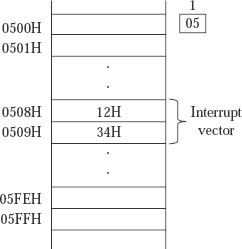
Fig. 27.15 Interrupt vector table in IM 2 mode
Thus, the action taken by Z-80 when interrupted half way through an instruction because of INT* in IM 2 mode could be summarized as follows. It is assumed that NMI* is not active and the interrupt system is enabled using EI instruction.
- Completes the execution of the instruction under progress.
- Activates IORQ* and M1*.
- Receives an 8-bit address pointer from the peripheral.
- Treats this as LS byte of address pointer after making LS bit as 0.
- Contents of I register is treated as MS byte of address pointer.
- Disables the interrupt system.
- Saves PC value (address of next instruction) on the stack top.
- Branches to the ISS pointed by the address pointer.
27.7.2 NMI* INTERRUPT
The NMI* is negative edge triggered interrupt input. It has higher priority over INT*. Also, whenever the NMI* pin is activated, the Z-80 always responds by executing the appropriate ISS. In other words,this interrupt is non maskable. It is a vectored interrupt, very similar to the TRAP interrupt input of 8085. It always branches to the service routine at location 0066H. NMI* interrupt is normally used for high priority events such as power failure, and real time clock. After return from the NMI serviceroutine the interrupt system will be restored to the earlier enabled or disabled status.
The action performed by Z-80 when interrupted half way through an instruction because of NMI* could be summarized as follows.
- Completes the execution of the instruction under progress.
- Disables the interrupt system.
- Saves PC value (address of next instruction) on the stack top.
- Branches to the ISS at location 0066H.
In Z-80 kit, at location 0066H there could be an unconditional jump to a system RAM location as part of the monitorprogram. For example, the instruction ‘JP 8FF0H’ could bepresent in the three locations starting from 0066H. Again at location8FF0H there could be an unconditional jump to a user RAM location as part of the user program. For example, the instruction ‘JP 8C00H’ could be present in the three locations starting from 8FF0H. In such a case, the NMI* service routine starts from location 8C00H.
The format of the NMI* service routine will generally be as follows.
- Save all the registers above the stack top.
- Perform the action needed to satisfy the interrupting device.
- Restore all the register contents from the stack top.
- Return to main program by executing RETN instruction.
RETN stands for ‘RETurn from NMI service routine’. The RETN instruction does the following.
- Pop from the stack top to PC. This ensures return to main program.
- Get back to old value of interrupt enable/disable status.
Executing the following instructions could perform the saving of all the registers. It is to be noted that the registers are being saved on the stack instead of alternate registers. This is because, the NMI* can get activated when the Z-80 is half way through INT* service routine. In such a case, the Z-80 should return from NMI* service routine to INT* service routine with the contents ofmain and alternate set of registers unchanged.
PUSH AF
PUSH BC
PUSH DE
PUSH HL
PUSH IX
PUSH IY
EX AF, AF′
EXX
PUSH AF
PUSH BC
PUSH DE
PUSH HL
Executing the following instructions would perform restoring of all the registers by popping in reverse order.
POP HL
POP DE
POP BC
POP AF
EX AF, AF′
EXX
POP IY
POP IX
POP HL
POP DE
POP BC
POP AF
27.8 PROGRAMMING EXAMPLES
27.8.1 ADDITION OF MULTI-BYTE NUMBERS
Write an Z-80 assembly language program to add two multi-byte numbers. The size in bytes of the two multi-byte numbers is provided in location 8910H. The first multi-byte number starts from location 8920H and the second one from location 8940H. The result is to be stored from location 8970H. For the result, one extra location is provided to account for the carry generated.
A typical input and the expected output are indicated in Fig. 27.16.
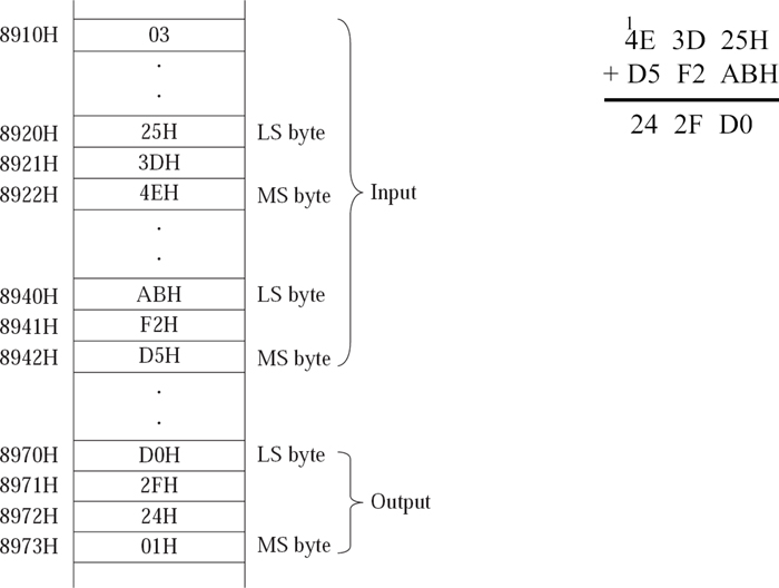
Fig. 27.16 Addition of two multibyte numbers
SCF
        CCF

        LD HL, 8910H
        LD IX, 8920H

AGAIN:  LD A, (IX + 0)
        ADC A, (IX + 20H)
        LD (IX + 50H), A

        INC IX
        DEC (HL)
        JP NZ AGAIN

        JP NC EXIT
        LD (IX + 50H), 01
        HALT

EXIT:   LD (IX + 50H), 00
        HALT
The reader is urged to compare this program with the one in Sect. 15.2 that used 8085 processor. A shortage of registers was felt while using the 8085 processor. The usage of indexed addressing in Z-80 has resulted in a more compact program, and a number of registers of Z-80 are still available for use. This amply demonstrates the power of indexed addressing mode.
27.8.2 EXCHANGE OF BLOCKS
Write an Z-80 assembly language program to exchange the contents of two blocks in memory. The number of elements in the block is provided in location 8910H. The two blocks start at locations 8920H and 8940H, respectively.
A typical input and the expected output are indicated in Fig. 27.17.
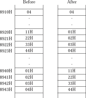
LD HL, 8910H
        LD IX, 8920H

AGAIN:  LD A, (IX + 0)
        LD B, (IX + 20H)

        LD (IX + 00H), B
        LD (IX + 20H), A

       INC IX
       DEC (HL)
       JP NZ AGAIN

       HALT
The reader is urged to compare this program with the one in Sect. 15.1 that used 8085 processor. The usage of indexed addressing in Z-80 has resulted in a more compact program, once again demonstrating the power of indexed addressing mode.
27.8.3 BLOCK MOVEMENT WITHOUT OVERLAP
Write an Z-80 assembly language program to perform block movement. The blocks are assumed to be non overlapping. The block starting at location 8920H is to be moved to that starting at location 8940H. The block size is provided in location 8910H.
A typical input and the expected output are indicated in Fig. 27.18.
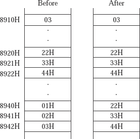
Program
The reader is urged to compare this program with the one in Sect. 15.4 that used 8085 processor. Once again, the useof indexed addressing in Z-80 has resulted in a more compact program.
27.9 INSTRUCTION SET SUMMARY
The Z-80 instruction set summary is provided in Table 27.7. The convention used in this table is as follows.
Table 27.7 The Z-80 Instruction Set Summary
| Mnemonic | No. of opcodes |
| ADD A/ADC A/SUB/SBC A/AND/OR/XOR/CP r/(HL)/(Iz+a8)/d8 | 8 * (7 + 1 + 2 + 1) + 88 |
| INC/DEC r/(HL)/Rp/(Iz+a8) | 2 * (7 + 1 + 6 + 2) =32 |
| ADD/ADC/SBC HL, rp | 3 * 4 = 12 |
| ADD Iz, zp | 2 * 4 = 8 |
| DAA | 1 |
| LD Rp, d16 | 6 |
| LD r1, r2 | 7 * 7 = 49 |
| LD r | (HL) | 7 * 2 = 14 |
| LD r/(HL)/(Iz+a8), d8 | 7 +1 +2 = 10 |
| LD (BC)/(DE)/I/R | A | 4 * 2 = 8 |
| LD A | (a16) | 2 |
| LD r | (Iz+a8) | 7 * 2 * 2 = 28 |
| LD Rp | (a16) | 6 * 2 = 12 |
| LD HL | (a16) | 1 * 2 = 2 |
| LD SP, HL/IX/IY | 3 |
| EX DE, HL; EXX; EX AF, AF′; | 3 |
| EX (SP), HL/IX/IY | 3 |
| IN A, (a8); OUT (a8), A; | 2 |
| IN r, (C); OUT (C), r; | 7 + 7 = 14 |
| INI/INIR/INI/INDR/OUTI/OTIR/OUTD/OTDR | 8 |
| LDI/LDIR/LDD/LDDR | 4 |
| CPI/CPIR/CPD/CPDR | 4 |
| BIT/SET/RESn, r/(HL)/(Iz+a8) | 3 * 8 * (7 +1 +2) = 240 |
| RLC/RRC/RL/RR/SLA/SRA/SRL r/(HL)/(Iz+a8) | 7 * (7 +1 +2) = 70 |
| RLCA/RRCA/RLA/RRA | 4 |
| RLD/RRD | 2 |
| CALL/JP a16 | 2 |
| CALL/JP cond, a16 | 2 * 8 = 16 |
| JP (HL)/(IX)/(IY) | 3 |
| DJNZ/JR r8 | 2 |
| JR C/NC/Z/NZ r8 | 4 |
| RET cond | 8 |
| RET/RETI/RETN | 3 |
| RST 0/ 8/ 10H/ 18H/ 20H/ 28H/ 30H/ 38H | 8 |
| IM 0/1/2 | 3 |
| PUSH/POP BC/DE/HL/AF/IX/IY | 2 * 6 = 12 |
| CPL/NEG/CCF/SCF/HALT/NOP/EI/DI | 8 |
a16 = 16-bit address;
a8 = 8-bit address;
r8 = 8-bit signed displacement.;
r, r1, r2 = A, B, C, D, E, H, or L;;
Iz = IX or IY;;
rp = BC, DE, HL, or SP;;
Rp = BC, DE, HL, SP, IX, or IY;;
zp = BC, DE, Iz, SP;
that is, if Iz = IX then zp = BC, DE, IX, SP and if Iz = IY then zp = BC, DE, IY, SP;;
n = 0, 1, 2, ..., 7;;
cond = C/NC/Z/NZ/P/M/PO/PE.
- Explain the improvements in 8085 over 8080.
- Provide a brief description of the programmer's view of Z-80.
- Explain the flags of Z-80.
- Explain relative addressing in Z-80 and its advantages. List the various conditional relative jump instructions of Z-80.
- Explain indexed addressing mode of Z-80 with an example.
- Write the mnemonic in Z-80 for the instructions whose purpose is indicated as follows. Also indicate the instruction size in each case.
- Instruction to set bit 5 of D register.
- Instruction to reset bit 6 of memory location pointed by HL.
- Instruction to test bit 7 for a zero value of memory location 4560H, when IX register is 4500H, using indexed addressing.
- Write a short note on the opcode size of Z-80 instructions.
- Explain the difference in the functioning of DAA instruction in 8085 and Z-80.
- Write a note on the I/O instructions in Z-80.
- Explain the shift instructions available in Z-80 with examples.
- With a neat functional pin diagram explain the pins of Z-80.
- Explain the response by Z-80 when NMI* interrupt is activated.
- Explain the various modes of operation of INT* in Z-80.
- Explain the following instructions of Z-80 with examples.
- EXX
- EX AF, AF′
- DJNZ BACK
- LDIR
- LDD
- CPDR
- INIR
- IND
- OTDR
- OUTI
- RLD
- RRD