Getting Started
Abstract
For those of you who are familiar in setting up projects and drawing schematics in Capture, you may want to skip this chapter as this chapter is for those of you who have little or no experience of using Capture. The chapter will describe how to start Capture and how to set up the project type and libraries for PSpice simulation. The chapter will also introduce some of the features found in the latest software releases. At the end of each chapter there are some exercises to do and as you go through the book, each chapter will build upon the exercises from previous chapters.
Keywords
Simulation; Components; Resistor; Voltage; Circuits
For those of you who are familiar in setting up projects and drawing schematics in Capture, you may want to skip this chapter as this chapter is for those of you who have little or no experience of using Capture. The chapter will describe how to start Capture and how to set up the project type and libraries for PSpice simulation. The chapter will also introduce some of the features found in the latest software releases. At the end of each chapter there are some exercises to do and as you go through the book, each chapter will build upon the exercises from previous chapters.
1.1 Starting Capture
Circuit diagrams for PSpice simulation are drawn in either Capture or Capture component information system (CIS) schematic editor. The CIS option allows you to select and place components from a component database instead of selecting and placing components from a library. For this book, it does not matter if the circuits are drawn in Capture or Capture CIS.
If you have the software installed under the OrCAD name, launch Capture or Capture CIS, by clicking on:
Start > Program Files > OrCAD xx.x > Capture
or
Start > Program Files > OrCAD xx.x > Capture CIS
where xx.x is the version number, i.e., 10.5, 11.0, 15.5, 15.7, 16.0, 16.2, 16.3, 16.5, or 16.6.
For example:
Start > All Programs > Cadence > OrCAD 16.6 Lite > OrCAD Capture CIS Lite
Start > All Programs > Cadence > Release 16.5 > Capture
If you have the Cadence software installed, the products are installed under the Allegro platform name. In this case, only Capture CIS is available and is branded as Design Entry CIS.
Start > Program Files > Allegro SPB 16.6 > Design Entry CIS
For the 17.2 release:
Start > All Programs > Cadence Release 17.2-2016 > OrCAD Lite Products > Capture CIS Lite
or
Start > All Programs > Cadence Release 17.2-2016 > OrCAD Products > Capture
1.2 Creating a PSpice Project
New designs started in Capture will automatically create a project file (.opj) that references the design file (.dsn) and associated project files such as the libraries and output report files. The design file encapsulates the schematic folders and associated schematic pages. For example, you may want to have separate schematics for each stage of your design rather than have one complete circuit. An advantage of this hierarchical design approach provides selective simulation of individual circuits. Alternatively, you can have a flat design where more than one page is associated with just one schematic folder. Either way, one schematic folder known as the root folder, signified by a “/” and one associated page will be created initially for the project. Other schematic folders and pages can be added at a later stage.
Before the circuit diagram is drawn, the project type and libraries attached to the project need to be set up. This can be done by clicking on the New Project icon on the Start Page under the Getting Started heading. For previous software releases, select from the top tool bar, File > New > Project.
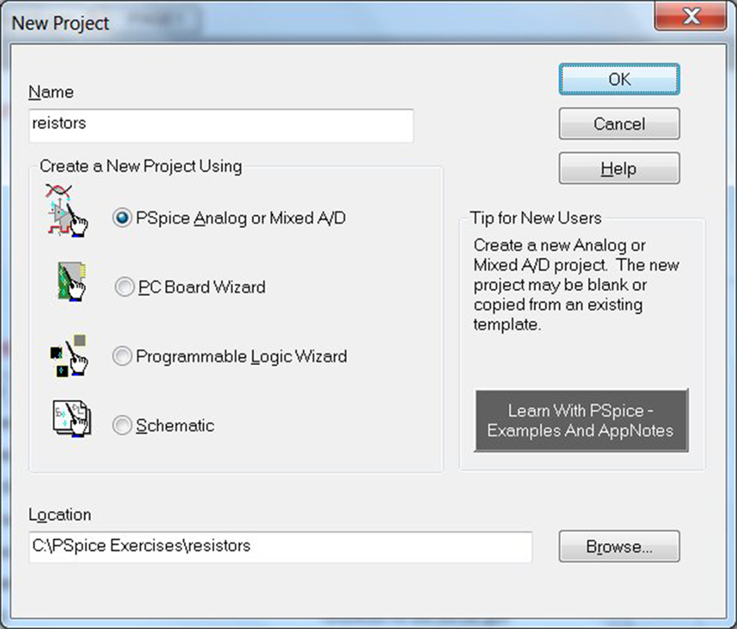
In the New Project window (Fig. 1.1) you enter the name of the project and then you have a choice of one of four project types.

• Analog or Mixed A/D is used for PSpice simulations.
• PC Board Wizard is used for schematic to PCB projects.
• Programmable Logic Wizard is used for CPLD and FPGA designs.
• Schematic is used for schematic and wiring diagrams.
When you select a Project type, the Tip for New Users gives a brief explanation of the project type. For PSpice projects, select Analog or Mixed A/D. This will activate the PSpice menu on the top toolbar in Capture. In release 17.2, the New Project Dialog Box incorporates the Learn with PSpice link that provides access to Examples and AppNotes.
It is recommended that a new directory location (folder) should be created for each new project. This can be done by clicking on the Browse button in Fig. 1.1 that opens up Windows Explorer allowing you to create and name the project folder. If you have a previous software release to 17.2, then when you click on the Browse button in Fig. 1.1, the Select Directory window appears as shown in Fig. 1.2.
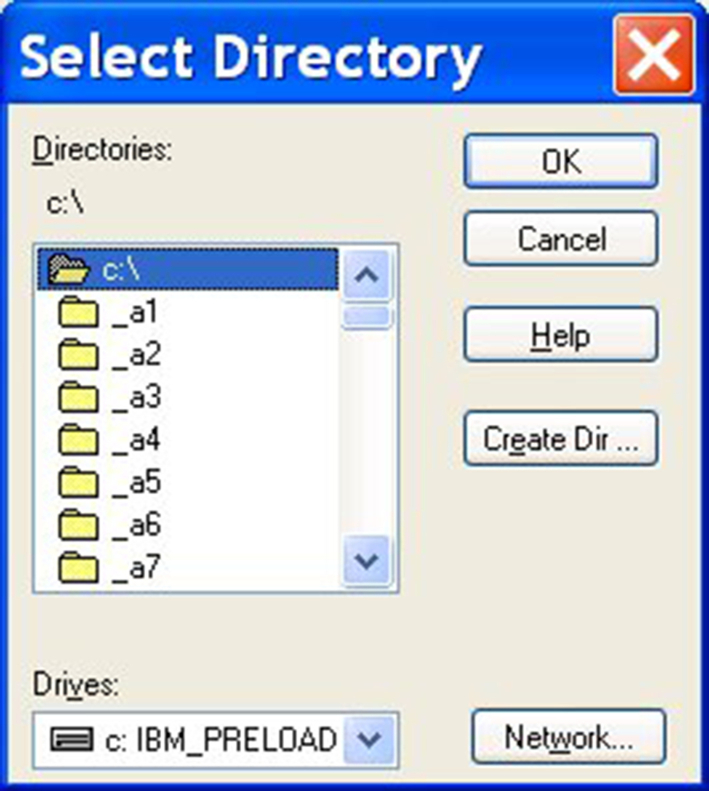
By selecting the Create Dir… button, the Create Directory window (Fig. 1.3) appears that allows you to name the directory (folder).

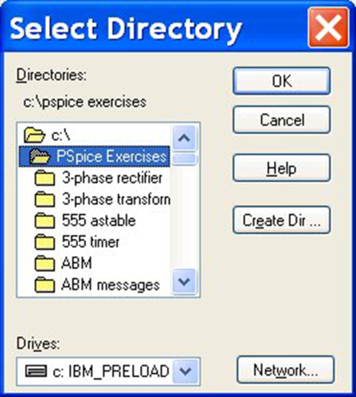
The newly created folder, PSpice Exercises, in this example, will appear in the Select Directory window. However, you must highlight the folder and click OK in order to ensure that the folder is active. The folder will then appear as an “open” yellow folder as shown in Fig. 1.4. This allows you the option to add further subfolders by clicking on Create Dir and following the same procedure as above. If no folders are to be added, then just click on OK.
The project folder location will then appear in the Location box of the Project Manager (see Fig. 1.1). See exercises at the end of the chapter.
An alternative method of creating the project folder is to type in the folder location path directly into the Location box in the Project manager in Fig. 1.1 and Capture will automatically create the folder.
The next dialog box to appear is the Create PSpice Project window which sets up the project for PSpice simulation (Fig. 1.5).

The pull down menu option allows you to select preconfigured Capture-PSpice.
The pull down menu option allows you to select preconfigured Capture-PSpice projects and a selection of configured libraries. In previous Lite versions, a default eval.olb library was available for projects. Now all PSpice libraries are included with the Lite version.
There is also an option to create updated versions of an existing project, i.e., to create a newer version 2 based upon the original version 1 project. You select the function, Create based upon an existing project and then Browse to select an existing project which will copy the project and all its associated files into the new project. This is similar to using the File > Save As function from the File menu.
If the Create a blank project option is selected, then no Capture-PSpice libraries are added to the project. The libraries can be added later. This will be demonstrated in one of the exercises at the end of this chapter.
When a new project is created, a Project Manager window is created as shown in Fig. 1.6. In this example, the simple library option consisting of 5 default libraries has been selected. In this example, the resistors.dsn file has been expanded to show the SCHEMATIC1 folder and the underlying PAGE1 in which you draw the circuit diagram.
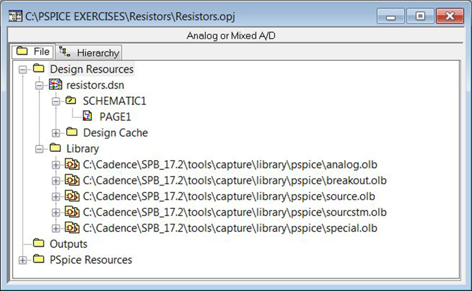
The Project Manager also shows the absolute path to the libraries. Remember that these are Capture parts libraries which define the graphics for the parts. They are not the PSpice model libraries. The preinstalled Capture libraries can be found, depending on the OrCAD or Cadence software version you are using, for example:
< software install path > OrCad > OrCAD_16.6_Lite > tools > capture > library > pspice
or
< software install path > Cadence > SPB_16.6 > tools > capture > library > pspice
Normally the < software install path > is on the C: drive, for example:
C:CadenceSPB_17.2 oolscapturelibrarypspice
Tip
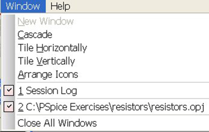
If the Project Manager window is not displayed, select from the top tool bar, Window > < project name >.opj file as shown in Fig. 1.7. Here the project name is resistors. Note the project name file extension .opj.
Alternatively, click on either of the Project manager icons. 

1.3 Symbols and Parts
Before drawing a schematic diagram, it is useful to know the difference between a part and a symbol.
Parts are graphical objects where the part name represents for example a 2N3906 transistor, an LF411 opamp, etc. Connecting wires drawn to Capture parts are known as nets and they have net names known as a net alias. Capture will assign a default net alias to a wire but the default name can be changed. It is always good practice to rename default nets to more meaningful names such as out, clock, + 5 V, etc.
Symbols are also graphical parts but the wires connected to symbols inherit the name of the symbol. For example, when placing a “0” symbol to represent a ground connection, the connecting wire will take on the net name of “0.” To define a + 5V connection you can use a generic VCC_CIRCLE symbol and rename it to + 5 V. All wires connected to the + 5 V symbol will take on a net name of + 5 V. There are many different symbols you can use to define power, ground, and digital logic level connections and you can rename them accordingly.
1.3.1 Symbols
Symbols also differ from parts in that they are not placed from the Place Part menu in Capture. Instead you have to select the symbol from the Place menu. Fig. 1.8 shows the top portion of the Place menu.

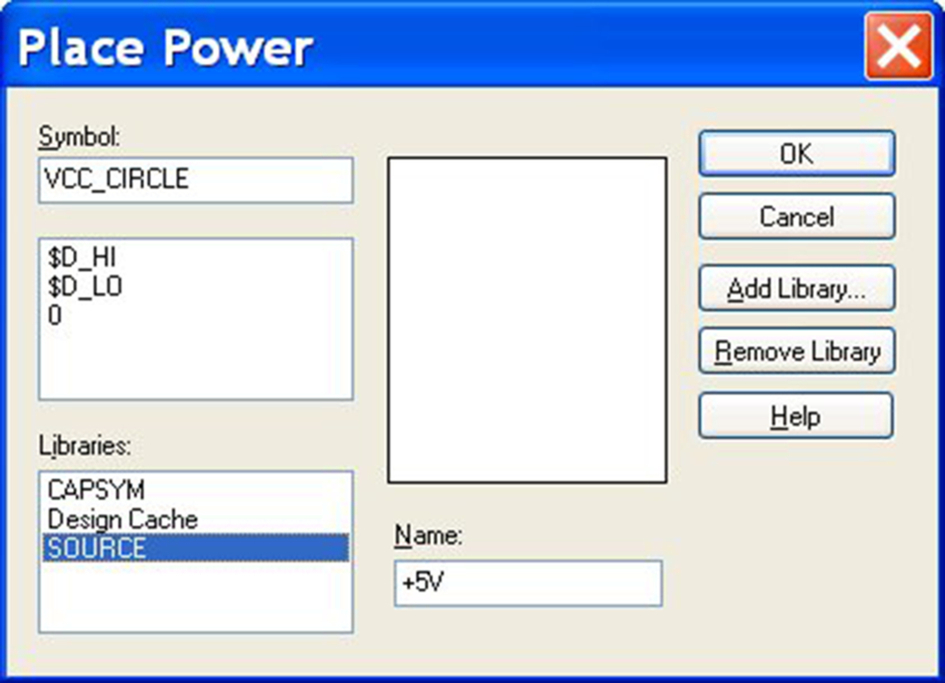
The Place menu also shows the corresponding short cut keys. For example to place a Power symbol, press F and the Place Power menu appears as shown in Fig. 1.9.

In the Place Power menu in Fig. 1.9, a VCC_CIRCLE symbol has been selected and its name has been changed to + 5 V. Any wires (nets) connected to + 5 V will take on the net name + 5 V.
Other symbols include hierarchical ports and off-page connectors which allow signals to be connected together throughout the design. These will be discussed in a later Chapter.
There are two symbol libraries, source and capsym. Capsym contains all the analog ground and power symbols. The source library also contains the analog 0V symbol and also the digital $D_HI and $D_LO symbols that are used to set a digital level of “HI” or “LO” on a wire or pin of an IC.
1.3.2 Parts
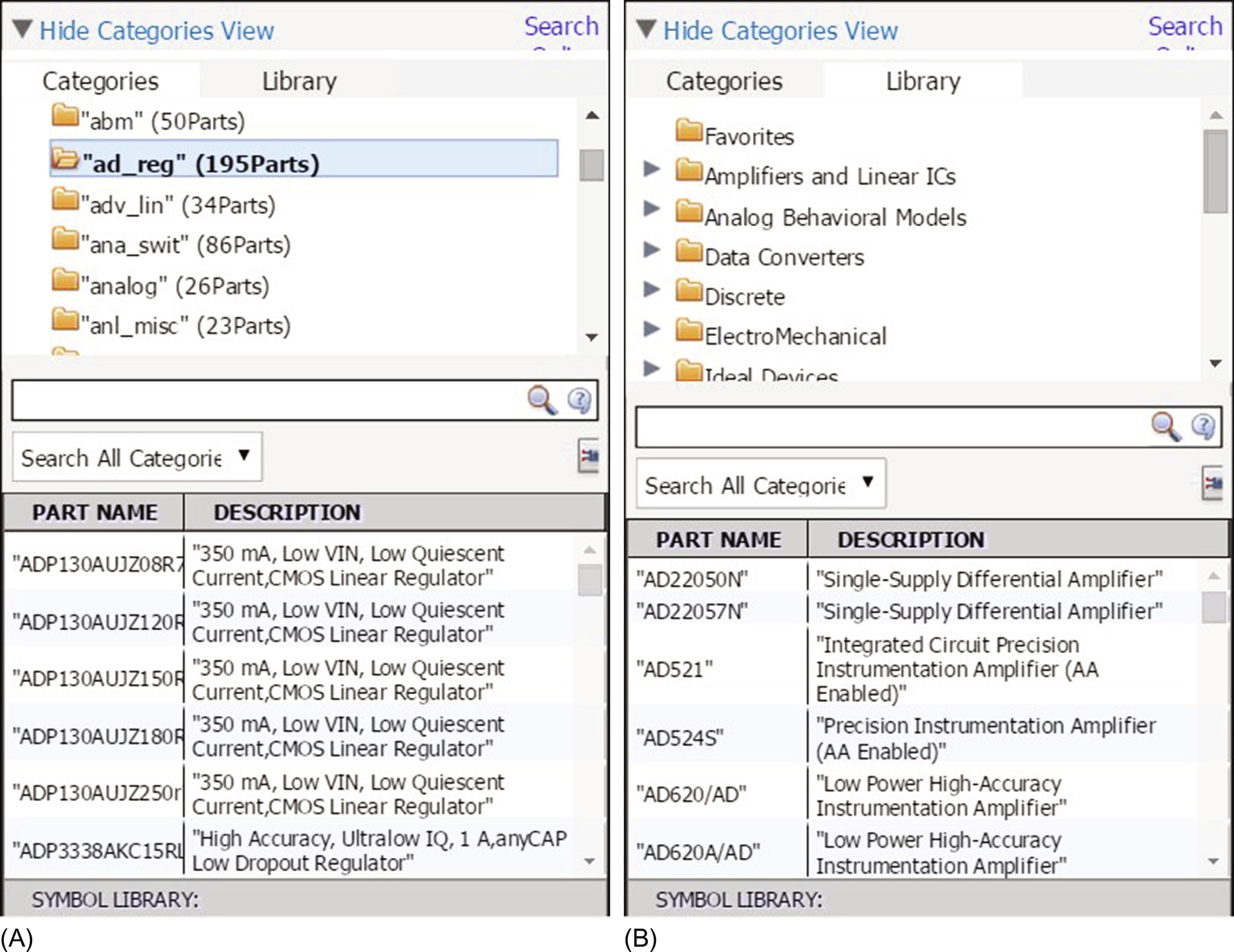
To place a part, select, Place > Part. Fig. 1.10A shows the Place Part window for earlier Capture versions and Fig. 1.10B shows the Place Part window in later versions.

Although the two Place Part windows look different, they have the same functionality in that they display the list of libraries available and the parts available in those libraries. They also provide a part search function. In Fig. 1.10A, only the analog library has been highlighted and so only those parts for that library are shown in the Parts List.
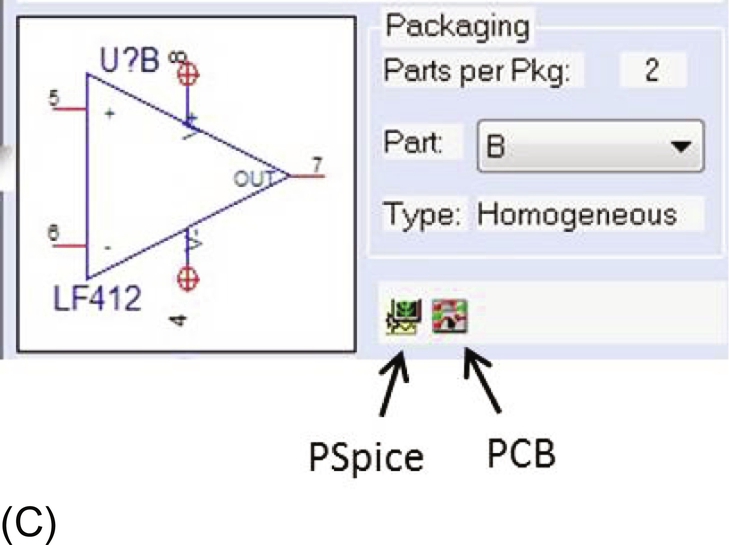
In Fig. 1.10B, all the libraries have been highlighted and so you see the name of the part (LF412) and the library it comes from (OpAmp). If you place the cursor over any part in the Parts List, a tool tip rectangular bar appears giving the absolute path name to the library part. The graphical description for the LF412 shows that there are 2 parts per package and part A has been selected. Selecting B will show a similar part with different pin numbers (see Fig. 1.10C). The part is homogenous in that all parts in the package are the same and have the same number of pins. A solid-state relay with a coil and a switch is an example of a heterogeneous type in which the parts in the package are not the same.
The green PSpice icon indicates that a PSpice model is attached to the LF412 and can therefore be simulated. The red icon indicates a PCB footprint is attached to the part.
In the Place Power or Place Ground window (Fig. 1.11), there is a source library that contains only the digital HI and LO and ground 0V symbols.
To recap, symbols are placed from the Place menu and parts are placed from the Place > Part menu. Also note that both Part libraries and Symbol libraries have an .olb extension and are the Capture graphical parts.
1.3.3 Search for Parts
In the Place Part window dialog box (Fig. 1.10A) there is a Search for Part function that enables you to search for parts in any of the preinstalled and other custom-created libraries. If searching for standard vendor parts, it is recommended that wildcard characters be used as different semiconductor vendors tend to append their own numbers and letters to industry standard part numbers; for example, LF412CN/NOPB, LF412CP, LF412ACN/NOPB, LF412CPE4, LF412CDR, etc. So to search for an LF412 you would use LF412⁎ where “⁎” is a wildcard so any characters or numbers after LF412 are ignored during the search. The “?” character is used to ignore individual characters, for example to look for a logic gate function based on the 7408, irrespective of family type, you could use 74??08. Fig. 1.12 shows the search results for an AD648 of which there are three types, the AD648A, AD648B, and AD648C.

In 17.2 and later versions of 16.6, a database of available PSpice parts has been added that enables you to search for parts not only by name but also by categories. Categories are very useful if you are looking for a specific type of part, i.e., a FET input operational amplifier or a single supply operational amplifier. The PSpice Part Search window shown in Fig. 1.13 is opened by selecting:
Place > PSpice Component > Search
Fig. 1.13A shows the installed libraries that are available and the parts within the libraries. In Fig. 1.13B, the library parts are shown as categories, i.e., Pressure sensors, Operational amplifiers, data converters, etc.
You can search for a part in all categories or just one selected category (see Fig. 1.14). Selecting the Symbol Viewer icon, symbols can be viewed before being placed in the schematic page. The Symbol Viewer updates every time you select a new part. You can only select and place one part at a time.

When you select the Search Online icon, the online search facility opens up the OrCAD Capture Marketplace website that acts as a portal to search vendor websites for Capture parts, IBIS, Verilog, VHDL, and PSpice models.
1.3.4 Quick Place of PSpice Components
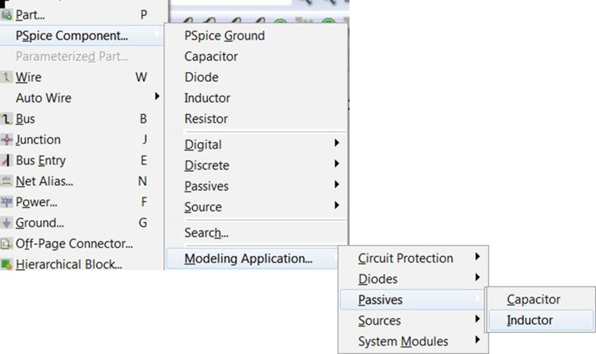
From release 16.6, there is a new feature which allows you to quickly place generic PSpice parts rather than search for vendor-specific semiconductor device numbers. Parts are placed from the top tool bar, Place > PSpice Component menu as shown in Fig. 1.15.

The first five components represent the most common components used in a schematic. The PSpice Ground (Hot key—G) is from the source library and the discrete components are from the analog library. Table 1.1 summarizes the list of available Quick Place PSpice components and their library of origin.
Table 1.1
List of available Quick Place PSpice components
| Components | Capture library | Simulation ready | |
| Digital | |||
| Gates | AND,OR,NAND,NOR,XOR,INV | dig_prim | √ |
| Flip-Flop | D,JK,RS,T | dig_prim | √ |
| ADC | 8 bit, 10 bit, 12 bit | breakout | √ |
| DAC | 8 bit, 10 bit, 12 bit | breakout | √ |
| Discrete | |||
| Diode, NPN, PNP, NPN Darlington, PNP Darlington, NMOS, PMOS, Power NMOS, Power Diode, N-JFET, P_JFET, IGBT, GAsFET | breakout.olb | √ | |
| OpAmp | analog.olb | √ | |
| Passives | |||
| R, C, L, TLine ideal, TLine lossy | analog.olb | √ | |
| Potentiometer, coupling | breakout.olb | √ | |
| Source | |||
| Controlled sources | VCVS, VCCS, CCVS, CCCS | analog.olb | √ |
| Current sources | AC, DC, pulse, sine, exponential, FM sine | source.olb | √ |
| Voltage sources | AC, DC, pulse, sine, exponential, FM sine | source.olb | √ |

Components from the breakout library are generic semiconductor parts with default names and parameters that can be customized using the PSpice Model Editor. In the demo and Lite software versions, only diodes can be edited in the Model Editor. The Model Editor is introduced in a later chapter.
If you know the actual semiconductor device number, then it may be best to find and use that known semiconductor device from the PSpice libraries. The generic parts are useful if you are new to electronics and you just want to get a circuit up and running quickly. Customizing semiconductor parts from the breakout library is mainly used for more advanced circuits where specific semiconductor characteristics are required.
1.4 PSpice Modeling Applications
New PSpice models are normally created in the Model Editor (see Chapter 16). However, from release 16.6, the PSpice Modeling Application provides a quick method to create PSpice models in Capture. The application can be found under the Place menu; Place > PSpice Components > Modeling Applications.
For example, to create a PSpice inductor model, select Passives then Inductors from the pull down menu (see Fig. 1.16).
You can then add the manufacturer's data for the inductor parameters such as tolerance, temperature coefficients, and parasitics as shown in Fig. 1.17.
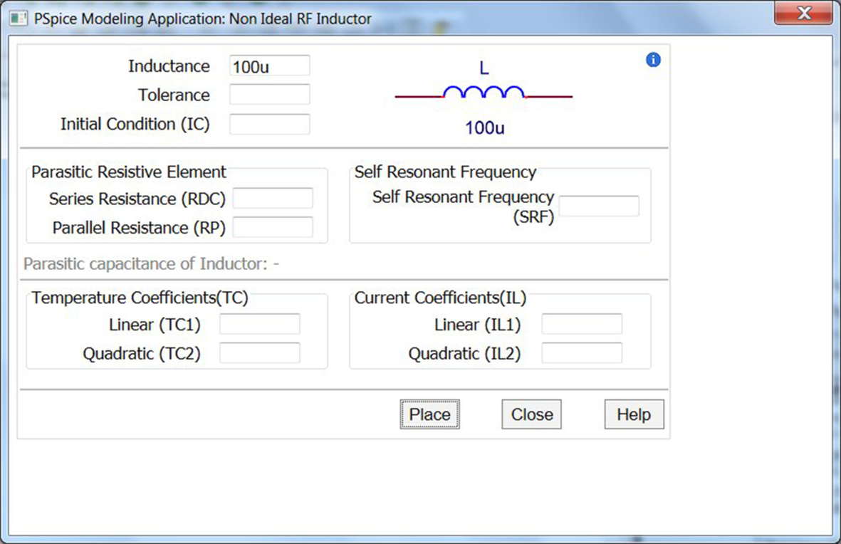
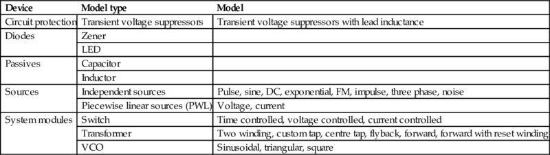
Table 1.2 lists the PSpice components that can be created in Capture using PSpice Modelling Applications.
Table 1.2
Modelling Applications PSpice models
| Device | Model type | Model |
| Circuit protection | Transient voltage suppressors | Transient voltage suppressors with lead inductance |
| Diodes | Zener | |
| LED | ||
| Passives | Capacitor | |
| Inductor | ||
| Sources | Independent sources | Pulse, sine, DC, exponential, FM, impulse, three phase, noise |
| Piecewise linear sources (PWL) | Voltage, current | |
| System modules | Switch | Time controlled, voltage controlled, current controlled |
| Transformer | Two winding, custom tap, centre tap, flyback, forward, forward with reset winding | |
| VCO | Sinusoidal, triangular, square |
1.5 Design Templates
Capture release versions of 16.3 to 16.6, included design templates of complete electronic circuits and topologies including simulation profiles for analog, digital, mixed, and switched mode power supplies. You select any of these design templates from the pull down menu in the Create PSpice Project dialog box when you create a new project see Fig. 1.18.
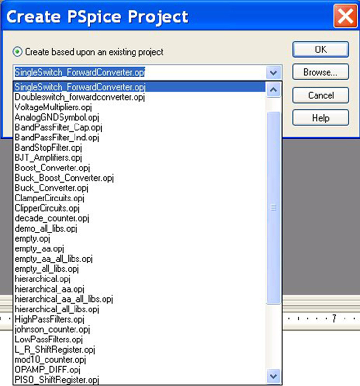
Fig. 1.19 shows the design template for a single switch forward converter which includes the schematic and explanatory text.

1.6 Demo Designs
From release 17.2 onward, the Open Demo Designs window provides access to all types of design examples included with the installed software. Over 150 demo designs can be accessed by; File > Open > Demo Designs (Fig. 1.20).
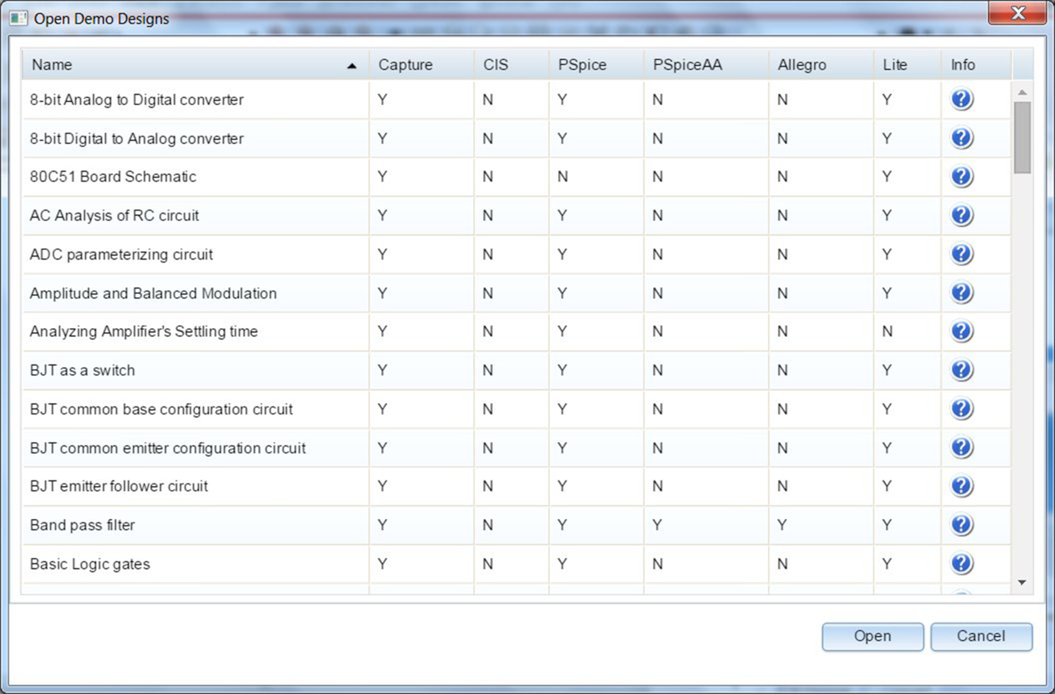
The designs are complete working circuits and include circuit equations and theory.
1.7 Exporting Capture Designs
From the 16.3 version of Capture, the schematic design can be exported to a PDF file with searchable text. This is especially useful when sending designs to those who do not have the OrCAD software installed but have Adobe Reader installed. To export a PDF file, select File > Export > PDF.
In 17.2 the PDF export function generates intelligent PDF files that allow you to navigate hierarchical designs, provides a list components and nets, and displays component properties. A list of schematics, components, and net names appear in the PDF bookmark window. When you select a component or a net name, the corresponding component or net name is highlighted in the design schematic. Selecting a component or hierarchical block displays the attached properties. For hierarchical blocks, selecting descend displays the underlying schematic design.
Two files are needed to export an intelligent PDF, the Postscript (PS) driver and the Postscript to PDF converter (PDD). In 17.2, the PS driver from Microsoft is already setup at installation and is seen in the Devices and Printer list as ORCADPS_17.2. If not, the Microsoft PS driver can be installed using the Microsoft “Add Printer Wizard.”
Devices and Printers > Add a printer
Add local printer > Create a new port > Local port
Enter a port name > (anything you like, i.e., OrCAD)
Install the printer driver > Generic > MS Publisher Color Printer
Replace the current driver (if asked)
Printer name > (call it anything you like, i.e., OrCADPS_17.2)
Do not share this printer
Do not set as the default printer (un-tick box)
If all goes well, the OrCADPS_17.2 will be added to the printer list.
Alternatively, the Adobe Distiller PS driver can be downloaded.
(http://www.adobe.com/support/downloads/product.jsp?platform=windows&product=pdrv).
A recommended PDD converter file is available for free download from Ghostscript.
https://ghostscript.com/download/. An alternative PDD converter is Acrobat Distiller that is also available for free download.
When you first start File > Export > PDF, the dialog box provides a link to the online Ghostscript converter. You just download the executable file and browse to the file path.
Other PDD converters can be used as long as they support pdfmark (bookmarks).
In 17.2, Capture designs can be exported to a single HTML file (File > Export Design > HTML) that can be viewed in a web browser such as Google Chrome. You have the option to select all or individual schematics and pages as shown in Fig. 1.21.

In 17.2, Capture designs and libraries can also be exported to XML and 17.2 also supports the import of XML design files.
1.8 Saving a Project
The quickest way to save a project and all its associated files and referenced files to its original location is to use the Save command either by File > Save or using Control-S or clicking on the Save icon. 
The Project Manager does not have to be active. You can save the project while working in a schematic page. If you want to rename the project or save the project to another location, then you can use the Save Project As command, File > Save Project As. The Save Project As windows dialog box allows you to rename the project and enter or browse to a project location (see Fig. 1.22). However, you need to activate the Project Manager (click on the dsn file) for the Project Save As command to become available in the File menu.

The Design file and individual libraries in the Project Manager can be saved using the Save As command from the File menu or by clicking the right mouse button (rmb) to activate the context menu and selecting Save As.
1.8.1 Saved Designs
From 16.6 onward, pages that are not saved in the design are marked with an asterisk. Fig. 1.23 shows that Page 2 in the RC schematic has not been saved and hence the schematic rc folder and design file, rc.dsn are also shown as not having been saved.

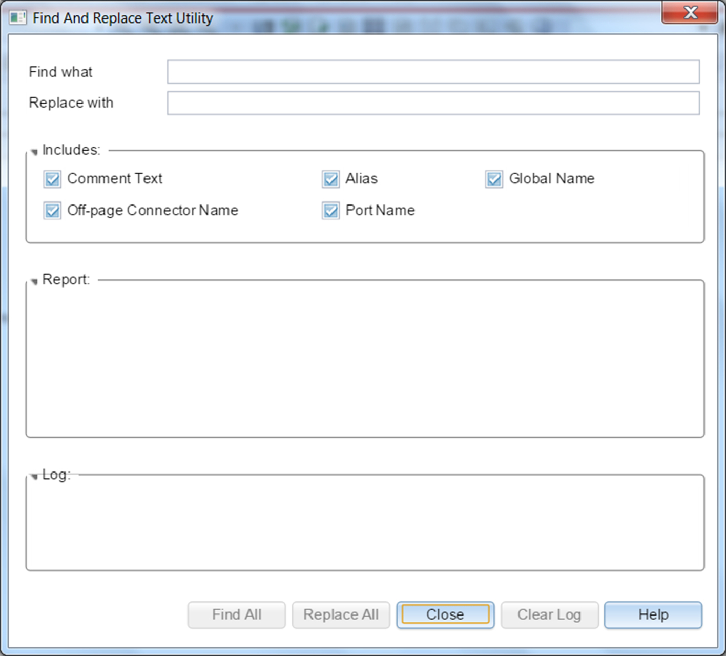
1.8.2 Find and Replace Text Utility
Capture already has a Find and Replace function (Edit > Replace) of text but in 17.2, the Find and Replace Text Utility can find and replace text from global names, nets, ports, comments, and of page connectors (see Fig. 1.24). The report section provides information on the text type and location, whereas a log file gives a summary of the action taken. You can search the entire design or the current page you are working on and then select from the top tool bar, Tools > Utilities > Find ReplaceText.
1.8.3 Password Protection
In 17.2, Capture designs can be password protected but a word of warning, lost passwords cannot be retrieved even by Cadence. This function is not available in the 17.2 Lite version only in the full version. Passwords can be set by either Design > Set Password or highlighting the dsn file in the Project Manager and rmb > Set Password. Other options include removing or changing the password.
1.9 Summary
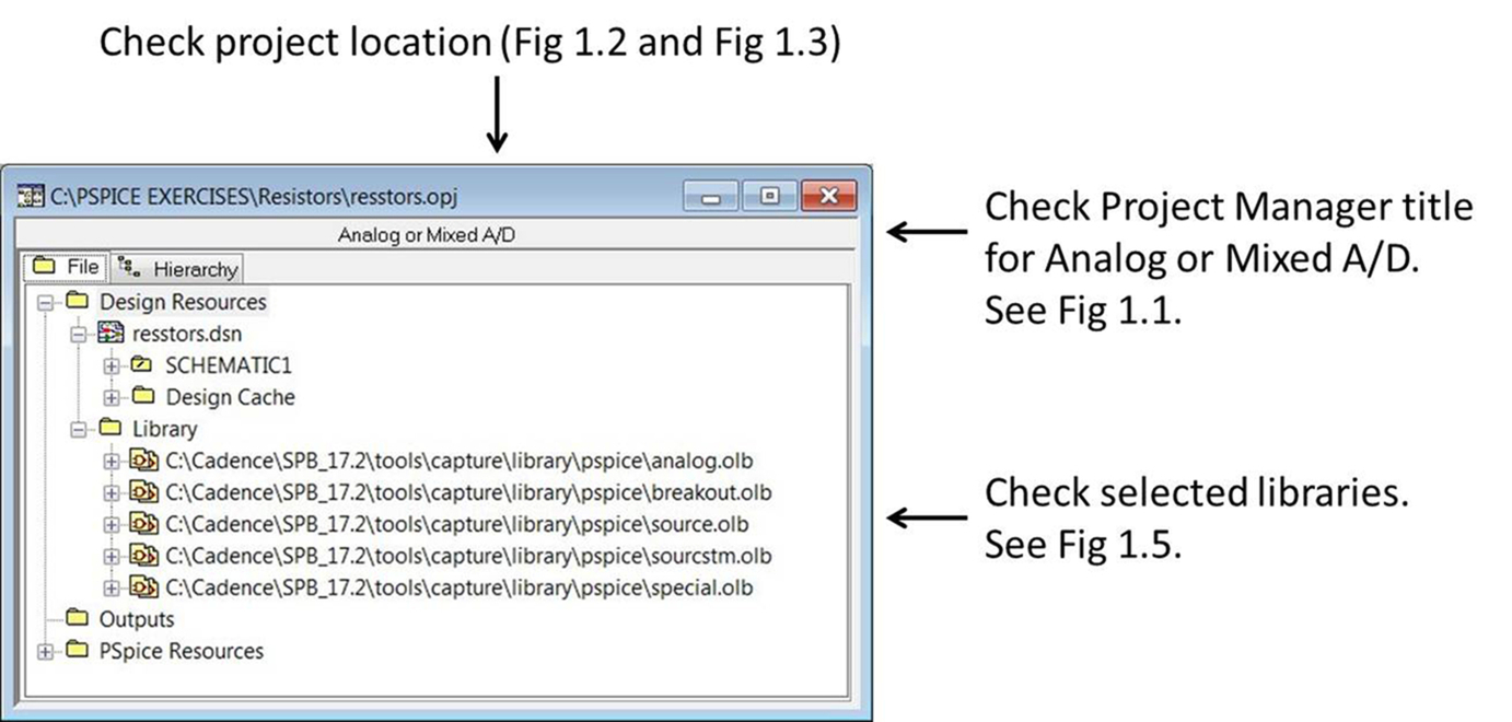
Fig. 1.25 shows the Project Manager created for a PSpice project and the visual checks that can be made to ensure that a PSpice project has been setup correctly. One common mistake is not selecting and highlighting the project folder that is created (see Fig. 1.4).
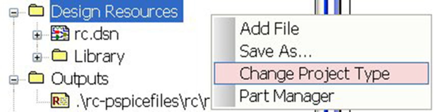
Another common mistake when creating a project is that the wrong project type has been created, for example you see PCB instead of Analog or Mixed A/D in the Project Manager title. One way around this is to create a new project (of the correct type) and copy and paste the .dsn file from the previous Project Manager into the new Project Manager. From version 16.3 onward, you can now change the project type by highlighting Design Resources in the Project Manager and right mouse button, rmb > Change Project Type, see Fig. 1.26.
1.10 Exercises
Exercise 1
You will create a new PSpice project as discussed in section 1.2 and name it resistors. The project will be created in a folder called, for example, C:PSpice Exercises esistors and will be configured with the simple five default libraries.
1. You can select the New Project icon  , or select File > New > Project. Enter resistors for the Name and select Analog or Mixed A/D. In Location, enter C:PSpice exercises
esistors or you can browse to your own folder location. Check your entries with Fig. 1.27 and then click on OK.
, or select File > New > Project. Enter resistors for the Name and select Analog or Mixed A/D. In Location, enter C:PSpice exercises
esistors or you can browse to your own folder location. Check your entries with Fig. 1.27 and then click on OK.
2. In the Create PSpice Project, select simple.opj as shown in Fig. 1.28 and click on OK.

3. The Project Manager window will appear as shown in Fig. 1.29.

4. Expand resistors.dsn by double clicking on it to open SCHEMATIC1 folder (Fig. 1.30).

5. Double click on SCHEMATIC1 to open PAGE1 and double click on PAGE1 to open up the schematic page (Fig. 1.31).

6. When you first open the schematic page, you will see some preplaced text and two voltage sources preplaced. Delete the sources and text by drawing a box around the sources and text and press the delete the key.
Exercise 2
You will draw the resistor network shown in Fig. 1.32.

1. To place a resistor, select Place > Part and select an R from the analog.olb library. Double click on the R and the resistor will attach to the cursor. In previous versions you click on OK and the Place Part menu disappears. From release 16 onward, when you double click on a part or click on the Place Part  , the menu will remain open.
When you place the first resistor in the schematic, another resistor will be attached to the cursor, click on the right mouse button, rmb > Rotate or press R on the keyboard and place the second resistor. To exit place part mode, rmb > End Mode or press escape.
Whenever a part is selected, there is a rmb context menu for place part options.
P is the hotkey to place a part or you can select the Place Part icons depending on which software release you have 
 .
.
2. For R1 and R2, double click on the default resistor value of 1k and change its value to 10R.
3. Place the voltage source which can be found in the source library. Change its voltage to 10 V.
4. To place a ground symbol, Place > Ground (or press G) or click on the icon 
 and select the 0 V symbol from the capsym.olb library (Fig. 1.33).

5. To draw a wire, Place > Wire (or select the wire icon 
 or press W). You can always zoom in by pressing the “I” key on the keyboard or “O” for zoom out.
Note
To exit out of wire mode, you can press escape (Esc) on the keyboard or press W on the keyboard which toggles wire mode on and off. If you make a mistake you can always select the undo icon  .
.
Note
There are new features available from version 16.3 onward to automatically connect wires to two or more points and a feature to automatically connect wires to a bus which is described in the Chapter on Digital Simulation. To automatically draw a wire, select Place > Auto Wire > Two Points (Fig. 1.34) or click on the icon  . Click on the first wire point and then click on the second point.

6. Capture automatically labels each wire connection also known as a node with a node number which by default is not displayed on the schematic. However, you can assign your own labels to wire nodes which will give meaning to a node, i.e., input or output and is useful when you want to analyze different nodes in a circuit. These labels are known as “Net Alias” and are placed on a wire by highlighting a wire and then selecting, Place > Net Alias (or select the net alias icon 
 or press N).
7. Save the project by selecting File > Save.
Note
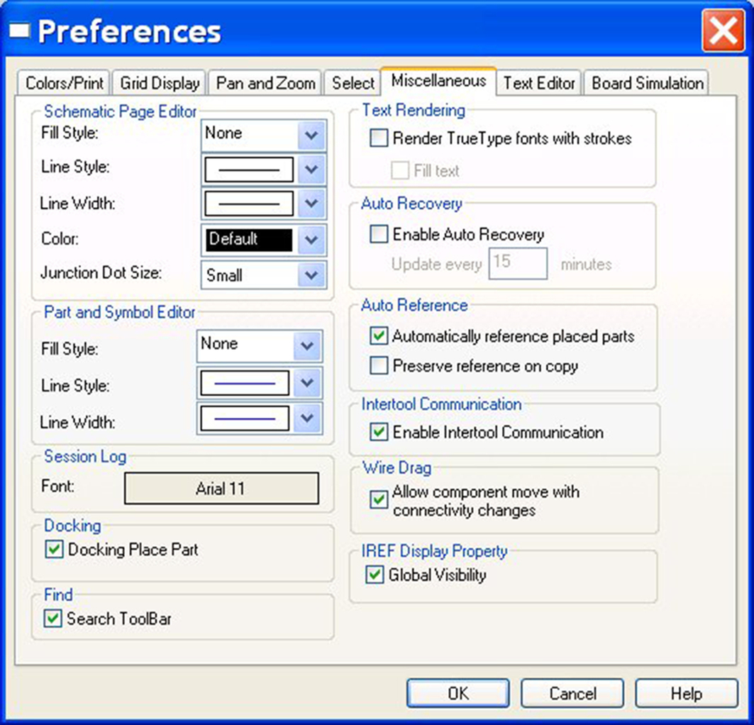
Parts can be pushed together such that when you move the parts away, wires are automatically connected. If not already set, select, Options > Preferences > Miscellaneous > Wire Drag and check, Allow component move with connectivity changes on as shown in Fig. 1.35. This also allows parts to be moved onto a wire and be connected.
1.11 Extra Library Work
1. Select Place Part to open the Place Part window and Add Library by clicking on the  icon, see Fig. 1.36. In previous versions, you just click on Add Library (see Fig. 1.10A).

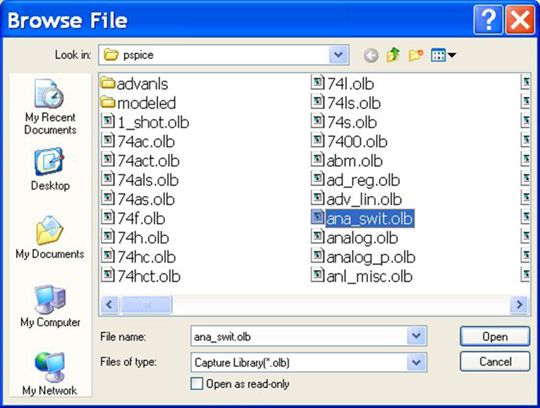
2. The Browse File window (Fig. 1.37) will open. Make sure you are in the < install path > tools > capture > library > pspice and select the ana_swit.olb library and click on Open.
3. Close Place Part. Has the library been added to the library list in the Project Manager? Expand the Library folder.
4. In the Project Manager select the Library folder and right mouse button > Add File (Fig. 1.38).

The Browse File window will open as in step 2. Make sure you are in the < install path > tools > capture > library > pspice and select the 1_shot.olb library and click on Open.
5. Select Place Part. Has the 1_shot.olb library been added to the list of Libraries?
6. In Place Part select all the libraries and click on Remove Library. Note which libraries are now available.
As you create new projects, any libraries added to previous projects in Place Part will be added to the list of available libraries. However, these libraries are not added to the Project Manager. Only libraries added via the Library folder in the Project Manager will be added to the configured list of Project libraries and can only be deleted via the Project Manager.
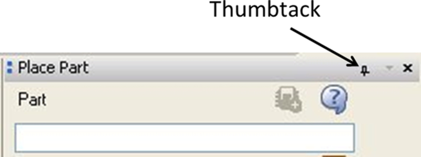
From 16.2 onward, when you select Place Part, the menu appears on the right hand side of the schematic and reduces the available size of the schematic page. However, at the top right of the Place Part menu, there is a thumbtack icon (Fig. 1.39) which gives you the option to effectively hide the Place Part menu. When you select the thumbtack icon, the Place Part menu disappears and the words Place Part appears as shown in Fig. 1.40. The menu re-appears when you move the mouse inside the Place Part window box and retracts when you move the mouse back to the left.