
5
First Assembly Language Program
![]() Problem statement
Problem statement
![]() Approach methodology
Approach methodology
![]() Program
Program
![]() Explanation of the program
Explanation of the program
![]() About the microprocessor kit
About the microprocessor kit
![]() Major components of a kit
Major components of a kit
![]() Functions performed by a microprocessor kit
Functions performed by a microprocessor kit
![]() Major components of ALS-SDA-85M kit
Major components of ALS-SDA-85M kit
![]() Opcode of an instruction mnemonic
Opcode of an instruction mnemonic
![]() Basics of using the kit
Basics of using the kit
![]() Entering the program
Entering the program
![]() Entering the data
Entering the data
![]() Executing the program without a break
Executing the program without a break
![]() Executing the program in mode single step
Executing the program in mode single step
![]() Using a kit other than ALS-SDA-85M kit
Using a kit other than ALS-SDA-85M kit
![]() Using the microprocessor kit in serial mode
Using the microprocessor kit in serial mode
![]() Questions
Questions
Now that we have an idea of the programmer's view of 8085, let us see how it can be used to solve problems for us. To explain this aspect, let us consider a very simple problem.
 5.1 PROBLEM STATEMENT
Let us say, we have some 8-bit number in a symbolic memory location X. We want to compute its 2's complement and store the result in symbolic memory location Y, overwriting the previous contents of memory location Y.
5.1.1 APPROACH METHODOLOGY
We need to have memory locations X and Y in the RAM area of the kit. The RAM space in the kit is F800H to FFFFH. So let us arbitrarily choose X as memory location F840H, and Y as memory location F850H.
Let us say, we have in memory location F840H the 8-bit number 12H (i.e. 0001 0010). To find its 2's complement, first of all we have to find its 1's complement, and then add 1 to it. The 1's complement is EDH. Thus the 2's complement becomes EEH. Finally this result is stored in memory location F850H. This is diagrammatically indicated in Fig. 5.1.
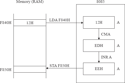
Fig. 5.1 Finding 2's complement of a number
5.1.2 PROGRAM
There is nothing like a unique program for solving a problem. However, there will exist a program that is optimal considering one or more of the following factors: ease of developing the program; size of program; and speed of execution of program.
In this book, the programs are written giving highest priority for ease of writing the program, followed by size of program, and finally speed of execution is considered. This is because, speed of execution is most important only in real-time applications, like firing a missile. It is required to minimize size of program, only when the program is too big for the computer's memory. In the present-day world, memory has become very cheap of late. Ease of developing program is very important, because manpower is becoming increasingly expensive.
Program to solve this simple problem is as follows.
LDA F840H     ; (A) = 12H
            CMA           ; (A) = EDH
            INR A         ; (A) = EDH
            STA F850H     ; (F850) = EEH
            HLT
5.1.3 EXPLANATION OF THE PROGRAM
Explanation for each of the lines of the program is given as follows.
Line 1—LDA F840H: Finding the 1's complement is done by changing 0s to 1s and 1s to 0s. This is a logical invert or negate operation. In a microcomputer the logic unit of the ALU can only perform this operation. The ALU is inside the microprocessor. So, first of all the number from memory location F840H has to be brought to the microprocessor. But then, which register in 8085 should receive it? As described earlier, Accumulator is the most important 8-bit register, and so it is desired to receive it in Accumulator. This is achieved by executing the instruction ‘LDA F840H’.
Here, LDA stands for ‘LoaD the Accumulator from memory location’. Just LDA is meaningless. LDA must be followed by a 16-bit memory address to make sense. We say, ‘LDA’ is the mnemonic for ‘load the accumulator from memory location’. Such mnemonics are designed to help us memorize the actual expansion.
Notice that the first line, as well as other lines of the program, have some more information written after a semicolon. Whatever follows a semicolon is to be treated as a comment only. It is not part of the instruction. It is optional. However, it makes the program easier to understand.
Thus, in the first line ‘(A) = 12H’ is to be treated as a comment. In this book ‘()’ stands for ‘contents of’. Thus, ‘(A) = 12H’ is to be read as ‘contents of A becomes 12H’. In other words, LDA F840H results in A register content becoming 12H.
Line 2—CMA: Finding the 1's complement of the number in Accumulator is achieved by executing the CMA instruction. Here, CMA is the mnemonic for ‘CoMplement the Accumulator’. The result of this operation will again be stored in the accumulator. Thus, Accumulator value changes to EDH, as indicated in the comment part of this line. In 8085, only Accumulator contents can be complemented. In fact, that was the reason for bringing the number from memory location F840H to Accumulator, and not any other register.
Line 3—INR A: Adding 1 to the number in the accumulator is achieved by executing the INR A instruction. Here, INR A is the mnemonic for ‘INcRement the Accumulator’. The result of this operation will again be stored in the Accumulator. Thus, Accumulator value changes to EEH, as indicated in the comment part of this line. Thus, we now have in the Accumulator, the 2's complement of the number at memory location F840H.
Line 4—STA F850H: This instruction stores the Accumulator contents in memory location F850H. Here, STA is the mnemonic for ‘STore the Accumulator contents in memory location’. Just STA is meaningless. STA must be followed by a 16-bit memory address, like F850H, to make sense. Thus, contents of memory location F850H changes to EEH, as indicated in the comment part of this line. Now the objective of the program is achieved.
Line 5—HLT: ‘HLT’ is the mnemonic for ‘Halt the processor’. Thus, when this instruction is executed, the processor halts. The reader may be wondering as to why this instruction is necessary at all. The reader may think that once the job is done the processor has to stop without being told so. But, a microprocessor keeps on executing instruction after instruction, unless asked to halt! It is very much unlike a human being, who unless ordered to work, is always whiling away his time!
5.2 ABOUT THE MICROPROCESSOR KIT
To execute the previous program we need a microcomputer. A microprocessor kit is a tool to develop and test user programs. It is quite often called ‘μP kit’ or simply ‘kit’.
5.2.1 MAJOR COMPONENTS OF A KIT
As it is basically a microcomputer, it will have the following.
- 8085 as the microprocessor,
- EPROM to store the monitor program, also called control program,
- Keyboard using which the user can enter his program and data,
- RAM to store user program, data, as well as results,
- Seven-segment LED display, to indicate memory address and contents,
- I/O ports to communicate with peripheral devices, etc.
5.2.2 FUNCTIONS PERFORMED BY A MICROPROCESSOR KIT
A kit has in-built features to allow a user to perform the following.
- Enter program and data using the keyboard;
- Execute the program without any break;
- Run the program in single step (useful for detecting errors);
- Examine, and if needed modify, register values;
- Examine, and if needed modify, memory contents;
- Examine, and if needed modify, next/previous memory contents;
- Perform insertion/deletion of bytes in the user program;
- Perform movement of a block of information, etc.
The above features are provided by the monitor program stored in the EPROM. In addition to the above mentioned features, the monitor program provides a number of utility routines also. These routines help in easy program development. The utilities generally provided on the EPROM are: time delay routine; routine to display information on the data and address fields; routine to read from the keyboard, etc.
When Intel developed 8085 microprocessor, they also released SDK-85 (system design kit for 8085). This was the first 8085 microprocessor kit. Subsequently, a number of system integrators have come out with their versions of the 8085 kit. These later versions are superior in their features compared with the SDK-85. In this book, for the purposes of explanation, we have chosen ALS-SDA-85M trainer kit developed by M/s Advanced Electronic Systems, based in Bangalore. Henceforth, by ‘kit’ we mean ALS-SDA-85M trainer kit.
5.2.3 MAJOR COMPONENTS OF ALS-SDA-85M KIT
Major components of ALS-SDA-85M kit are the following.
- 8085 CPU operating at 3 MHz (approx.),
- 27128 EPROM (capacity 16K bytes, address range 0000H-3FFFH),
- 6116 RAM (capacity 2K bytes, address range F800H-FFFFH),
- Two 8255s (provides 48 I/O lines),
- Keyboard having 28 keys (0 to F, subst mem, next, prev, etc.),
- Six seven-segment LEDs (four for address field, two for data field),
- 8279 (used for interfacing the keyboard and seven-segment displays),
- 8253 (provides three 16-bit timers),
- 8251 (provides serial interface to connect to a host computer), etc.
The component layout diagram of the ALS kit is shown in Fig. 5.2. The working of all these ICs, and the kit will be discussed in detail in later chapters.
5.2.4 OPCODE OF AN INSTRUCTION MNEMONIC
First of all, notice that to enter an instruction like ‘CMA’, we do not have the ‘M’ key, or to enter an instruction like ‘HLT’, there is no ‘T’ key. Then, how to enter such instructions? It was explained earlier that a digital computer understands only 0s and 1s. So, we have to input an instruction to the computer using only 0s and 1s. Thus, instead of typing the mnemonic ‘CMA’, we have to enter ‘0010 1111’, which is the operation code for the mnemonic CMA. An operation code is also called ‘opcode’ for short.
Entering 8 bits like this is very tedious. So the kit is provided with a hex keyboard, using which we are allowed to input in hexadecimal. Thus instead of typing ‘0010 1111’, we enter only the two characters ‘2F’ using the keyboard. However, it should be borne in mind that what is stored inside the computer is the binary value 0010 1111.
Similarly, every instruction mnemonic has a corresponding 8-bit opcode, which is entered using the keyboard as two-digit hexadecimal value. The programmer is not required to memorize the opcodes for the various instructions. He is provided with a chart indicating the opcodes for the various instructions. Fig. 5.3 provides the opcodes in hexadecimal for the instruction mnemonics, arranged in alphabetical order.
Instruction length in 8085 can be 1 byte, 2 bytes, or even 3 bytes, although the opcode is always 1-byte long. For example, CMA is only 1-byte long, whereas LDA F840H is 3-bytes long. In LDA F840H, the opcode for LDA is 1-byte long and F840H occupies another 2 bytes. With this information, now we are ready to use the kit.
5.2.5 BASICS OF USING THE KIT
Do we store our program in EPROM or RAM? The advantage of storing it in EPROM would be that the program will not be lost, when power supply fails. But the disadvantage is that we have to use an EPROM programmer to enter the program. If RAM is used, the program can be easily entered, but the disadvantage is that it will be lost if power supply fails. But we decide to store it in RAM for the following reasons.
- It is easy to enter it in RAM.
- It is not required to have this program in memory forever or for a long period. We do not mind losing the program once the result is obtained.
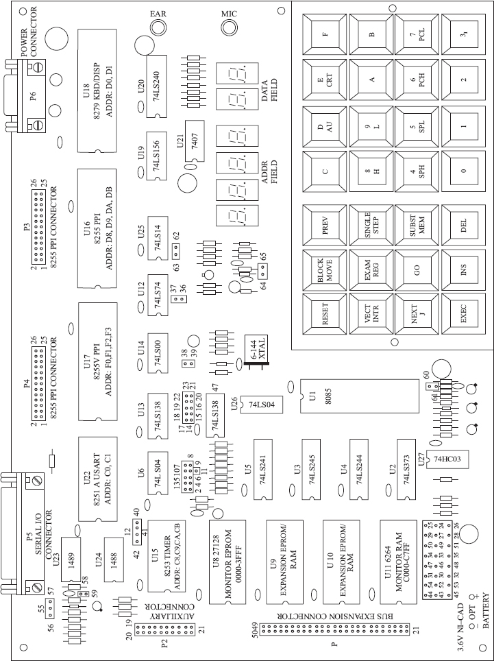
Fig. 5.2 Component layout of ALS-SDA-85M trainer kit
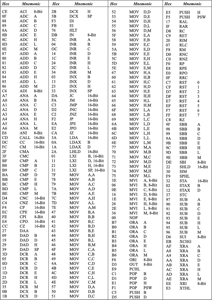
Fig. 5.3 Opcode chart for the instruction mnemonics
In ALS-SDA-85M, user program can be stored anywhere in the RAM address range of F800H to FFA0H. Memory locations FFA1H to FFFFH in the RAM are used by the monitor program for storing system variables. As such, the user should avoid this range for storing his program, data, or results.
To enter information in memory, the user has to go through the following steps.
Connecting the power supply: The kit uses power supply module 85M-OPT-04, which provides +5 V dc at 1 A, and ±12 V dc at 0.1 A. Connect power supply to the kit using the cable that is terminated with a nine-pin D-type connector at the kit end. Only two wires are required to be connected at this point. Generally orange, blue, or a white coloured wire is to be connected to the +5 V dc terminal and black coloured wire is to be connected to the ground terminal, marked as ‘COM’ (for common) on the power supply unit. The other wires are to be left open at this stage. They are needed to connect ±12 V dc to the kit, when it is desired to connect the kit to a host computer.
Sign-on message: Switch on the power supply. If the kit is working fine, it will display ‘-SdA 85’ on the six seven-segment LEDs. The ‘-’ in the beginning indicates that it is ready to accept user commands. It is generally called the system prompt. ‘-SdA 85’ is the sign on message that is displayed whenever power is switched on, or whenever the ‘reset’ key is typed.
Checking contents of a memory location: Type the key ‘subst mem’. It stands for ‘substitute memory’. A dot is displayed at the right edge of the address field. Except for the dot, the address and data fields will be blank. It indicates that the kit expects the user to type a four-hex digit address value. If the user wants to see the contents of F820, he has to type the keys ‘F’, ‘8’, ‘2’, ‘0’ one after another. The display in the address field after each of the above typing will be ‘000F.’, ‘00F8.’, ‘0F82.’, and finally ‘F820.’.
Notice that the ‘.’ is still at the edge of the address field. It means that the user can still change the address value if he desires, by typing the new address. Let us say, we are interested in contents of F820H. Then type ‘next’ key. Then the display in the data field indicates the contents of memory location F820H. Suppose, memory location F820 is having the value 3E, the display after typing ‘next’ key will be ‘F820 3E.’. The typing needed to check contents of location F820H is indicated in Fig. 5.4. In this Fig. ‘=’ stands for a blank character.
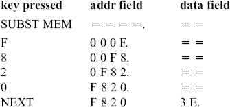
Fig. 5.4 Typing needed to check contents of location F820H
Changing the contents of a memory location: Notice that the ‘.’ is now at the edge of the data field. It means that, if the user wants to change the data, he is free to do so. Suppose we want to change the contents of F820H to 47H, then type ‘4’ and ‘7’. The display in the data field after each of the above typing will be ‘04.’, and finally ‘47.’. Notice that the ‘.’ is still at the edge of the data field. It means that the user can still change the data value if he desires, by typing the new data.
Let us say, the user decides to change the data to 3A. Then, type ‘3’ and ‘A’. The display in the data field after each of the above typing will be ‘73.’, and finally ‘3A.’. Notice that the ‘.’ is still at the edge of the data field. It means that the user can still change the data value if he desires, by typing the new data. Let us say, the user is not interested in any more change. Then type ‘next’ key. Only now, the monitor program stores in memory location F820H the value 3AH. Then the display changes to indicate the contents of the next memory location F821H. For example, if location F821H is having the value BEH, the display will become ‘F821 bE’.
If the user wants to change the contents of F821H to 40H, he has to now type ‘4’, ‘0’, and finally ‘next’. Then 40H is entered into memory location F821H, and the display indicates the contents of location F822H. If the user wants to change the contents of F822H to F8H, he has to now type ‘F’, ‘8’, and finally ‘next’. Then F8H is entered into memory location F822H, and the display indicates the contents of location F823H. If the user is not interested in entering any more information, he has to type ‘exec’ key, to terminate the process of storing information in memory. Power supply is switched off, when there is nothing else to be done on the kit. But then, the information stored in the RAM will be lost.
The typing required to first change the contents of F820H to 47H, and then to 3AH, contents of F821H to 40H, and contents of F822H to F8H is shown in Fig. 5.5. In this diagram ‘d d’ in the data field indicates any arbitrary two-digit hex value, which is not of interest to us.
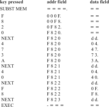
Fig. 5.5 Typing needed to modify contents of locations F820H, F821H, and F822H
5.2.6 ENTERING THE PROGRAM
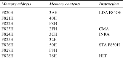
As an example, let us store the program in section 5.1.2 starting from F820H. The first instruction of our program, LDA F840H, occupies 3bytes in memory. Notice that in 8085 programs, a 16-bit memory address like F840H, has to be stored in memory in byte reversal form. In this example, 40, which is the LS byte has to be stored in the lower address F821H, and F8, which is the MS byte has to be stored in the higher address F822H. Thus, LDA F840H has to be stored as 3A 40 F8 in the three locations starting from F820H, as shown in Fig. 5.5. Here 3A is the opcode for LDA. There are microprocessors like Motorola 6800, where 16-bit addresses are not stored in memory in byte reversal form. But somehow, in all Intel processors 16-bit addresses are required to be stored in byte reversal form. This notation of storing addresses in memory is known as little endian notation. The notation used in Motorola processors is known as big endian notation.
The second instruction in the program, CMA, occupies only 1 byte in memory. It is stored as 2F in the memory location F823H. The third instruction in the program, INR A, also occupies only 1 byte in memory. It is stored as 3C in the memory location F824H. The fourth instruction in the program, STA F850H, occupies 3bytes in memory. It is stored as 32 50 F8 starting from memory locations F825H. Finally, the last instruction in the program, HLT, occupies only 1 byte in memory. It is stored as 76 in the memory location F828H.
This program stored in memory using opcodes is called the machine language program. The machine language program is shown in the following.
The typing required on the keyboard to enter the program is shown in Fig. 5.6.
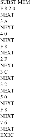
Fig. 5.6 Typing required on the keyboard to enter the program
5.2.7 ENTERING THE DATA
Now that the program is stored in memory, it is now necessary to store in memory the data on which the program is to operate. As this program takes the data from memory location F840H, we store in this location the data value. If we wish to compute 2's complement of 12H, we store 12H in F840H by typing the keys as shown in Fig. 5.7.
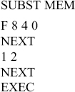
Fig. 5.7 Typing required on the keyboard to enter the data
5.2.8 EXECUTING THE PROGRAM WITHOUT A BREAK
Now the program and data are in memory. To execute the program, we have to just type the keys as shown in Fig. 5.8. In this diagram ‘a a a a’ in the address field indicates any arbitrary four-digit hex value, which is not of interest to us. Similarly, ‘d d’ in the data field indicates any arbitrary two-digit hex value.
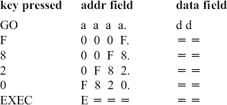
Fig. 5.8 Typing required executing the program without break
Notice that once the program is executed, it displays ‘E’. Here, ‘E’ stands for ‘executed’. Of course, many mistake it to mean ‘error’! Then to check the result of execution, we have to just look at the contents of memory location F850H. This is done by typing
- RESET
- SUBST MEM
- F 8 5 0
- NEXT
As the data for the program is 12H, its 2's complement is EEH. So, if we get EE displayed in the data field now, we have got the correct answer.
In this example, we have run the entire program without a break. After this, it is a good practice to check up the program with several different data. But every time we change the data, we have to run the program again, and then only we should check the contents of F850H to see the result.
5.2.9 EXECUTING THE PROGRAM IN SINGLE STEP MODE
In the previous example, if the result is not EE, it means that the program has not produced correct 2's complement. This will be so, when the program is wrong. To locate the error, the facility provided in a kit is the single-step feature.
Using single-step feature, the programmer can see the contents of memory locations, or registers, after the execution of each instruction in the program. If needed, he can even alter the contents of memory locations or registers, after the execution of each instruction. If the user is not interested in seeing the contents of memory locations or registers, he can simply proceed with the next instruction.
To use this feature, the user should first of all note down the effect of execution of each of the instruction in the comments field. This is called ‘tracing’ the program execution. For example, he should note that A register content should change to 12H, after the execution of LDA F840H. If after executing LDA F840H, register A has the value 34H, something is wrong with this instruction. Then the user should carefully check the coding of the instruction. A common mistake is coding LDA F840H as ‘3A F8 40’, instead of the correct code, which is ‘3A 40 F8’. Other possible mistakes could be wrong typing of code for LDA. The user by mistake may type ‘4A’ or ‘3B’, instead of the correct code ‘3A’.
If the tracing of the program gives wrong answer, it is definite that the program is incorrect. If the tracing of the program gives correct answer, it is likely that the program works correctly for all possible values of input data. The user should verify this by giving different sets of data in a judicious way.
To check the program in single step mode, type the keys as shown in Fig. 5.9 when the system prompt appears in the address field.
In the single-step mode, after checking contents of a register, the other sequential registers can be checked by just typing ‘NEXT’ every time, finally terminating the command by typing ‘EXEC’. For example, if the user is only interested in checking contents of H and L registers at the end of execution of an instruction. he has to type the following.
- EXAM REG
- H (displays H register contents in the data field)
- NEXT (displays L register contents in the data field)
- EXEC (terminates the ‘exam reg’ command)
In this, notice that to display contents of H register the key on which both H and 8 are printed has to be typed. After typing ‘EXAM REG’, if this key is typed, it is interpreted as H. Similarly, after typing ‘SUBST MEM’, if this key is typed, it is interpreted as 8. There are some more keys on the keyboard, which have two values engraved.
Similarly, in the single-step mode, after checking contents of a memory location, the other sequential locations can be checked by just typing ‘NEXT’ every time, finally terminating the command by typing ‘EXEC’. For example, if the user is only interested in checking contents of memory locations F850H, F851H, and F852H at the end of execution of an instruction, he has to type the following.
- SUBST MEM
- F 8 5 0 (displays F850 in the address field)
- NEXT (displays contents of F850 in the data field)
- NEXT (displays contents of F851 in the data field)
- NEXT (displays contents of F852 in the data field)
- EXEC (terminates the ‘subst mem’ command)
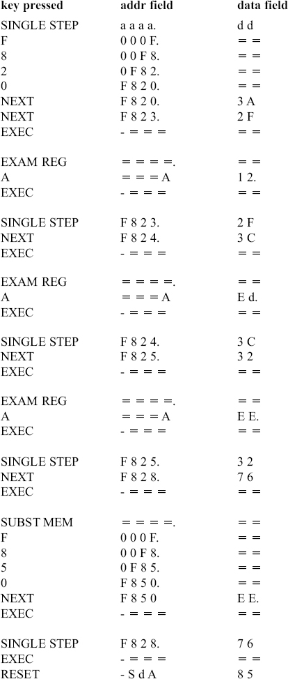
Fig. 5.9 Typing needed to trace the program in single step mode
5.2.10 USING A KIT OTHER THAN ALS-SDA-85M
When the user has access to a kit by some other manufacturer, there are likely be to some differences in the features compared with the ALS-SDA-85M kit. The differences are likely to be in the following details.
- EPROM capacity and address range,
- RAM capacity and address range,
- Number of I/O ports and their address,
- Utility routines and their addresses,
- Availability of special peripheral chips and their addresses, and
- Differences in naming of some keys.
The user is required to go through the manual for the kit to get the necessary information.
5.3 USING THE MICROPROCESSOR KIT IN SERIAL MODE
So far we have discussed the use of the kit in the keyboard mode. In this case, the user has to translate the assembly language program into machine code, and enter the program in hexadecimal using the keyboard. This translation is quite monotonous, especially when the program is quite long.
If we have a computer with an ASCII keyboard, the program can be entered into computer memory straightaway as an assembly language program. Then, the assembler program in the computer can translate this assembly language program to machine code, relieving the user from this monotonous task. The machine code can finally be downloaded from the computer to the kit using RS-232C serial link. The user can then execute the downloaded program on the kit.
Also, the user can upload a machine language program from the memory of the kit to the hard disk or the floppy disk on the computer. The hard disk or floppy disk is non-volatile, which means it does not lose the information even after power is switched off and then turned on. Thus the user programs can be stored as disk files on the computer, for downloading later to the kit for execution. However, the cost goes up in serial mode, as a computer is a must in addition to the kit. Also, there must be assembler software on the computer. The circuitry and the monitor software on the kit also is increased.
The actual procedure for using the kit in serial mode is explained in a later chapter.
- What are the factors to be considered while developing a program?
- What is a microprocessor kit? Describe the main features of a typical microprocessor kit.
- What is an opcode? What is the size of an opcode, and an instruction in 8085?
- What is the need for single stepping through a program? What are the features provided by the single-step function?
- What is the advantage of using the kit in serial mode? What is the principle of its working?