
15
Regulating Diodes and Applications
OBJECTIVES: After studying this chapter, you will be able to
- Describe what a zener diode is
- Describe the differences between a regular diode and a zener diode
- Use a zener diode in a circuit
- Define how to combine zener diodes and for what purpose
- Use a zener diode for voltage regulation
- Recognize a zener diode in a circuit
- Describe what a diac is and what it is used for
- Explain the characteristics of a diac
- Describe the application of a silicon-controlled rectifier (SCR)
- Define the difference between a diode and a SCR
- Describe the relationship between diac and triac
- Recognize the application of a triac
- Draw circuit diagrams the professional way
New terms: Breakover voltage, diac, silicon-controlled rectifier (SCR), triac, voltage regulation, zener current, zener knee, zener region
15.1 Introduction
In Chapters 16 to 21, some electronic devices, which are more pertinent to the objective of this book, will be explained. It is not the intention, nor within the scope of the book, to introduce all electronic devices. Nevertheless, because of their importance, two regulating diodes are discussed in this chapter. These two devices are used for voltage regulation in DC circuits and current regulation in AC circuits.
The zener diode is widely used for voltage regulation in DC circuitry. It is a diode with two layers of semiconductor material. The triac is another electronic device use in AC circuitry; it controls current for the soft start of motors and reducing inrush current, and operation of a dimmer switch, for instance. These two devices are not of the same category as far as their structure is concerned. But, because of their function, control and regulation, it is reasonable to include them in one chapter.
The triac is a switching device, meaning that it has a gate through which it can be turned on and off. Gated or switching devices are discussed in Chapter 19. They are used for various applications covered in Chapters 20 and 21.
Triac: Type of gated diode for alternative current. Its main terminals do not connect until the gate allows connection or the voltage across it has reached certain value.
15.2 Zener Diode
Similar to the ordinary diode that we discussed in Chapter 14, there are other types of diodes that are commonly and frequently used in electronic circuits for industrial and domestic applications. One of these is the zener diode.
The zener diode is a special type of diode that is designed to work in reverse bias and in the so-called zener region of the diode characteristic curve. This region is after the reverse-biased voltage has exceeded the breakdown voltage (breakdown point). If the reverse bias voltage is less than the breakdown voltage, or if the zener diode is forward biased, it acts as an ordinary diode. That is, in forward bias it allows current, and in reverse bias it blocks current. After this voltage has surpassed the breakdown point (in reverse bias), the diode falls in the zener region, where it conducts without getting damaged. Current in this region was called avalanche current in Chapter 14. For a zener diode it is also called zener current. As soon as the voltage decreases, the diode retains its nonconducting condition and gets back to its normal properties. This specific property of being operational in the reverse bias and with avalanche current is given to the zener diode by a rich doping of the semiconductor material. Moreover, by controlling the amount of doping, the thickness of the depletion region in the PN junction and the breakdown voltage can be set to any value.
Zener current: Same as the avalanche current (the higher current after breakdown occurs in a semiconductor device) in a zener diode.

Figure 15.1
Zener diode characteristic curve.
Zener knee: Sharp curve in the characteristic curve of a zener diode where the breakdown voltage is reached and breakdown occurs.
Zener region: Region in the characteristic curve of a zener diode where the breakdown has occurred because of the reverse voltage surpassing a certain value.
Figure 15.1 shows the characteristic curve of a zener diode, which is more or less similar to that of an ordinary diode. The range after the zener knee (breakdown voltage) until the rated voltage of a zener diode is reached is called the zener region. In this region a small change in voltage leads to a large change in current. For instance, a change of 1 V in voltage can cause the current to increase by 10 times.

Figure 15.2
Symbol for a zener diode.
A zener diode works when reverse biased. Otherwise, it behaves as an ordinary diode.
As can be understood from the characteristic curve, in this region, when the reverse voltage is smaller in absolute value than the zener breakdown voltage, the current is very small and confined to the so-called leakage current, which is negligible and can be ignored. But for higher reverse voltages, there is an abrupt and large increase in current. In other words, whereas the voltage remains almost constant, the current has a considerable variation. This is the significant property of a zener diode, which can be employed.
A zener diode has a different symbol to differentiate it from other diodes. This symbol is shown in Figure 15.2. The physical shape of a zener diode can be the same as that of a regular diode.
15.3 Zener Diode Application
The main application of a zener diode is in voltage regulation. Voltage regulation implies keeping a voltage at a desired value irrespective of current and other factors that tend to change it. It is very important for many devices to protect them from overvoltage (and excessive current, as a result). The specific property of a zener diode is that in its operating range the voltage drop across it is constant (it has an internal self-regulatory characteristic). This could be understood from the characteristic curve in Figure 15.1, which can be expressed differently: large current change in a zener diode causes only a small variation in voltage. That is, the voltage drop across it is almost constant. In this respect, if a zener diode is in parallel with another component, or device, the voltage across that device is kept constant, because of the zener diode.
Voltage regulation: Controlling electric voltage in a circuit or a device to remain within a desired range (small variation) under different load conditions.
The main application of a zener diode is in voltage regulation.
Figure 15.3 depicts a load in parallel with a zener diode, both in series with the 200 Ω resistor R. Notice the polarity of the zener diode. The role of the resistor R is to provide the leverage for current adjustment. The zener diode is a current governed device. If we remove R, the whole voltage is applied to the load.
Zener diodes come in different voltages, for example, 5.6, 7.5, 10, and 16 V, just to name a few. For each purpose the right size diode (voltage and rated current) must be employed (see Section 15.5 for a combination of zener diodes in series and parallel).

Figure 15.3
Zener diode in a circuit, regulating load voltage.
15.4 Application Examples
The following examples show the application of a zener diode and the concerns for the proper rating. Note the polarity of the circuits in the reverse biasing of the zener diode. If a zener diode is used in forward bias, it performs as a regular diode.
In all the examples, there is a resistor in series with the zener diode and the load. The zener diode is in parallel with the load. When necessary, we refer to this resistor as the series resistor.
If a zener diode is forward biased, it behaves as an ordinary diode.
Example 15.1
In Figure 15.4 the 100 Ω resistor is the load and the diode used is a 4.7 V zener diode. In each of the three cases, find the current in the load (note polarity difference of the zener diode in cases 2 and 3).
Solution
-
Following Ohm’s law the current is
I = 12 ÷ 150 = 0.08 A
The voltage drop in the 50 Ω resistor is (50)(0.08) = 4 V.
- The zener diode is forward biased, and it behaves as a regular diode. The voltage drop across it is only 0.7 V.
Current in the load = 0.7 ÷ 100 = 0.007 A = 7 mA
Current in the 50 Ω resistor = (12 − 0.7) ÷ 50 = 0.226 A = 226 mA
Current in the diode = 226 − 7 = 219 mA
- The zener diode is reverse biased and performs as a voltage regulator
Current in the load = 4.7 ÷ 100 = 0.047 A = 47 mA
Total circuit current = Current in the 50 Ω resistor = (12 − 4.7) ÷ 50 = 0.146 A = 146 mA
Current in the diode = 146 − 47 = 99 mA
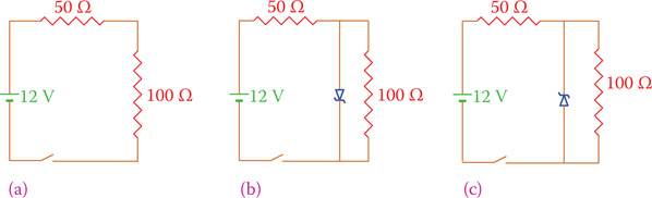
Figure 15.4
Example 15.1. (a) No zener diode in the circuit. (b) Zener diode is forward biased. (c) Zener diode is reverse biased.
Example 15.2
If the load in Example 15.1 is changed to 200 Ω, what is the change in the circuit current?
Solution
Circuit current is always the current in the 50 Ω resistor. In case 1, I = 12 ÷ 250 = 0.048 A. But, we get the same values for the circuit current in cases 2 and 3 as in Example 15.1, since in case 2 the load is shorted by the diode and in case 3 the zener diode regulates the voltage across the load to be 4.7 V, as before. The current in the load is, however, half of the previous values (for cases 2 and 3).
Example 15.3
If the value of the 50 Ω resistor in Example 15.1 is changed to 200 Ω, what is the change in the circuit current, in case 3 only?
Solution
The current in the 50 Ω resistor must always be greater than the load current because it is the sum of the current is the zener diode and the load. If we calculate the currents in the load and in the 50 Ω resistor, we have
Load current = 4.7 ÷ 100 = 0.047 A
Current in the 50 Ω resistor = (12 − 4.7) ÷ 200 = 0.036 A
But, we observe that this current is smaller than the load current; thus, this is not a possible case. A value of 200 Ω resistor is not acceptable.
Example 15.3 shows that in selecting a series resistor for inclusion in the circuit when a voltage regulator is used, care must be taken not to have an improper size resistor. In such a case the circuit does not function as desired. The action of a zener diode is that it absorbs the extra current of the circuit that would flow through the load. But, in the case of Example 15.3, there is no extra current.
For the circuit just discussed, the current is 12 ÷ 300 = 0.04 A and the zener diode does not play any role.
When using a zener diode, it is important to remember that
- Voltage across the load (in case the zener diode is removed) must be more than the zener diode value for voltage regulation to happen.
- Current in the series resistor (the total circuit current) must be higher than the load current.
- We cannot entirely eliminate the series resistor.
Example 15.4
For case 3 in Example 15.1, how much is the maximum value that the series resistance R can have?
Solution
Maximum value of the resistor R must be such that the current in R does not go below the load current. In this sense, minimum current in R is the load current. The load current, thus, can define the maximum value of this resistor.
VR = 12 − VZ = 12 − 4.7 = 7.3 V
IR = ILoad = 4.7 ÷ 100 = 0.047 A
R = 7.3 ÷ 0.047 = 155 Ω
For regulating the voltage across a load we cannot entirely eliminate the series resistor.
15.5 Zener Diodes in Series and Parallel
In the same way that diodes could be put in series, if a larger regulated voltage is required a number of (compatible) zener diodes can be put together in series. For example, in Figure 15.5, three zener diodes are put together to provide a larger regulated voltage for the load.
Also, it is possible to put zener diodes in parallel to increase the current capacity. Figure 15.6 depicts an example.
15.6 Diac and Triac
Diac and triac are two devices, usually used together for current control in AC circuits. The names are made based on “diode for AC” and “triode for AC.” Although you now know about solid-state diode, the counterpart of that in vacuum tubes was also called diode; a tube with two elements (electrodes) inside it, plus a heating element. That was a vacuum tube used for rectification. In conjunction with it, there were triode, tetrode, and pentode with 3, 4, and 5 electrodes inside the tube. These were used for amplification and other functions, which are performed by various transistors and other semiconductor devices nowadays.
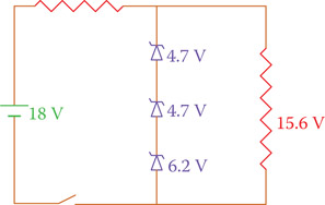
Figure 15.5
Zener diodes in series.
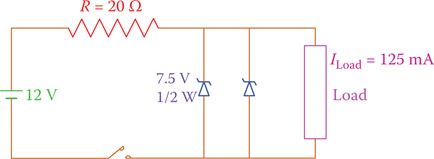
Figure 15.6
Zener diodes in parallel.
15.6.1 Diac
Diac is made up of three layers of N-type and P-type semiconductors, like a transistor (which are discussed in Chapter 17), but because of its doping it does not behave as a transistor. It is more like two antiparallel diodes (two diodes in reverse direction and parallel to each other). Thus, it is a bidirectional device and conducts in both directions, suitable for AC electricity. Nevertheless, it is not like two ordinary diodes, and conduction takes place when the applied voltage to it reaches a minimum value called breakover voltage (VBR).
Diac: Type of semiconductor device. It acts as a diode for alternating current, restricting the current until certain voltage is reached and then it conducts normally.
Breakover voltage: Voltage below which a diac or a triac is not conducting, but when the voltage surpasses that conduction starts.
The symbol and schematic structure of a diac are shown in Figure 15.7. As can be observed, a diac has no cathode and the two terminals are called anode 1 and anode 2, or alternatively MT1 and MT2. MT stands for main terminal.
Figure 15.8 shows the characteristic curve of a diac. It is a symmetrical curve, meaning that it behaves the same way for current in either direction. The breakover voltage of diacs is around 30 V (typically 20–40 V). When the applied voltage surpasses VBR, a diac sharply conducts and the current is abruptly increased. Later, if the current falls, conduction continues until the circuit current drops below the holding current (IH).
A diac is used for switching because it can deliver a sharp and clear signal when conduction starts. It serves for turning on the gate of a triac.
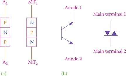
Figure 15.7
(a) Basic structure and (b) symbols for diac.

Figure 15.8
Diac characteristic curve.
15.6.2 Triac
Before learning about a triac, let’s describe a notation about a concept employed in many controlled semiconductor devices. A triac can be considered a member of a family of devices called silicon-controlled rectifier, abbreviated to SCR. In a later chapter we are going to learn more about SCRs and their applications, but here we want to introduce the concept of a gate. A silicon-controlled rectifier is like a diode with a gate. The gate is a control element through which the performance of a diode can be controlled. That is to say, unlike a normal diode, a silicon-controlled rectifier allows a current from its anode to its cathode only when the gate allows that. A silicon-controlled rectifier is a four-layer PNPN semiconductor, and it has three terminals, anode, cathode and gate.
Silicon-controlled rectifier (SCR): A family of gated diodes or transistors that can be controlled (turned on and off) through their gates.
Figure 15.9 illustrates the characteristic curve of a member of the SCR family. Considering only the forward bias half of the diac characteristic curve, this SCR has a similar performance except that with the current through the gate the behavior of the SCR changes. For this device a current flow from its anode to its cathode takes place only after the anode-cathode voltage has surpassed a minimum breakover voltage, but the breakover voltage is not fixed and can be controlled by the gate current IG.
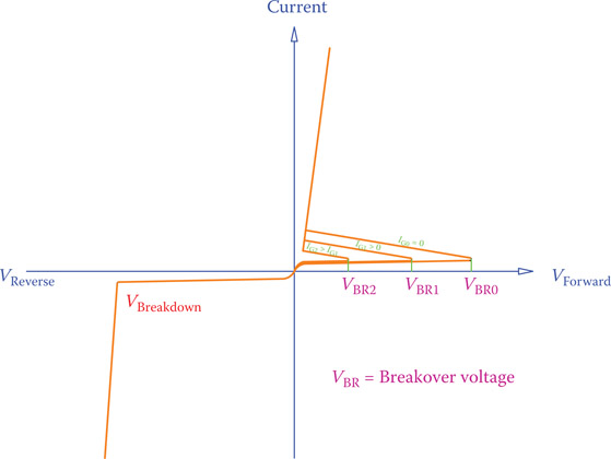
Figure 15.9
Characteristic curve of a silicon-controlled rectifier.
In Figure 15.9 the breakover voltage VBR0 is needed to start conduction in the SCR if the gate current IG is 0. For a positive IG1 the necessary voltage to start the SCR is VBR1, which is smaller than VBR0. Similarly, if the gate current increases to IG2, the device can start conducting at a lower breakover voltage VBR2. In this way the gate provides a means for control of the current through the SCR.
A triac is equivalent to two SCRs as shown in Figure 15.9 put antiparallel to each other and with their gates connected together. In this sense, it has three terminals, and it can perform in both directions, like a diac. We may say that a triac is a diac with a gate. Its performance in each direction is similar to a controllable diac, and it is used for AC electricity. Its terminals are called MT1 and MT2, or anode 1 and anode 2, similar to a diac. The schematics of its structure and its symbol are shown in Figure 15.10. As can be seen, its symbol is the same as that of a diac, with an added part for the gate.
Figure 15.11 shows one situation of the characteristic curve of a triac in comparison with that of a diac, which is almost symmetric for current in both directions. In order for a triac to be turned on, either a rather high voltage must be applied to it or it must be turned on by applying a voltage to its gate (see Figure 5.9). By changing the gate voltage, the minimum voltage between its two anodes (breakover voltage) to turn it on can be controlled.
Because a triac can work in either direction for current, its switching action falls into one of the following four modes: note that when A1 is connected to the mains positive terminal A2 is connected to the negative terminal and vice versa.

Figure 15.10
(a) Basic structure and (b) symbol of triac.

Figure 15.11
Characteristic curve of a triac.
- A1 is +, and gate signal is +
- A1 is +, but gate signal is −
- A1 is −, but gate signal is +
- A1 is −, and gate signal is −
A triac can work in all cases. Only the necessary gate signal is smaller in modes 1 and 4 because the voltage difference between anode 1 and anode 2 is similar to the voltage difference between the gate and anode 2.
Note that because the point of zero crossing of an AC waveform implies a zero current, a triac can turn off until the voltage across the anodes and the gate current allow conduction. In this sense, the general behavior of a triac can look as shown in Figure 15.12, for which the average voltage is smaller than if the current had a full waveform. This is the way that a triac can regulate the current in its circuit.
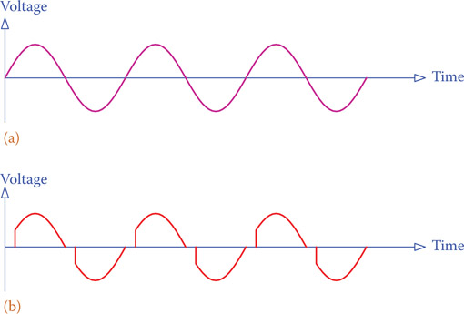
Figure 15.12
Effect of inserting a triac in an AC circuit. (a) Waveform without triac. (b) Waveform after triac is added.
Note that the waveform shown in Figure 15.12 is for a resistive load in the triac circuit. Phase shift is involved with inductive and capacitive loads.
Triacs are used for clean switching in place of electromechanical switches. They can be employed for soft starting of motors of small and medium size, particularly universal motors, lowering the inrush current in loads and many AC applications that need soft switching. High inrush current is possible for motors because their rotor initial rpm is zero, even for heating resistors and incandescent lightbulbs, because their resistance before they get hot is much lower. Among home appliances, the vacuum cleaner, refrigerator, washing machine, and so forth have universal motors that nowadays are controlled by triacs. A light dimmer also works with a triac, and the automatic voltage switch in many devices that must work with 120/220 V uses a triac.
There is a disadvantage with triac that they can turn on without being wanted by voltage spikes in the mains. Thus, this must be taken into account, and safety measures must be included for their usage in any electrical circuitry.
15.6.3 Testing a Triac
A triac can be tested by a meter. Either analog or digital meters may be used. Put the selector switch for resistance (ohm). Because a triac is an open circuit until it is turned on, a good triac shows a high resistance between its two terminals until it is triggered, when the high resistance falls to a small value or zero.
To test a triac, connect anode 2 of the triac to the positive (red) lead and anode 1 to the negative (black) lead. In fact, it does not matter how you connect, as long as the gate is free. The meter should read a large resistance or OL if a digital meter is used. For an analog meter it is recommended that first the meter is put on a large range ohm value, such as X100.
Now you connect the gate to anode 2 (if you know which one is anode 2) or to any of the terminals. The ohmmeter reading should go down to a small value (you may want to change to a smaller range on an analog meter for more precision). The reading should stay low even if you clear the gate connection.
Next, start over with swapping the red and black lead connections to the two anodes. The reading must show a high magnitude again. Make a connection between the gate and anode 2. Then the reading should fall and stay low, again, even if the gate connection is broken.
If the test results conform to the above description, the triac is good; otherwise, it is damaged. This test is good for typical triacs that do not have very sensitive gates. A small range (like X1) of an analog ohmmeter can damage a triac with very sensitive gate.
15.7 Presentation of Electronic Circuits Diagrams
Thus far in this book we have been following the common method for presenting an electrical or electronic circuit. This method is used for teaching because it facilitates the process of understanding the way components are in a circuit and the relationship between them (parallel, in series, having the same voltage, etc.). In industry, it is more customary to reduce the number of lines in a drawing by omitting the return line to the battery. This is particularly practiced for electronic circuits that usually contain more components. Instead, use is made of a common ground, where all the return lines to the power supply are shown as a connection to ground. In this way, the circuit of Figure 15.3 is depicted as in Figure 15.13. There is no difference between the two circuits, except the location of the switch, which is indeed better in Figure 15.13.
In Figure 15.13 the end of the 200 Ω resistor is connected to the positive side of a 24 V DC power supply, through the switch. The negative port of the power supply is connected to the circuit ground, which can be a chassis or a common point. Normally, the switch is not shown because it is a part of the power supply.
Hereafter, this way of presentation of circuits will be followed in the rest of the book.
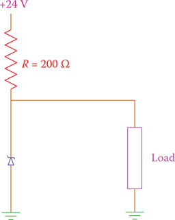
Figure 15.13
A more common way of exhibiting an electronic circuit.
15.8 Chapter Summary
- The main application of a zener diode is voltage regulation.
- A zener diode functions in reverse bias.
- If a zener diode is connected in forward bias configuration, it acts as an ordinary diode.
- The characteristic curve of a zener diode looks the same as that of an ordinary diode. The breakdown voltage is also called the zener knee.
- Voltage across a zener diode remains constant if a zener diode is subject to a higher (reverse bias) voltage across it. This constant depends on any particular diode.
- A load whose voltage is desired to be regulated is connected in parallel with a zener diode of the appropriate voltage.
- A zener diode cannot increase a voltage to regulate (the regulated voltage cannot be larger than the power supply voltage).
- Zener diodes come in various voltages and with different current ratings. A zener diode can be damaged if the current through it is over its current rating.
- Zener diodes can be put together in series to provide regulation for higher voltages (than their rating).
- Zener diodes can be put together in parallel to provide more current capacity for a circuit.
- A diac is like a diode for AC, but it conducts only if the voltage across its terminals reaches a certain level called the breakover voltage.
- When a diac conducts, it continues conduction as long as its current does not fall below the holding current.
- SCR stands for silicon-controlled rectifier. It behaves like a diode, but with a control capability through its gate.
- A triac behaves like a gated diac. It can be turned on by applying a voltage to its gate.
- A triac is used for current control of AC loads.
- Many domestic and small and medium size industrial appliances use triacs for soft starting.
Review Questions
- What is the importance of a zener diode?
- What is the main difference between a diode and a zener diode?
- What is the main difference between characteristic curves of a diode and a zener diode?
- How do you connect a zener diode in a circuit?
- Can you use a zener diode instead of a diode? Why or why not?
- What can stand against using a zener diode instead of a regular diode?
- What is meant by voltage regulation?
- Why is voltage regulation important?
- Can you use a 7.5 V zener diode when the power supply is V? Explain why or why not.
- In the case raised in Question 9 what is the effect of the zener diode when inserted in a circuit?
- What do diac and triac stand for?
- What is the difference between a diode and a diac?
- What is a SCR?
- What are the three elements of a SCR?
- What is the difference between a diac and a triac?
- What is the main application of a diac?
- What are the main applications of a triac?
- Name three appliances at home that may use a triac.
- Draw the symbols of a diac and a triac.
- In what way are practical wiring diagrams different than what we have used so far?
Problems
- How much is the current in R2 in the circuit of Figure P15.1 if R1 = 450 Ω and R2 = 1000 Ω?
- How much is the current in R2 in the circuit of Problem 1 if a resistor of 510 Ω is put in parallel with R2?
- Find the maximum value that R1 can have in Problem 1.

Figure P15.1 Circuit of Problem 1.
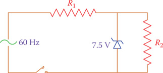
Figure P15.2 Circuit of Problem 5.
- In Problem 1, find the total current if the battery voltage drops to 11 V?
- Figure P15.2 shows a circuit whose source is AC. Plot the variation of the current in R2 for one cycle of the alternating current.