
18
Transistor Circuits
OBJECTIVES: After studying this chapter, you will be able to
- Describe the characteristic curves of transistors
- Explain other ways that a transistor amplifier can be made
- Define various classes of amplifiers and their differences
- Use transistors in circuits
- Use a transistor for voltage or current amplification
- Define emitter follower
- Explain the input and output impedances
- Explain impedance matching
- Define voltage and current gains
- Describe coupling in amplifiers and the ways this is carried out
New terms: Active region, breakdown voltage, cascaded, conduction angle, coupling (in amplifier), current gain, emitter follower, fixed bias, impedance matching, input impedance, load line (in transistor), output impedance, power gain, quiescent point, saturation, self-bias, swing, voltage gain
18.1 Introduction
In Chapter 17 we discussed how a transistor can be used as a switch and how it can amplify a signal. We also discussed the importance of correct biasing for transistors, in addition to many facts about transistors and their operation. There is still more to learn about transistors and their applications. One must have a good understanding of the contents of Chapter 17 before continuing with this chapter, where we discuss more about transistors and other ways that a transistor can be biased, as well as the three transistor configurations that are used for amplification. We also discuss the characteristic curves of transistors and various classes of amplifiers.
18.2 Transistor Characteristic Curves
A fundamental property of a transistor and how it works was pointed out in Figure 17.9, where a transistor is correctly biased by two power supplies. Although now we know how to use a single power supply to provide the necessary voltages for base current and collector current, here, for the sake of simplicity, we use the same figure with some modification for this discussion. Figure 18.1 shows a simple circuit of a transistor, in which the 1.5 V battery and the resistance RB determine the base current IB, and the 24 V battery together with RC define the collector current IC. We are interested in determining the variation of the collector current IC. This current can be varied either by changing the base current IB or the collector-emitter voltage VCE(the voltage between the collector C and the emitter E). See Figure 17.10. The base current can be varied by the variable resistor RB.
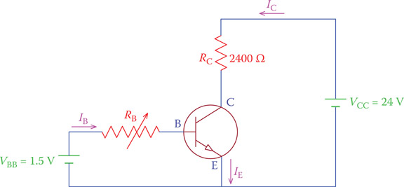
Figure 18.1
Simple circuit for a transistor operation.
The characteristic curves of a transistor provide the relationship between collector-emitter voltage and collector current for different values of the base current. Because there are two parameters that affect IC, a set of individual curves shown together denote various operating conditions. A typical curve is shown in Figure 18.2a, and a set of these curves are depicted in Figure 18.2b. Each individual curve depicts the variation of IC versus the value of collector-emitter voltage (VCE) for a fixed value of base current IB. When IB is zero, a transistor is cutoff, and it does not conduct no matter how much voltage is applied to the collector; any collector current is due to leaks, is very small, and is negligible. In both Figure 18.2a and b the curve corresponding to IB = 0 is exaggerated for clarity. The area under the curve corresponding to IB = 0, shaded in Figure 18.2a, represents the region where a transistor is cutoff and is not conducting.
For each nonzero value of IB the collector current starts from zero when the collector-emitter voltage is zero. A transistor starts conducting and the collector current increases rapidly when VCE > 0. The area around this abrupt change in IC, also shaded in Figure 18.2a, corresponds to when a transistor is in saturation. Saturation implies that the collector current has reached its maximum value for that collector-emitter voltage and cannot increase further by increasing the base current IB. For example, consider point M corresponding to VCE = VMin Figure 18.2b. For this point, IC has reached its maximum and cannot be increased by increasing IB. In contrast, an increase in IB can move point N to N′, both corresponding to a collector-emitter voltage VN.
Saturation (in a transistor): The state of a transistor at which the collector current has reached its maximum value for the present collector-emitter voltage, and cannot increase further by only increasing the base current IB.
The meaning of transistor saturation is better demonstrated in Figure 18.3, in which the scale of the horizontal axis is augmented, so that the line segments with sharp slopes can be better displayed. Two characteristic curves, corresponding to two base currents IB1 and IB2 are shown. Suppose that the collector-emitter voltage is 2 V. On both curves the corresponding point is A. This implies that if the base current is increased to IB2, but the VCE is still 2 V, the collector current does not change. The collector current increases only if the VCE increases, for instance, to 4 V, for which the operating point moves from A to B.

Figure 18.2
Collector current versus collector voltage characteristic curve of a transistor. (a) For one value of base current. (b) For multiple values of base current.
When saturated, a transistor cannot operate as expected. In normal operation, transistors function in the active region, the area that the characteristic curve is a segment of an almost horizontal straight line. In this region increasing collector-emitter voltage has little effect on the collector current. In other words, the transistor exhibits a large resistance in this region, so that increasing voltage has little effect on the current through it. This resistance is variable because it depends on the value of IB(for each value of IB the ratio VCE/IC is different).
Active region: An area in the characteristic curve of a transistor, in terms of collector–emitter voltage and collector current values that the transistor can function. If any of these values falls outside of its range a transistor falls in the saturation region or cutoff region and cannot function (see Figure 18.2a).
The active region is between the two voltages denoted by VA and VBR in Figure 18.2a. If VCE surpasses the breakdown voltage VBR, the transistor gets damaged, and if VCE < VA, the transistor is in saturation state.
Breakdown voltage: Voltage at which a semiconductor device changes behavior or gets damaged.
The operating point of a transistor is a point on these curves, corresponding to a given IB and a given value for VCE. A transistor, nevertheless, cannot work at all the possible points that can be found on the characteristic curves. This is because of the physical limitations of a transistor in handling a collector current without getting overheated and damaged. The limiting power boundary is shown in Figure 18.4 by the dashed curve for a typical transistor. It is possible to run the transistor in all the points to the left of the dashed curve, but not on the region on the right side of this curve. In this region, either IC is high or VCE is high, resulting in relative high power consumption in a transistor, which converts to heat.
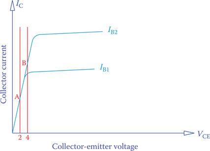
Figure 18.3
Typical set of characteristic curves for a transistor.
The operating point for a transistor (represented by Q in Figure 18.4) under the operating conditions governed by the supply voltage VCC and the base voltage VBB (see Figure 18.1) and the resistances RB and RC is at the intersection of lines corresponding to VCE and the base current. For a constant set of values for VCC, VBB, and RC if RB is varied the value of IB, and consequently IC and VCE, change. Each pair of IC and VCE defines an operating point denoted by Q. When as a result of varying RB, while the parameters VCC, VBB, and RC are kept constant, the values of the collector-emitter voltage VCE and collector current IC vary, this point Q moves on a straight line AB, as shown in Figure 18.4.
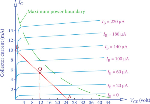
Figure 18.4
Operating point and boundary curve for the maximum power capacity of a transistor.
VCE is obtained from the supply voltage VCC minus the voltage drop in RC (and any other resistor in the collector-emitter loop connected to VCC, as we see later). In the cutoff state the current through RCis zero and no voltage is dropped in RC (and any other resistor in series with RC in the same loop). Consequently, all the applied voltage (VCC) appears at the collector. This defines point A of the line, where VCE is maximum. Also, if a transistor is conducting, but there is no internal resistance between C and E, this defines the maximum current that the collector can have (point B of the line). This maximum current can be found by dividing VCC by all the resistors in the loop (only RC in Figure 18.1). Thus, for a given supply voltage VCC the collector current can vary between zero (at point A) and a maximum value (at point B), as the line AB shows. The intersection of this line with one of the transistor characteristic curves defines the operating point Q. The line AB is called the load line. The load line, thus, represents all the possible locations of point Q for a transistor in a given circuit with constant VCC and resistance(s) in the collector-emitter circuit.
Load line (in transistor): Line showing the operating points of a transistor on a transistor characteristic curve, based on the supply voltage and the resistors in the transistor circuit. This line is between the points corresponding to the maximum collector voltage and maximum collector current.
Example 18.1
For the transistor shown in Figure 18.1, whose characteristic curves are shown in Figure 18.4, if the base current is 60 μA, find the collector current and the value of ß.
Solution
The maximum current through the collector is defined by dividing the supply voltage (24 V) by the resistor RC. Thus, point B end of the load line on the current (vertical) axis is at
24 ÷ 2400 = 0.01 A = 10 mA
The other end of the load line (point A) is on the horizontal axis at 24 V. This line is the same as shown in Figure 18.4 and intersects the curve corresponding to 60 μA base current at point Q (as shown). Dropping a perpendicular from Q to the vertical axis gives the current in the collector. On the basis of the figure this current is 5.5 mA.
The value for ß can be found from dividing collector current by the base current.
5.5 mA ÷ 60 μA = 5500 μA ÷ 60 μA = 91.67 ≈ 92
Example 18.2
If in Example 18.1 the supply voltage changes to 30 V and RC is 2200 Ω (other parameters remaining unchanged), how much are IC and VCE?
Solution
A new load line needs to be drawn on the same graph of Figure 18.4. The intersection of this line with the line corresponding to IB = 60 μA defines the values of IC and VCE.
Point A for this new line is at VCE = 30 V, thus between 28 and 32 (not shown), and point B is at IB = 30 ÷ 2200 = > 13.6 mA. If you draw this line you will find its intersection with 60 μA base current, which corresponds to IC = 5.6 mA and VCE = 17.4 V.
18.3 Common-Emitter Amplifier
As explained in Section 17.5 and depicted in Figure 17.8, there are three modes of operation of transistors: common emitter, common base, and common collector. Consequently, there are three ways a transistor can be employed as an amplifier, and, therefore, we have three categories of amplifiers: common-emitter amplifier, common-base amplifier, and common-collector amplifier.
In each category the common element of a transistor is shared between the input and the output. The example we studied in Chapter 17 had the structure of a common-emitter amplifier, because the emitter was grounded, the input was introduced between the base and ground, and the output was taken from the collector. Nevertheless, the load was not connected to the points where normally is considered for the output. This implies that in electronics designs there are always different ways to perform the same function.
A common-emitter amplifier is the most widely used category among the three. Figure 18.5 illustrates a common-emitter amplifier. In this figure, as seen before, for biasing the transistor and supplying the base with a suitable voltage, use is made of a voltage divider between the supply voltage and the ground. Moreover, as pointed out in Chapter 17 (see Section 17.11 and Figure 17.23), RE is added to adjust the base current, as opposed to RB in Figure 18.1. The input is introduced between the base and ground, and the output is taken between the collector and ground. The output voltage is equal to VCE plus the voltage drop in RE. Notice the phase relationship between the input and the output. They are 180° out of phase.
In practice, instead of the circuit in Figure 18.5a, the circuit in Figure 18.5b is used, in which CE is added. In this circuit RE adjusts the voltage at E as necessary. The role of the bypass capacitor CE is to provide a ground at the emitter for AC signals. In this way the voltage at the emitter is pure DC (without variation) particularly at higher frequencies for which the reactance of CE is small and acts as a short to ground (for AC signals).
In ordinary applications the resistor RE is normally chosen such that the voltage across it is around one volt. Note that because RE is in the emitter circuit the voltage across it determines the emitter current IE. Also, because IB is normally very small, the biasing voltage can be selected by noting that it must compensate for the voltage drop in RE and the drop across the BE junction. In practice, a good value for RE is around 10 percent of RC.
In a common-emitter amplifier the input and the output signals are 180° out of phase.

Figure 18.5
Schematic of a common-emitter amplifier. (a) Typical resistance values for a general application transistor. (b) Capacitor CE is added to emitter to provide a zero ground for AC signals.
Example 18.3
Draw the load line for the transistor amplifier circuit shown in Figure 18.6a. If the operating point Q is in the middle of the load line, find IC, VCE, and the voltage at the emitter.
Solution
The load line is shown in Figure 18.6b. The point corresponding to the maximum VCE is at 25 V, and the value of maximum IC, defining the other end of the load line is
| IC-max=252200+200=0.0104 A=10.4 mA |
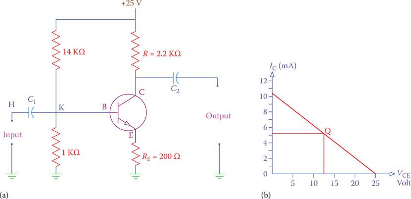
Figure 18.6
(a) Transistor circuit and (b) the load line, for Example 18.3.
At the midpoint of the load line values of both IC, VCE are half of the maximum values. Thus, IC= 5.2 mA and VCE = 12.5 V. Because IE ≈ IC we can say with good approximation that the emitter voltage is equal to the voltage drop in the 200 Ω resistor. Thus,
VE ≈ (200)(5.2) ÷ 1000 = 1.04 V
We have already seen how a transistor can be biased. At this point we introduce two more ways that the transistor in Figure 18.5 can be biased. These are shown in Figure 18.7a and b. Notice that the emphasis is on the biasing methods. Observe the difference between the three ways of biasing, by comparing Figures 18.5a, 18.7a, and b. All of these alternatives are used in practice. The terms used for distinguishing between the various ways of biasing as shown are fixed bias for Figure 18.7a and self-bias for Figure 18.7b. The amplifier in Figure 18.5 is voltage divider biased. In a fixed bias configuration the voltage at point K is a fixed value, determined by the supply voltage and the resistors involved. In a self-bias configuration the voltage at K is not fixed, but it is of the correct polarity to forward bias the base-emitter junction.
Fixed bias: Type of biasing in a transistor in which a fixed resistor is connected between the base terminal and the power supply, thus providing a fixed voltage at the base.
Self-bias: Type of biasing in a transistor in which a fixed resistor is connected between the base terminal and the connector, thus providing a voltage at the base that varies with the current through the collector.
18.4 Common-Base Amplifier
In the same way that we have seen for a common-emitter amplifier so far, it is possible to use a transistor with common-base configuration for amplification purposes. The conditions for correct biasing do not change. Only the base must be common between the input and the output. Figure 18.8 illustrates a typical case for a common-base amplifier. As you recall, the base-emitter junction must be forward biased; thus, the base voltage for an NPN transistor must be higher than the emitter voltage. In this respect, if the base is at zero voltage, the emitter voltage needs to be negative. In such a case, a power supply with both positive and negative polarity, similar to that depicted in Figure 16.17 (see Section 16.7) may be utilized to provide the necessary biasing voltages.
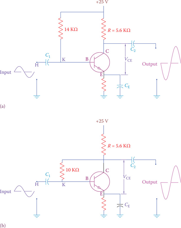
Figure 18.7
Common-emitter amplifiers with (a) fixed bias and (b) self-bias.
To avoid the necessity for two power supplies, the base can be biased by one of the alternative methods so that it is still forward biased while the emitter voltage is raised to zero. This is shown in Figure 18.8b.
As also shown in Figure 18.8, for a sinusoidal input the output signal is in phase with the input signal. This is a characteristic of the common-base amplifier. For a common-base amplifier the characteristic curves define the variation of collector-emitter voltage versus collector current for various emitter currents. In the active region the collector current stays constant no matter how much VCE changes (this is obvious, because IC ≈ IE). This fact is reflected in the curves shown in Figure 18.9, each of which is almost a horizontal line segment.

Figure 18.8
Schematic of a common-base amplifier. (a) Base is directly grounded (zero voltage), or (b) it can have a DC voltage (a capacitor is required), then emitter can be at zero voltage.
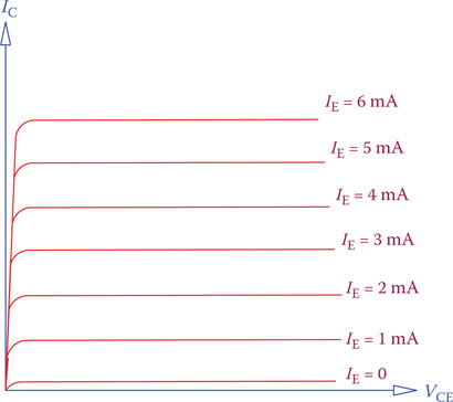
Figure 18.9
Characteristic curves for a common-base amplifier.
In a common-base amplifier the input and output signals are in phase.
18.5 Common-Collector Amplifier
In a common-collector amplifier, as the name implies, the collector is common between the input and the output; thus, the input signal is introduced between the base and the collector, and the output signal is taken between the emitter and the collector.
Figure 18.10 illustrates the schematics of a common-collector amplifier. The collector has no resistance attached to it and is grounded through a capacitor C2. The role of the capacitor C2 is to block the DC voltage of the power supply from ground. Otherwise, the supply is directly grounded. In the configuration shown, thus, the input is applied between the base and ground, and the output is taken from the emitter and ground. The roles of the capacitors C1 and C3 are, again, to isolate DC voltages and signals from being transferred from the input to the base and reaching to the output (see Section 17.10).
A characteristic of the common-collector amplifier is that the output signal is in phase with the input signal, as shown in Figure 18.10. Also, for this configuration the output current is IE, which is much larger than the input current IB. In fact, a common-collector amplifier is used for amplifying current because the output current is a direct amplified value of the input current. That is, the output obtained from the emitter is following the pattern of the input to the base, but with a higher current capability. For this reason the common-collector amplifier is called an emitter follower (emitter follows the input).
Emitter follower: Name given to common collector amplifier.
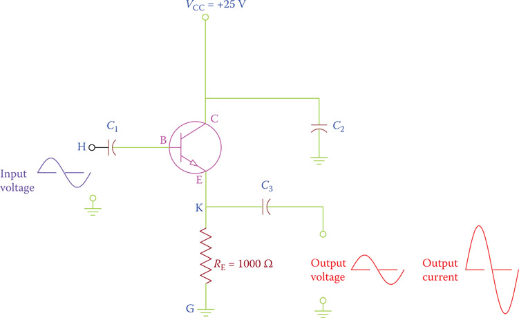
Figure 18.10
Schematics of a common-collector amplifier (emitter follower).
Another characteristic of the common-collector amplifier is that the output voltage is (slightly) smaller than the input voltage. This can be seen from the voltage relationships between the points H and G (the ground),
and K and G in Figure 18.10 (VHG > VKG, considering the voltage drop between B and E junction in the transistor).
18.6 Current Gain, Voltage Gain, and Power Gain in Amplifiers
From the study of amplifiers it can be seen that in an amplifier a transistor is governed by the input signal and generates an output signal that (1) has the same frequency as the input and (2) its voltage or its current capacity (or both) are several times larger than those of the input signal.
In practice, on the basis of the requirement, the voltage of a signal, the current of a signal or both must be amplified. If both the current and the voltage need to be amplified, two or more amplifiers must be cascaded together when at least one is for voltage amplification and one is for current amplification (see Section 18.9).
The quantitative amplification of current and voltage are called current gain and voltage gain, respectively. They represent the ratio of output current (voltage) variation to the value of the input current (voltage) variation. The term swing is employed to refer to the total variation of voltage or current. Because in most applications the input signal is not DC, it is standard practice to consider a sinusoidal waveform to study the characteristics and gains of an amplifier. In this respect, the current gain and voltage gain can be measured by the ratio of the peak-to-peak value of the sinusoidal output signal (output swing) to the peak-to-peak value of the sinusoidal input signal (input swing).
Current gain: Ratio of the output current variation to the input current variation in an amplifier.
Voltage gain: Ratio of output voltage variation (output swing) to the input voltage variation (input swing) in an amplifier.
Swing: Total change (the difference between the maximum and minimum values) of the input or the output in an amplifier.
In addition to the current gain and voltage gain, we also have power gain. Power gain determines how much the output power is larger than the input power. Because power is the product of voltage and current, power gain is determined from multiplication of current gain and voltage gain.
Power gain: Ratio of output power to the input power in an amplifier.
An amplifier current gain, voltage gain and power gain are denoted by AC, AV, and AP, respectively. The following relationships summarize the definitions for the three gain values in amplifiers. The Greek capital letter Δ (delta) is employed to represent the total change or swing. For an AC signal the total change is the peak-to-peak value.
| Current gain (AC)=△Iout△Iin | (18.1) |
| Voltage gain (AV)=△Vout△Vin | (18.2) |
| Power gain (AP)=AC×AV | (18.3) |
Table 18.1 Characteristics Summary of the Three Types of Amplifiers
| Common Emitter | Common Base | Common Collector | |
| Current gain | Normal | Less than 1 | Normal |
| Voltage gain | Normal | Normal | Less than 1 |
| Phase relationship (input-output) | 180° out of phase | In phase | In phase |
As we have seen so far, the three types of amplifiers have different characteristics. Table 18.1 summarizes the properties of these single amplifiers. The word normal is used to refer to a practically acceptable value for amplification.
Example 18.4
Referring to the amplifier whose characteristic curves are shown in Figure 18.11, the output is taken from the collector. If the input voltage variation is between 40 and 160 mV and the output voltage changes between points M and N, as shown, how much is the amplifier voltage gain.
Solution

Figure 18.11
Relative positions of DC and AC load lines.
The output has a swing of 14.6 V − 6.8 V = 7.8 V, and the input has a swing of 0.160 V − 0.040 V = 0.120 V. The voltage gain, thus, is
| Voltage gain =7.80.12=65 |
18.7 Amplifier Classes
Transistors are widely used in radio, TV, sound recording and play back, communications, and so on. In practice, often a few single transistor amplifiers are cascaded together in order to obtain a desired level of amplification of voltage and power. The discussion about specific application of amplifiers is outside the scope of this book. Thus, the discussion below is for single transistor amplifiers.
There are a number of classes of amplifiers, but four of them are more common. These are classes A, B, C, and AB. Before we discuss the difference between them and the reason why they are needed, we study the effect of biasing a transistor when its input is an AC signal. As usual, we consider a sinusoidal waveform as the signal to be amplified. This is a reinforcing of what we have already seen along the discussions in Sections 17.10 and 17.11.
Consider a common-emitter (CE) amplifier, as shown in Figure 18.5. We have already defined the load line and what it implies. First, without going into details, there are two load lines for a transistor, one corresponding to DC operation and one corresponding to AC operation, called AC load line. The AC load line is for when the input signal is AC and varies; the DC load line is for the case that the input signal has not much rapid change and can be considered to be DC. For a given Q point of a transistor in a circuit the position of the AC load line has a slight clockwise rotation about point Q with respect to the DC load line, as shown in Figure 18.11. Line AB in this figure represents the DC load line and line A′B′ is the AC load line.
Point Q, thus far referred to as operating point, is called the quiescent point, because it determines the “no signal” condition of a transistor. This point is defined by the bias condition of the base (assumed CE amplifier) governed by the resistances used in the circuit, the internal resistances of a transistor and the supply voltage. In other words, if there is no input to the transistor the collector current (IC) and the collector-emitter voltage (VCE) are those corresponding to point Q. In Figure 18.11 this point corresponds to IC = 5.3 mA. Now, suppose that the input signal is sinusoidal and causes the collector current change between 3.3 and 7.3 mA. This causes the operating point of the transistor to move on the AC load line between points M and N (see Figure 18.11) and generates a sinusoidal output signal whose peak-to-peak value is between 6.8 and 14.6 V, as depicted in Figure 18.11. As far as M and N are on the line A′B′ and do not pass over the two ends of this line segment, the transistor can amplify the input signal and reproduce a complete sinusoidal signal at its output.
Quiescent point: Point on the load line of a transistor in a circuit. This point corresponds to a condition that the circuit input does not change (stays quiescent).
Figure 18.12 shows a similar representation to that depicted in Figure 18.11. The characteristic curves and the DC load line have been removed for clarity, and only the AC load line is shown. The biasing condition leads to a quiescent point Q, almost in the middle of the load line. Suppose now that a sinusoidal input signal is introduce at the amplifier base. When blended with DC bias voltage, it causes the base current to swing between 20 and 180 μA; that is, a swing of 160 μA. This causes the operating point of the transistor to travel along the load line. The variation of the sinusoidal input signal causes the collector current to assume values between 2 and 6 mA. In other words, the collector current has a swing of 4 mA. Consequently, the collector-emitter voltage has a swing of 20 V (between 10 and 30 V), as depicted in Figure 18.12. For the operating condition shown, an input signal with larger peak-to-peak values leads to a larger swing in the base current, and consequently, a larger variation in the collector current. Nevertheless, the maximum allowable collector current swing is between 0 and 8 mA. Any larger signal that forces the collector current beyond its extremities causes the transistor either to cutoff or to saturate. In both these conditions a transistor cannot perform as expected.

Figure 18.12
Effect of an AC input on the transistor collector values.
Figure 18.13 depicts the same transistor with three different bias conditions. Figure 18.13a is the same as Figure 18.12 except that the input signal representation is removed. It is repeated for ease of comparison with Figure 18.13b and c. We want to draw attention to the important fact that if the quiescent point Q is not in the middle, even the signal that causes a 4 mA swing in the collector current can run the transistor into cutoff or an unfeasible condition. As a result, for those values that the transistor can function it produces an output with the proper voltage, and for those values outside the operational conditions, it does not function. The outcome, consequently, is an incomplete or truncated output, as shown in Figure 18.13b and c. The same conclusion was shown in a different way in the discussion in of Chapter 17 (Section 17.11).

Figure 18.13
Controlling output through selecting the quiescent point Q by transistor bias. (a) No clipping. (b) Negative side is clipped. (c) Positive side is clipped.
The operating conditions depicted in Figure 18.13b and c are not necessarily useless or unwanted. In fact, from certain viewpoints they are desirable. For instance, a transistor is not conducting 100 percent of the time, and it finds time to cool off in each cycle when it is in the cutoff state. The amplifier classes stem from the operating bias condition (initial positioning of point Q). There are more than four classes of amplifiers, but four of them are more common, as described below.
Class A Amplifier
A class A amplifier amplifies the entire input signal in the same manner as we have already seen in Figures 17.19 and 18.12. This is through biasing a transistor in such a way that the range of voltages in the signal never run the transistor into cutoff. This implies that the transistor is always conducting, and, therefore, a good portion of the power consumed is converted to heat in the circuit components and the transistor, itself.
Class B Amplifier
A class B amplifier amplifies only 50 percent of the input signal; thus, operating only 50 percent of the time, just in the same way that we have already seen in Table 17.2 and Figure 17.22. This is done, as seen before, by proper biasing of the transistor to operate only for one half, either the positive parts or the negative parts, of the input. When amplification of the whole input signal is desired, two amplifiers are used back to back; each one acts only on half of the input signal. Then the two halves are put together (the two transistors are normally of two different types for this application; one is PNP and the other is NPN). The advantage of such an arrangement is that each transistor works only for half of the time and is cutoff for the other half. In this way the heat generated is less than in a class A amplifier, and higher power can be handled. A class B amplifier, thus, has a better efficiency than class A.
Class AB Amplifier
Although from an efficiency viewpoint a class B amplifier is preferred to class A, it suffers from introducing some degree of distortion to a signal, which is not acceptable in many cases, such as for sound and video signals. A third class, which overcomes this drawback of class B is class AB amplifier. Class AB has the same structure as class B, with slight modification, so that it operates at more than 50 percent of time (clips the output by less than 50 percent). This improves the performance when used in pairs.
Class C Amplifier
A class C amplifier has a bias such that more than 50 percent of the input signal is clipped, and the rest appears in the output. There are many applications for which class C amplifier is sufficiently acceptable or even more appropriate. The energy loss of class C amplifier is, therefore, less than that of class B.
Conduction angle:
The same as “angle of flow.”
Angle of flow: Measure of percentage of time (based on 100 percent for 360°) for one cycle of a sinusoidal waveform during which an amplifier is in an operating state (transistor is conducting in a transistor amplifier.)
To define the performance of an amplifer with respect to its class of operation, a term conduction angle (or angle of flow) is employed. The coduction angle defines what percentage of a signal is amplified. Using a sinusoidal signal, 100 percent corresponds to 360° conduction angle, and 50 percent corresponds to a conduction angle of 180°. In this sense, class A and class B amplfiers have conduction angles of 360° and 180°, respectively. Accordingly, the condution angles of class AB and class C amplifers are more than 180° and less than 180°, respectively. The output of the four classes of amplifiers to a sinusoidal input is shown in Figure 18.14.
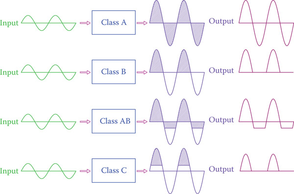
Figure 18.14
Input-output relationship of four classes of amplifiers.
Comparing the above four classes of amplifiers, it can be seen that the initial position of the quiescent point Q on the load line determines the class. The amplitude of the input signal (input swing) comes into consideration for class A, AB, and C. For class B, point Q must be at either of the two ends of the AC load line.
18.8 Input and Output Impedance
In all amplifiers, there is an input signal from an outside source that is connected to the amplifier input, which is amplified and delivered to an output device. For instance, in a wind turbine the wind speed is measured by a type of sensor. The measurement value will be in the form of a voltage or current that varies with change in the wind speed. If this signal is small, it needs to be amplified before being processed for integration in the turbine control software. Examples of this nature are plenty in industry. Normally, when there is a measurement of any varying parameter, the measured signal needs amplification.
The discussion here is not specific to an amplifier. It is true for many devices with an input or/and an output. We refer to an amplifier as a good example because so far we have gained some knowledge about them.
Figure 18.15a illustrates the schematics for the input and output connection to an amplifier. The amplifier is connected to the input device through point terminals A and B and to the output device through points
For maximum power transfer the impedances of two devices that are to be connected must be equal to each other.
C and D. Because an amplifier has various components, its effect on any external device makes it look as if that device is connected to a circuit consisting of resistors, inductors, and capacitors, having a measureable impedance value. That is, the amplifier appears as an impedance to the external device and exhibits some impedance value toward the circuit of that device, as shown in Figure 18.15b.

Figure 18.15
Definition of input and output impedances. (a) Amplifier with its input and output connections. (b) Amplifier circuit as seen from the outside device.
The input impedance is the value of impedance an amplifier exhibits to its input device, and the output impedance is the value of impedance an amplifier exhibits to its output device. These values are specific to an amplifier and are independent of the external devices. When connecting to an external device, the input and output impedances of an amplifier are in series with the impedance of that external device. In this respect, the voltage that arrives to the amplifier input, or is delivered to the output device, is determined from the voltage divider that is formed this way. This is schematically shown in Figure 18.16.
Input impedance: Value of impedance an amplifier (or a circuit, in general) exhibits to its input device, so that the device sees the amplifier as an impedance of that value.
Output impedance: Equivalent impedance an electronic device (such as an amplifier) exhibits to the device connected to its output.
From a practical viewpoint the values of input impedance (Zin) and output impedance (Zout) are very important. The importance is in matching the impedance values between each two devices that must be connected together. In the same way that an amplifier exhibits impedance to the input and output devices, the input and output devices exhibit impedance to the amplifier. This is true, indeed, for any two devices that must be connected together. For maximum power transfer between two devices that are to be connected their impedances must be equal. If they are not exactly the same, their values must not be too much different. If instead of maximum power transfer, some other criterion is more important, for instance, for maximum voltage gain, then this rule does not need to be enforced.
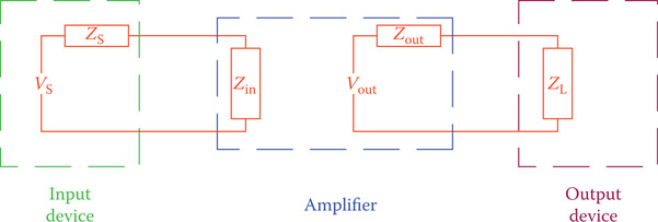
Figure 18.16
Input (output) impedance is in series with the external device impedance.
18.9 Coupling and Impedance Matching
In many electronic applications in which a signal must be amplified, it becomes necessary to carry out this process in a number of stages and through more than one amplifier. In such applications a number of single amplifiers, as we have seen so far, are put in series with each other. This means that the output from the first amplifier serves as the input for the second, and the output from the second amplifier is the input for the third, and so forth. The amplifiers are said to be cascaded together, and each amplifier constitutes a stage of amplification.
Cascaded: Way of putting devices of the same functionality together in succession to each other for enhancing their effect, such that the output from one is the input to the next, like two or more amplifiers.
The last stage is normally a power amplifier (amplifying current). For example, if there are only two amplifiers, the first one is a voltage amplifier and the second one is a current amplifier (and not the reverse). When two or more single amplifiers are cascaded together, the final gain of the system is obtained by multiplying the gains of the individual stages. For instance, for a three stage amplifier the final power gain is
| AP=(AP)1(AP)2(AP)3 | (18.4) |
where APstands for power gain, and the subscripts 1, 2, and 3 refer to the power gain for each stage.
Connecting the output of each amplifier to the next stage is called coupling. For efficient working of the set of amplifiers in cascade it is important that their impedances are appropriate for connecting together. In other words, they must match together. For example, if maximum power transfer is concerned, the mating impedances must be equal. Other objectives may require other conditions. This is called impedance matching. It is also true for the first and the last stages that connect to external devices. The output impedance of an input device must match the input impedance of an amplifier. Similarly, the input impedance of an output device must match the output impedance of an amplifier.
Coupling (in amplifier): Act of properly connecting an amplifier to its input or output or connecting two amplifiers in cascade.
Impedance matching: Selecting suitable values for resistors, capacitors and/or other components so that the output from one device matches the input of the following device for a desired purpose such as maximum power transfer or other criteria.
There are a number of coupling methods. These are direct coupling, RC coupling, LC coupling (or impedance coupling), and transformer coupling.
In a direct coupling the output of one stage is directly connected to the input of the next stage. This is shown in Figure 18.17, where two NPN common-emitter amplifiers are directly coupled together. In Figure 18.17 the only connection between the two transistor amplifiers is by the line MN.
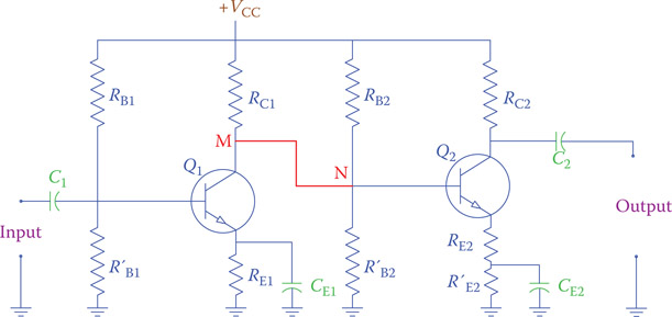
Figure 18.17
Direct coupling between transistors Q1 and Q2.
Figure 18.18 illustrates an RC coupling or (resistive-capacitive coupling). This circuit is exactly the same as in Figure 18.17 with the exception that a capacitor has been replaced for the line MN. In this configuration the only link between the two transistors is the capacitor C.
A third type of coupling is obtained if in Figure 18.18 the resistor RC1 is replaced by an appropriate inductor. Such an arrangement is called impedance coupling. This circuit is not shown because it is similar to that in Figure 18.18 except the inductor replacing the collector resistance of transistor Q1. In operation, this circuit is sensitive to frequency. For higher-frequency applications this circuit is preferred to the previous ones.

Figure 18.18
RC coupling between two common-emitter amplifiers.
Finally, one version of a transformer-coupled two-stage amplifier is shown in Figure 18.19 (there are other alternative ways for this). Using a transformer has the advantage of impedance matching as well as increasing the efficiency of a system by replacing resistors that consume electricity and convert it to heat. It also allows the inversion of polarity of the output signal, if required. Impedance matching is very important, as mentioned before, and it is very common to achieve this by using transformer coupling. The relationships between the current, voltage, and power of the primary and secondary circuits work here for appropriate selection of a desirable transformer. The frequency range of signals must also be brought into consideration because this type of coupling is also sensitive to frequency.
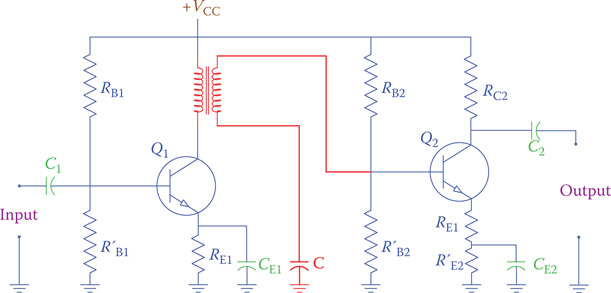
Figure 18.19
Transformer coupling.
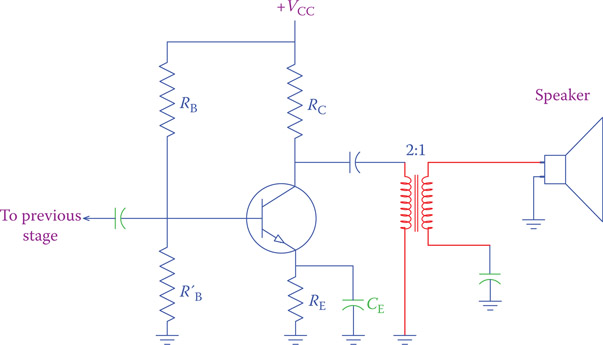
Figure 18.20
Impedance matching for the speaker of an audio system.
A common example of impedance matching by a transformer takes place in many audio devices. The input impedance of many loudspeakers is 8 Ω, but some come with 4 or 16 Ω. If the output impedance of the last stage of the audio device, usually, a power amplifier (amplifying current), is 16 Ω then there is a mismatch if a 4 Ω speaker or an 8 Ω speaker is connected to it. By transformer coupling this mismatch can be corrected, as seen in Figure 18.20. Example 18.5 is a simple case showing the effect of a mismatch.
Example 18.5
Consider a 50 W (nominal) amplifier that requires a 4 Ω speaker to deliver about 50 W at its output. What happens if you connect an 8 Ω speaker to this amplifier?
Solution
The impedance of a speaker normally reflects its impedance as a result of the coil resistance and its inductive reactance at the standard frequency of 1000 Hz. From Ohm’s laws and simple calculations (just using the relationships between voltage, current, and power, and considering the speaker as a resistance) we may conclude that the voltage provided by the amplifier at its terminal to connect to a speaker is
| V=√PR=√(50)(4)≈14 V |
If a 4 Ω speaker is connected to this amplifier, the current in the speaker coil is
| I=144=3.5 A |
and the product of voltage and current is about 50 W.
Now, if instead of a 4 Ω speaker an 8 Ω speaker is connected the current is half of the previous value and the power delivered by the speaker (product of voltage and current) is only about 25 W. Thus, the amplifier is underutilized and is not delivering its full power.
Suppose now that the speaker is connected to the amplifier through a small audio transformer of 1:1.5 ratio. The transformer increases the voltage by the ratio of 1.5 to 21 V.
The new current in the speaker is
| INew=218=2.625 A |
and the power drawn by the speaker is
PowerNew = (21)(2.6) = 55 W
This new power is more like what one expects from this amplifier. The more precise ratio for 50 W power delivery is 1:1.4 (or more precisely √2), but purposely we selected 1:1.5 for this discussion.
18.10 Testing Transistors
A transistor can be tested to see if it is good or faulty. An ohmmeter, analog or digital, can be used for this purpose. If a digital multimeter is employed, the check diode may be used. The resistance between each two terminals (base, collector, and emitter) should be checked. Because a transistor is made of two junctions, the same thing that was mentioned about diodes is valid here, too. The forward bias resistance must be low, and the reverse bias resistance must be very high (OL in a digital meter).
Remember that in an NPN transistor the base-emitter junction is forward biased if the base is connected to + and emitter is connected to −; similarly, the base-collector junction is forward biased if the base is connected to positive and the collector is connected to −. The positive lead of a meter is always red, and the negative lead is always black. The expected meter reading for an NPN transistor is, thus, as shown in Table 18.2. The numerical values shown in the table correspond to when the check diode option of a meter is used.
Table 18.2 Summary of Ohmmeter Reading for an NPN Transistor
| Terminals |
Connections
|
Meter Reading | |
| Emitter−base | Base to + (red) | Emitter to−(black) | 0.4–0.7 |
| Base to−(black) | Emitter to + (red) | Very high (OL) | |
| Collector−base | Base to + (red) | Collector to−(black) | 0.4–0.7 |
| Base to−(black) | Collector to + (red) | Very high (OL) | |
| Collector−emitter | Collector to + (red) | Emitter to−(black) | Very high (OL) |
| Collector to−(black) | Emitter to + (red) | Very high (OL) | |
Table 18.3 Summary of Ohmmeter Reading for a PNP Transistor
| Terminals |
Connections
|
Meter Reading | |
| Emitter-base | Base to + (red) | Emitter to−(black) | Very high (OL) |
| Base to−(black) | Emitter to + (red) | 0.4–0.7 | |
| Collector-base | Base to + (red) | Collector to−(black) | Very high (OL) |
| Base to−(black) | Collector to + (red) | 0.4–0.7 | |
| Collector-emitter | Collector to + (red) | Emitter to−(black) | Very high (OL) |
| Collector to−(black) | Emitter to + (red) | Very high (OL) | |
Because a PNP transistor has an opposite structure, the directions of forward and reverse bias invert. Table 18.3 shows a summary of the meter reading for such a transistor. In each case if the readings are different, then the tested transistor is faulty.
18.11 Chapter Summary
- Each transistor has a set of characteristic curves.
- Characteristic curves represent the variation of the collector current versus the collector-emitter voltage.
- Characteristic curves also show the saturation and cutoff regions for a transistor.
- Saturation is a state that a transistor’s collector current has reached its maximum value for a given base current and cannot go higher unless the collector-emitter voltage is increased.
- Cutoff is a state that a transistor does not conduct, and there is no collector current (the current between collector and emitter is zero).
- A load line of a transistor is a straight line connecting the point for maximum collector-emitter voltage to the point with maximum collector current, for a given VCC, RC, and RE.
- If the voltage applied to the collector of a transistor is so high that VCE exceeds the breakdown voltage, the transistor gets damaged.
- There are a number of ways to bias a transistor. Among these are self-bias, fixed bias, and voltage divider bias.
- The quiescent point is the operating point of a transistor (on its load line) corresponding to no input.
- In a common-emitter amplifier the input is applied between the base and ground and the output is taken between the collector and ground.
- In a common-emitter amplifier the output is 180° out of phase with the input.
- A common-emitter amplifier is the most commonly used amplifier.
- In a common-base amplifier the input is applied between the emitter and ground and the output is taken between the collector and ground (base is grounded).
- In a common-base amplifier the output is in phase with the input.
- In a common-collector amplifier the input is applied between the base and ground and the output is taken between the emitter and ground. The collector is grounded through a capacitor or it may not be grounded.
- In a common-collector amplifier the output is in phase with the input.
- A common-collector amplifier is called an emitter follower because the emitter follows the input signal variation.
- In an amplifier, voltage gain is the ratio of the output voltage variation range (peak to peak if sinusoidal) to the input voltage variation range.
- In an amplifier, the variation range for a voltage or current is called swing.
- In an amplifier, current gain is the ratio of the output current swing to the input current swing.
- In an amplifier, the power gain is obtained by multiplying voltage gain by current gain.
- In an amplifier, conduction angle or angle of flow defines what percentage of each cycle of a sinusoidal input waveform is amplified and appears at the output.
- In a class A amplifier the whole cycle of an AC input signal is amplified. The angle of flow is 360°.
- In a class B amplifier, only one half cycle of an AC input signal is amplified. The angle of flow is 180°.
- In a class AB amplifier, more than one half cycle of an AC input signal is amplified. The angle of flow is between 180° and 360°.
- In a class C amplifier, less than half cycle of an AC input signal is amplified. The angle of flow is less than 180°.
- When two devices are connected together, each one sees the other as an impedance.
- The input impedance of an amplifier is the impedance value that an input device is subjected to when connected to the amplifier.
- The output impedance of an amplifier is the impedance value that an output device is subjected to when connected to the amplifier.
- Cascaded amplifiers are a number of amplifiers in series with each other, so that the output of each is the input for the next one.
- Impedance matching is necessary for efficient functioning of two devices that are connected together.
- Coupling implies how the electronic devices are connected together. Coupling can be direct, through a capacitor and resistor (RC coupling), through an inductor and capacitor (impedance coupling) or through a transformer.
Review Questions
- What are the characteristic curves of transistors?
- What is meant by saturation? Where is the saturation region on the characteristic curve graph?
- What is meant by cutoff?
- How many configurations of transistor amplifier do exist?
- What is the main difference when a common-emitter amplifier is compared to other amplifier configurations?
- In a common-emitter amplifier where are the input and output connections?
- What is the difference between class A and class B amplifiers?
- What is the difference between class B and class AB amplifiers?
- What is conduction angle?
- What is meant by swing?
- What is amplified in an amplifier?
- What is amplified in a power amplifier?
- What is the difference between voltage gain and current gain?
- What type of amplifier has a voltage gain less than 1?
- What is the load line? Is there any difference between load lines for DC and for AC?
- Which amplifier type is the most commonly used?
- What is an emitter follower?
- What is the difference between input and output impedances in an amplifier?
- Is impedance matching important? Why or why not?
- Name two types of coupling in amplifiers and other electronic devices.
Problems
- Refer to Figure 18.12. If this graph corresponds to a common-emitter amplifier, from the given data in the figure, find the current gain of this amplifier.
- In an amplifier the sinusoidal input voltage has a swing of 5 mV, while the peak-to-peak current variation is 48 μA. The output voltage has a swing of 40 mV, and the output current variation is between a minimum of 0.1 mA to a maximum of 0.7 mA. Find the power gain for this amplifier.
- Referring to Figure 18.11, consider the AC load line. In the current position of point Q the amplifier works as class A. Where is/are the possible point(s) for point Q so that the amplifier becomes class B?
- In Figure P18.1, if the collector current has a minimum of 1 mA and a maximum of 4 mA, what are the minimum and maximum values for collector-emitter voltage?
- In the amplifier of Problem 4, if the input is sinusoidal, what is the peak value of the output signal?

Figure P18.1
Circuit for Problem 4.