
17
Transistor
OBJECTIVES: After studying this chapter, you will be able to
- Explain what a transistor is and how it works
- Describe the structure of a transistor
- Define PNP and NPN transistors
- Recognize various transistors of different physical shapes
- Name the three elements of a transistor
- Explain the terms, common base, common collector, and common emitter
- Explain the two primary functions of a transistor
- Define what biasing a transistor is
- Describe bias conditions for a transistor to work
- Define cutoff state of a transistor
- Explain how a transistor can be used for switching
- Explain how a transistor can be used for amplification
- Understand the importance of correct biasing
- Describe heat sink
New terms: Base, biasing a transistor, bipolar junction transistor, collector, common base, common collector, common emitter, cutoff, emitter, heat sink, junction transistor
17.1 Introduction
A transistor is a semiconductor device with many applications. It is, in fact, the mother of all the other semiconductor electronic devices that we use or see around us today. Before transistors were invented, all electronic devices were made with vacuum tubes. Still one can find devices such as stereo amplifiers and radio receivers that use vacuum tubes, but they are rare and expensive, in addition to being bulky and heavy in comparison to solid-state electronics that use transistors and semiconductor technology. There are various types of transistors, and we will study their fundamentals in this chapter. The simplest form of transistor is a junction transistor, also called bipolar junction transistor. The reason for calling it junction transistor is because it contains two PN junctions. In other words, from the structure viewpoint it is similar to two diodes put together during the manufacturing process. Nonetheless, note that a transistor is a completely different device than a diode, meaning that one cannot put two diodes together and expect to have a transistor.
Junction transistor: Same as bipolar junction transistor, which includes any ordinary transistor.
Bipolar junction transistor: Another name for junction transistor.
17.2 Junction Transistor
Recalling that a PN junction has a P side and an N side, imagine you want to put two of them together. It is easy to understand that depending on how they are put together, two basic types of transistors can result, as shown in Figure 17.1.
Accordingly, the two types of a junction transistor are PNP and NPN. This classification is based on the polarity in the structure. There are other types of classification, based on transistor functioning and performance in a circuit.
As can be easily understood from Figure 17.1, a transistor has three terminals. This is different from the DC components that we have studied so far. In a transistor, irrespective of the type (PNP or NPN), the middle terminal is called the base. The other two terminals are called the emitter and the collector. The internal structure of a transistor and the amount of doping in each P and N material (which determine the thickness of the depletion region in a PN junction) determine which side is the emitter and which is the collector. The emitter junction is much higher doped than the collector junction. Figure 17.2 shows the symbols for junction transistors, where B, C, and E identify the base, emitter, and collector, respectively.
Base: One of the three principal terminals of a junction transistor (ordinary transistor).
Emitter: One of the three main terminals of a common (not FET) transistor.
Collector: One of the three main terminals of an ordinary transistor.

Figure 17.1
Two basic types of transistors: (a) PNP and (b) NPN.
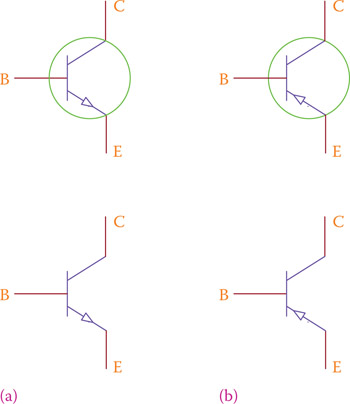
Figure 17.2
Symbols for (a) NPN transistor and (b) PNP transistor.
The emitter is identified by an arrow, which shows the direction of current. Note the difference between the two symbols. The direction of the arrow in the two transistor types are from positive to negative, or better say from P to N, where P and N refer to the semiconductor material type.
Note that for the sake of simplicity in the rest of this chapter we drop the suffix “junction” and only use the word “transistor.”
17.3 Transistor Size and Packaging
Transistors come in various packages (their physical form), the most common of which are shown in Figure 17.3. Their size is comparable with paper clips, as shown in Figure 17.4. Like any other device, a transistor has ratings for current, voltage, and power. These are defined in the data sheet of each transistor and must be respected when used in electrical and electronic circuits. Transistors may get hot when operating. In such a case a heat sink may be attached (screwed or glued) to its body. A heat sink is not part of a transistor; it is used for any component that can get hot in operation. It is a piece of metal (normally aluminum) with a large area (so that it can easily exchange heat with its surrounding environment), sometimes corrugated, which is attached to the body of a component that can get hot. This is a common practice, particularly in electronic devices. A heat sink can be air cooled or in very high power devices can even be water cooled. Figure 17.5 shows a resistor with a large heat sink. Part of the reason for different packaging of transistors is the heat that they produce in operation. Only three of the transistors in Figure 17.3 can accept a heat sink.
Heat sink: Piece of aluminum attached to an electronic component to provide a larger area of contact with air, so that the heat produced in the component is removed from it better and faster and overheating and damage is prevented.
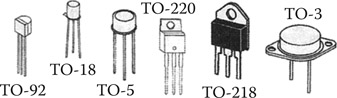
Figure 17.3
Examples of physical shape (packaging) of transistors.
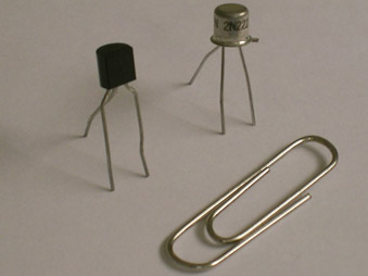
Figure 17.4
Indication of the size of a typical transistor.
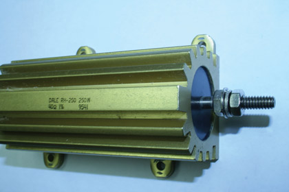
Figure 17.5
Example of a heat sink for a resistor.
For transistors with three in-line terminals (all three in a row; see Figure 17.3), usually, the connection in the middle is the base, and the other two could be marked or unmarked. But, this is not always the case. One must determine the base, emitter, and collector terminals before use.
17.4 Transistors Connection and Biasing Configuration
Because a transistor has three terminals, three different voltages can appear at each terminal when inside a circuit. In other words, on the basis of the currents in the circuit the voltage at each terminal can be different than the other two. The normal operating condition of a transistor requires that the junction between the collector and the base be reverse biased and the junction between the emitter and the base be forward biased. In this sense, the correct connections for a PNP and an NPN transistor are different. Two possible cases are shown in Figure 17.6a and b, for NPN and PNP transistors, respectively.
In the NPN transistor (see Figure 17.6a) the base is a P-type material and the collector is an N-type material. When the voltage at the collector terminal is larger than that at the base terminal, the collector-base junction is reverse biased. Also, in this transistor the voltage at the B terminal is larger than the voltage at the E terminal. Thus, the base-emitter junction is forward biased. Note that a 0 voltage means that the emitter is connected to the reference voltage, which can be the negative terminal of the DC power supply, or the ground voltage.
Similarly, in Figure 17.6b the voltages at the B, E, and C terminals are +15, +20, and +2 V, respectively. This implies that the voltage at B (N side of the base-collector junction) is greater than the voltage at C terminal (thus, reverse bias) and the voltage at B is smaller than the voltage at E terminal (thus, forward bias).
For a transistor to function the condition is that (1) the emitter-base junction be forward biased and (2) the collector-base junction be reverse biased.
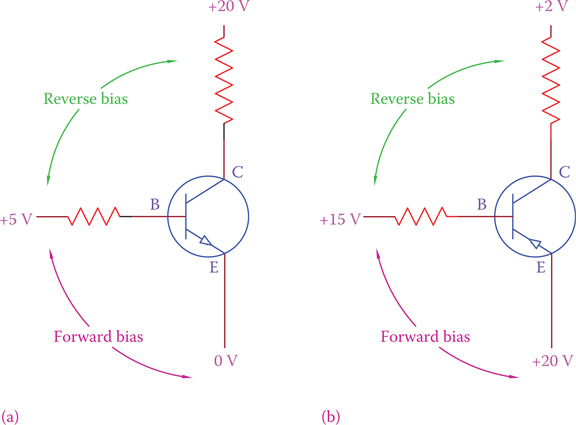
Figure 17.6
Correct connection of (a) NPN and (b) PNP transistors.
17.5 Modes of Operation
As we will learn gradually, most applications of a transistor are for switching and for amplification. In switching, a transistor is used as a switch, meaning that it can turn on and off a device or part of a circuit. As for amplification, a transistor can be used as a voltage amplifier, a current amplifier, or a power amplifier. In both switching and amplification, there is an input signal to the transistor and an output signal from the transistor. For each signal (input and output), two connections are necessary, as shown in Figure 17.7. This figure symbolizes a transistor as an input-output device, each one with an internal resistor between the two terminals. When a signal is introduced to the input terminals, the corresponding output signal is generated and is available at the output terminals. Because a transistor has only three physical terminals to the outside world, in order to have two input lines and two output lines, two of the terminals can be assumed to be internally connected, through an internal resistor. In other words, one of the terminals must be shared between the input and the output.
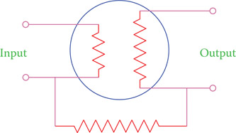
Figure 17.7
Input and output concept in a transistor.

Figure 17.8
Three modes of operation of transistors: (a) common base, (b) common emitter, and (c) common collector.
In a circuit containing a transistor, in order that the correct biasing as mentioned above is respected, the transistor can be used in three different ways. These different ways are based on which terminal is shared between the input and output and define three modes of operation of transistors. These three modes are common base, common emitter, and common collector. As the name implies, in each mode one of the terminals is common for both input and output.
Common base: One of the three configurations for using transistors in a circuit, where the base is a part of both the input and the output.
Common emitter: One of the three configurations for using transistors in a circuit, where the emitter is a part of both the transistor input and its output.
Common collector: One of the three configurations for using transistors in a circuit, where the collector is a part of both the transistor input and the output.
Figure 17.8 shows the three modes of operation for an NPN transistor. The same three modes are possible if a PNP transistor is used, but they are not shown here. In Figure 17.8a the input signal is introduced between the emitter and the base and the output is taken between the base and the collector. The + and − signs shown are for the voltage, which must be such that the corresponding junctions, have the correct bias. It is obvious that the voltages and currents must be compatible so that the base can be connected to both the input circuit and the output circuit. The same principle applies for the common-emitter and common-collector configurations. Later, we see that both correct biasing and voltage compatibility are achieved by having the appropriate resistors or other components in the circuits of each of the three terminals.
17.6 How a Transistor Works
The function of a transistor is like a gated device to the electric current. If the gate is open, there is a flow, and if the gate is closed, there is no flow. The role of the transistor input signal is to open and close the gate, as desired. The output is, thus, controlled by the input. When the gate is open, energy is delivered to the output (e.g., to a load). From the power viewpoint the important fact in the operation of a transistor is that the input power is much smaller than the output power.
Figure 17.9 shows a transistor circuit. The collector is connected to the positive side of a 12 V battery through a resistor R2, and the emitter to the negative side. At the same time a smaller (1.5 V) battery is connected between the base and the emitter through the resistor R1 and a switch. The polarity of this battery is such that the base-emitter junction is forward biased, that is, positive side to the base. In this sense, there are two loops formed for the electric flow, one between the collector and the emitter, and one between the emitter and the base (emitter is the common terminal).
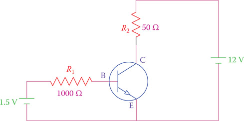
Figure 17.9
Connecting a transistor to electric supply.
While the collector-emitter loop is closed (and there is no switch), no current flows from the collector (positive side) to the emitter. Also, in the base-emitter circuit, there is no current when the switch is open. Now, if the switch is closed, a small current of 0.8 mA (that is, [1.5 V − 0.7 V]/1000 Ω, assuming a silicon-based transistor) can flow through R1from base to the emitter. This current from the base to emitter can cause conduction in the transistor between the collector and the emitter (the second loop). Its function is, in fact, similar to opening a gate, as a result of which a current of around 240 mA (i.e., 12 V/50 Ω) flows from the collector to the emitter. In other words, closing the switch in the first loop causes a current in the second loop.
Consider now the power in the two loops, by multiplying the loop current and its voltage. It is evident that the power in the second loop (12 V × 0.240 A = 2.88 W) is much greater than that of the first loop (1.5 V × 0.0008 A = 0.00120 W).
The above explanation shows the way a transistor works. That is to say, the functioning of a transistor is based on currents in the two loops and not the voltages. This implies that a transistor is a current driven device. Note that in this simple analysis we have ignored the internal resistances in the junctions between the three elements (base, collector, and emitter) of a transistor. In reality, there is always some resistance between these elements. It is also imperative to note that the transistor, itself, does not generate power. All the power necessary for amplification comes from the battery (the power supply).
When there is no current between the base and the emitter in a transistor, the transistor is off. When a current flows between the base and the emitter, a current also flows between the collector and the emitter.
A transistor is a current-driven device.
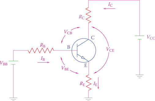
Figure 17.10
Definition of voltages and currents in a transistor.
17.7 Transistor Properties
Figure 17.10 depicts the definitions for various voltages and currents in a transistor. The voltage between the base and the emitter is denoted by VBE. The voltage between the collector and the emitter is denoted by VCE, and similarly the voltage between the collector and the base is denoted by VCB. Likewise, the currents flowing through the base, the collector and the emitter are, respectively, represented by IB, IC, and IE. Moreover, as indicated in Figure 17.10, the total voltage supplying power to the collector is called VCC and that corresponding to the base is called VBB. By the same token in other transistor configurations a supply voltage may be used for the emitter. In such a case this voltage is represented by VEE.
On the basis of the discussion in Section 17.6 and the voltage drop in a PN junction (0.7 for silicon and 0.3 V for germanium), if VBE, is less than 0.7 V (assuming a silicon transistor), no matter how much the voltage between the collector and the emitter is (provided that it is within the rating of the transistor and does not cause a breakdown), no current flows from collector to the emitter. In such a case the transistor is said to be in the cutoff state.
Cutoff: Status of a transistor when it is not operating because of very low (negligible) current.
As soon as VBE becomes larger than 0.7 V, a current (IB) flows from B to E. This is the current through the base. This current turns the transistor on and causes conduction between the collector and the emitter. Thus, the current IC flows through the collector toward the emitter. The current in the emitter, IE, is the sum of IBand IC.
The current in the emitter is the sum of the current in the base and the current in the collector.
It is important to understand the operational characteristics of a transistor. In addition to the fact that it behaves as a gated device, we must also know that a transistor behaves like a variable resistor. This is concerning the voltage VCE and the current from the collector to the emitter (IC). When a transistor is conducting, the current flow from the collector to the emitter is the major component of interest. This is the output current. There is a voltage drop between the collector and the emitter when this current exists. Nevertheless, this voltage drop cannot be determined based on the assumption that there is a constant resistance between the collector and emitter terminals inside the transistor. The value of such a resistance is not constant. This matter will become clearer later.
A transistor behaves like a variable resistor as far as the relationship between the collector-emitter voltage and collector current is concerned.
As has been shown in Section 17.5 and Figure 17.9, a noticeable characteristic of a transistor is that IC is much larger than IB (it can be 100 times or 200 times larger). Moreover, the ratio IC/IB, which is almost constant for a transistor in a given circuit, is denoted by the Greek letter β (beta) and can be used for calculation of ICwhen IB is known, or vice versa. β depends on the particulars of a circuit, transistor properties, and temperature (by particulars of a circuit we mean the components, their values and the circuit arrangement). The minimum and maximum values for parameters of a transistor are normally given in its data sheet.
| IC=βIB | (17.1) |
Moreover, because β is normally large (typically, 50 < β < 300), then
| IE=IB+IC=βIB+IB=(β+1)IB≈βIB=IC | (17.2) |
Equation 17.2 implies that, for simplification, in many calculations IE is set equal to IC. Note that the electrical values must match with reality; in practice, there are always maximum values for current and power that a device can handle, based on its internal structure and rating. In other words, one cannot rely only on mathematical relationships for a device that is bound by its physical properties, thus exhibiting limit values for current, voltage, and power that it can handle.
Example 17.1
Consider the transistor in the circuit of Figure 17.9. If the value of β for this transistor is 100 and RC= 50 Ω, what is the voltage VCE?
Solution
The base current is
IB = (1.5 − 0.7) ÷ 1000 = 0.0008 A
The collector current is β times (100×) the base current
IC = 100 × 0.0008 = 0.08 A = 80 mA
and the voltage drop in RC is
VRc= 50 × 0.080 = 4 V
VCE is the difference between the power supply voltage and the voltage drop in RC:
VCE = 12 − 4 = 8 V
Example 17.2
For the transistor in Example 17.1, what is the internal resistance between the collector and the emitter for the given condition?
Solution
On the basis of the voltage VCE = 8 V and the current IC = 0.08 A, the internal resistance between the collector and the emitter is
8 ÷ 0.08 = 100 Ω
Note that this resistance value is not constant, and changes for other operating conditions.
Example 17.3
If in the circuit of Example 17.1, the resistance RCis substituted by a 200 Ω resistor, what will be the voltage VCE?
Solution
For this case it can be seen that the voltage drop in RCis 16 V (200 × 0.08). This is greater than the total VCC voltage (12 V), which is impossible. This reflects a bad design, in which the transistor cannot function correctly, or as expected. The voltage drop in RC cannot exceed 12 V.
17.8 Transistor Main Functions
Two principal functions of a transistor are switching and amplification. Both of these have been demonstrated in the discussion of Section 17.5. The rest of this chapter is devoted to an explanation of how a transistor can be employed for these functions. First, in order to better understand what is meant by switching and amplification, we examine the following two examples.
17.8.1 Switching Function
Suppose that the current in a motor when working is 30 A. Dissimilar to a household device that you turn on and off by a simple switch, for such a relatively large load a relay is used to turn the motor on and off. A relay consists of an electromagnet that can work with a low voltage (for better safety), for instance, 12 V. The electromagnet takes little current and can easily be activated even from a distance away without a concern about voltage drop in the wire. When activated, two (or more) sets of reeds make contacts. These reeds are connected to the motor and the electric supply (higher voltage). In this way, electricity is applied to the motor through an indirect switch. A person’s hand doesn’t have to even be near to the higher voltage line. A relay is shown in Figure 17.11 together with a dime (10 cent American or Canadian coin), for size comparison.
Figure 17.12 illustrates a schematic for a relay with only two connections. This relay can be used in two ways: when activated a connection is made, or an existing connection is broken open. In the relay schematic “NO” stands for normally open and “NC” denotes normally closed. For making a connection, for instance in the case of a motor, the lines are connected between NO and the common connector (COM). Similarly, if we need to stop a connection when the switch is activated, it is connected between the NC and the COM terminals. Figure 17.13 illustrates the use of a relay for switching a motor on and off.
The advantages of using a relay are twofold:
- A person is not directly in contact with a switch carrying a relatively high voltage and/or a high current, which is accompanied by a spark when contact is made or broken.
- The switch can be installed in a remote position without the necessity for thicker wires of the motor circuit to be long. Thus, more expensive wiring and larger voltage drop in the circuit (and consequently waste of energy) are avoided.
Whereas a relay is a mechanical device, a transistor can perform the same job electronically and without any moving parts. It is smaller, too.

Figure 17.11
Picture of a small relay with eight sets of connections.
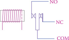
Figure 17.12
Schematic of the operation of a relay.

Figure 17.13
A relay used for activating a motor.
17.8.2 Amplification Function
Figure 17.14 shows a scenario in which by opening and closing a small valve and allowing a small flow of water a larger amount of water flow is controlled. This example shows another important function of a transistor, which is amplification of a signal. Amplification is a major part of the function of almost all electronic devices, such as radio, TV, phone, voice and data recorders.
As illustrated in Figure 17.14, the round gate G can move up and down, thus adjust the flow from the channel C that connects to a water source. The gate movement is provided by a rotational motion of the gate assembly about axis xx′. Because of the counterweight on the other side of the axis the gate can move up by a slight downward force on the right. The weight of the gate keeps it normally in the closed position and the counter-weight W is such that little effort is required to move the gate about its axis. The bottom hole in the container B, attached to the lever bar between the gate and its counterweight, lets any water remaining in it be emptied and directed downstream through the funnel D. In this sense, the gate will close unless extra downward force exists on the right-hand side. By opening the valve S a small flow of water runs into B. This causes water to accumulate in B and make the counterweight side heavier, thus, pulling the gate upward and opening it. Consequently, a large flow of water is established from upstream to the E part of the channel. When the valve S is closed again, the water in B drains out and the gate goes back to its closed position.
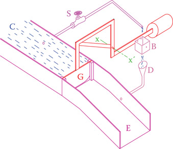
Figure 17.14
A hydraulic analogy of amplification function of a transistor.
By controlling the flow of water through the valve S we may control a larger flow of water through channel C. In other words, the variation of the output in channel C is proportional and similar to the smaller flow controlled by the valve S.
In an amplifier a low power signal is duplicated with much higher power. In other words, the input signal drives an amplifier to generate a more powerful signal with the same pattern at its output. More power implies higher voltage, higher current, or higher both voltage and current. The power that is included in the output must be provided by the power supply powering a circuit.
In an amplifier the power added to a signal is provided by the power supply.
17.9 Transistor as a Switch
In the following circuit the transistor acts as a switch, in the same way that a relay works. The advantage of a transistor to a relay is that a transistor is lighter, has less noise (if any at all), has no moving components, it is faster, consumes less energy and it is cheaper. Note that in a complicated system, such as the operation of an elevator or a train, there can be hundreds or sometimes more than a thousand relays. In the past, these relay systems were common. In addition to taking a much larger space and making noise by each relay when making contacts, after a while bugs could also make nests in the warm space between them and gradually disrupt the operation (the term bug and debug in computer terminology stems from here).
In the circuit shown in Figure 17.15 an NPN transistor is shown. The collector-base junction is reverse biased, as required, and a current never flows between the collector and the base. The base-emitter junction is forward biased, but when the switch is open there is no current between the base and the emitter. Consequently, there is no current between the collector and the emitter because the transistor acts like an insulator.
If the voltage at point A (where the load is connected) is measured, it shows 25 V because there is no voltage drop in the 200 Ω resistor (due to carrying no current). The voltage difference across the load is zero and the load is not energized.
Closing the switch lets a current flow between the base and emitter. As mentioned earlier, this action turns on the internal collector-emitter connection and causes an electric current to flow from collector to the emitter. The magnitude of this current depends on the resistance R, which is 200 Ω here. Ignoring the small voltage drops in the transistor, the C-E current is 125 mA (25 ÷ 200, based on Ohm’s law). The current flow of 125 mA causes a voltage drop of 25 V in the 200 Ω resistor. In such a case, if the voltage at point A is measured it must be 0 V.
Comparing with when the switch was open, now the voltage difference across the load is 25 V, and, therefore, the load is energized (note that when the load is connected to point A, the current through the emitter is the sum of the current through the 200 Ω resistor and the load current).
The scenario shown in Figure 17.15 is a practical example of the switching action of a transistor. Although it is a very simple example, it shows the principle of the way a transistor can be used for this type of application. A similar circuit can be used for other applications such as counting people entering a library or the cars passing through a pathway by replacing the manual switch by a photocell (a resistor whose resistance changes with light and can be used as a light sensor), or by an automatic switch of a different type. The switching action of a transistor can be at very high frequency, like the radio, TV, and communication signals with megahertz frequencies.
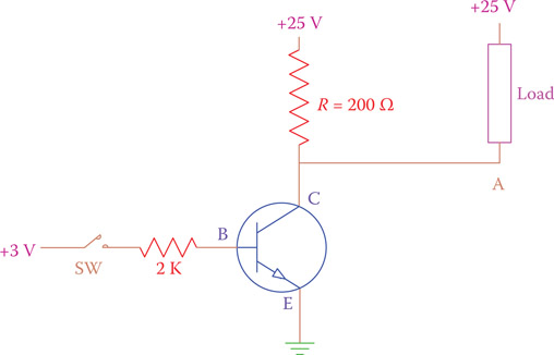
Figure 17.15
Transistor used as a switch.
In practice, we may want to avoid using more than one voltage source. This is very reasonable. Figure 17.16 illustrates the same setup as in Figure 17.15, but the voltage at the base is derived from the same power source supplying the load and the collector. In this arrangement the resistors R2 and R3 are so selected to provide the necessary voltage at the transistor base when the switch is closed. R2 and R3 resistors on the left establish a voltage divider. When the switch is closed a voltage equal to 1/8th (2000/[14,000 + 2000]) of the total voltage provided to the load is applied to the base.
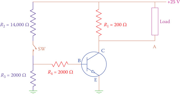
Figure 17.16
Providing base voltage by a voltage divider.
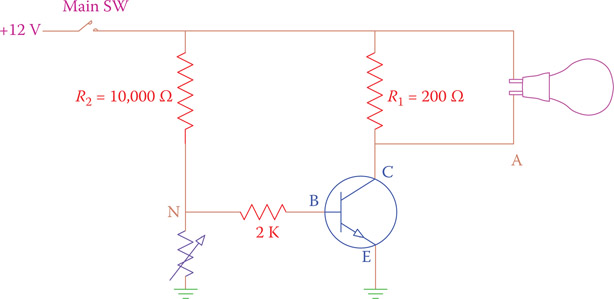
Figure 17.17
An automatic switch for turning a light on at night.
The above circuit can be used for automatic on-off switching of a light-bulb, if a photocell is inserted as a switch in the circuit. A photocell is like a variable resistor. When there is no light, it has a high resistance and in the presence of light its resistance drops. Consider the circuit shown in Figure 17.17. During the day the photocell (shown as a variable resistor) acts as a conductor, and, thus, the voltage at point N is zero (N is shorted to the ground). During the night, however, the resistance is considerable and the voltage at point N is equal to the voltage drop across the photocell resistance. As a result, current flows between the transistor base and emitter; this causes the transistor to turn on, as described.
For other applications, alternatively, the voltage at the base terminal can be provided by a sensor that generates a signal with sufficient voltage. (Remember that the junction between B and E requires 0.7 V, if made out of silicon, to conduct. The voltage at B, thus, must be more than that for a current to flow.)
17.10 Transistor Amplifier
A transistor can amplify the current or voltage of a signal. Amplifying current implies that the transistor output current is higher than its input current. Amplifying voltage implies that the voltage variation of the output is higher than the voltage variation of the input. When put together, a number of transistors can serve as a power amplifier (amplifying both voltage and current). For instance, a very weak electromagnetic signal received by the antenna of a radio has little voltage and cannot cause any significant current in a circuit. It must be amplified by hundreds of times in order to be audible through a loudspeaker. Similarly, a weak signal picked up by a sensor in many industrial applications, is amplified before it can be used for further processing. The circuit in Figure 17.18 illustrates a simple example of how the voltage of a simple sinusoidal signal can be amplified. In other words, if a sinusoidal signal is introduced as the input of a transistor, the transistor output is a similar signal (having the same form and frequency) with a higher voltage. We study the variation of the voltage across the load and compare it with the input voltage.
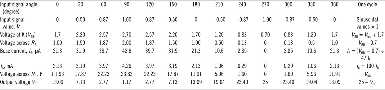
The input is a sinusoidal voltage with a peak-to-peak value of 2 V introduced at point K, which is connected to the transistor base through a 47 kΩ resistor. The other wire for this signal is connected to the ground. The role of the capacitor before point K is very important. It filters (prevents from passing) any DC content that may be blended with the input signal (see Section 13.6). The corresponding values for the input (the sinusoidal waveform) and the output (voltage across the load) for each 30° of the one cycle are entered in Table 17.1, together with some other values, as discussed.
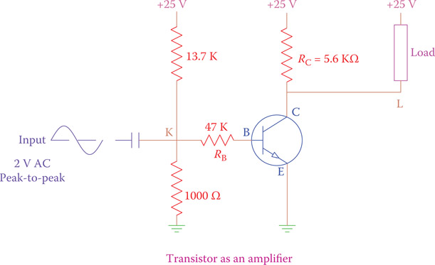
Figure 17.18
Example of voltage amplification by a transistor.
Assuming that this transistor is made out of silicon, because in a silicon base transistor there is always a voltage drop of about 0.7 V between the base and the emitter, the voltage at K must be such that it never goes below
Table 17.1 Variation of Input versus Output Voltage for the Circuit of Figure 17.18
0.7 V. Otherwise, the transistor goes to cutoff state and stops conducting. In this example the 13.7 kΩ and 1000 Ω resistors form a voltage divider to provide 1.7 V DC at point K. This value of 1.7 V has been specifically selected such that for the most negative value of the sinusoidal wave the base-emitter junction is still forward biased and its VBE is not less than 0.7 V (1.7 − 1/2 × 2) = 0.7 V; the input is 2 V peak to peak.
The 2 V peak-to-peak value AC signal and the 1.7 V DC signal add together and, as a result, the voltage at point K has a variation between 2.7 and 0.7 V.
Table 17.1 shows the following values for 12 different points (360° at 30° intervals):
- Input signal angle at various instants during one cycle.
- Input signal voltage.
- Voltage at point K.
- VBE (Voltage at K − 0.7 V).
- Base current, in micro ampere (μA), based on Ohm’s law VBE/470 kΩ.
- Collector current in mA, assuming 100× the base current (IC = βIB = 100IB).
- Voltage drop in resistor RC (see Figure 17.18).
- Voltage at point L. This is VCE, because the emitter is grounded, VCE = 25 V – voltage drop in the 5.6 kΩ resistor.
Notice that here we have intentionally connected the load across the 5.6 kΩ resistor. The variation of the voltage across the load is sinusoidal, that is, similar to the input. Although this way of connecting the load is possible, it is not the only way to do so. The load could be connected between the ground and point L, which indeed represents the output for this amplifier, based on Figure 17.8. This matter is further discussed in Chapter 18 (see Section 18.3). For this configuration both the output voltage and the voltage across the load have sinusoidal forms, but the two voltages have 180° phase difference.
Figure 17.19 shows the relationship between the voltages of the input and output signals (rows 2 and 8 of Table 17.1). There are a number of important points that can be observed from Figures 17.18 and 17.19:
- The transistor is used in a common-emitter configuration.
- The input signal has a sinusoidal waveform.
- The input signal was blended with a positive DC value to create a varying DC (varying in value, but otherwise always positive) signal.
- The output is also always positive, but it has a variation in the form of a sinusoidal wave.
- The output variation (sinusoidal pattern) has the same frequency as the input.
- The peak to peak of the output voltage variation has a larger value than that of the input signal.
- When the input signal is at its maximum, the output signal is at its minimum, and vice versa. That is, the output is 180° out of phase with the input.
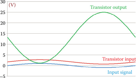
Figure 17.19
Input and output relationship in a transistor when used in common emitter design.
In the same way that the input signal was blended with a constant DC voltage, the output signal has a DC content, as seen in Figure 17.19. To remove the DC content of the output signal, a capacitor is added to the circuit at a point where the output signal is taken (point L). The revised circuit is as shown in Figure 17.20. This capacitor of appropriate value can filter out the DC content (block the DC current). The outcome of this filtration is a signal that varies between −11.9 and +11.9 V, (25−1.22), that is, its peak-to-peak value is about 23.8 V. Figure 17.21 depicts the voltages at points H, K, L, and M of the circuit in Figure 17.20; the amplification, however, is shown smaller in order fit the page. The input signal is introduced between point H and the ground, and the output signal is taken between point M and the ground. The sinusoidal input signal was amplified by 11.9 times (the ratio between peak value of the output and the peak value of the input).
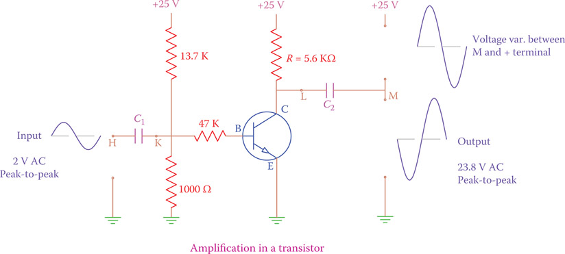
Figure 17.20
Capacitor C2 is added to the circuit in Figure 17.19.

Figure 17.21
Voltage forms at various points of the circuit in Figure 17.20.
17.11 Biasing a Transistor
The action of blending the input signal with a constant DC value (observation 3 in the previous section) is extremely important and needs more elaboration. One must understand the motivation for it. Notice that as a result of this DC value, which was added to the input signal, VBE (the base-emitter voltage) always has a positive value greater than 0.7 V (we assumed a silicon transistor). To better understand the subject, first, we consider a similar scenario, but instead of blending the input with 1.7 V DC, we add only 0.7 V, using a smaller resistor instead of 1000 Ω in Figure 17.18. The resultant of the voltage values at different points (similar to those in Table 17.1) associated with various instants of one cycle of the sinusoidal input signal are shown in Table 17.2 for this case, and the corresponding graph is depicted in Figure 17.22.
As can be observed, two main differences exist between the results of this case and the previous case: (1) only half of the signal is amplified and the other half is clipped (cut), and (2) the variation of the output signal is only between 25 and 13 V. That is, the power added to the input signal is only half of the previous case. The behavior of the transistor in this case is not necessarily unwanted. There are cases when such a performance is desired. This will be further studied in the classification of amplifiers in Chapter 18.
The action of adjusting the VBB in a transistor circuit so that the amplification be as desired is called biasing a transistor. The discussions about transistor amplification in Sections 17.10 and 17.11 are mainly to learn how a transistor works. In practice, there are many more issues to be concerned about, and it is more customary to include an emitter resistor that can also adjust the base current IB. This is shown in Figure 17.23. Note that current through RE corresponds to both IB and IC. The emitter current is obtained by dividing the emitter voltage by the value of the resistance RE, and only a fraction of this current (1/β) passes through the base-emitter junction (see Equation 17.1). The typical value for RE is 1/10th of the value of RC. Observe other differences between this and the previous figures. The voltage provided at point K is partly dropped across the BE junction and partly dropped in RE. We will discuss more about amplifier circuits in the next chapter.
Biasing a transistor: Connecting the three terminals of a transistor to the appropriate voltage to adjust/select the operating region of a transistor.
Table 17.2 Variation of Input versus Output Voltage for the Transistor in Figure 17.20, with 0.7 V DC at Point K
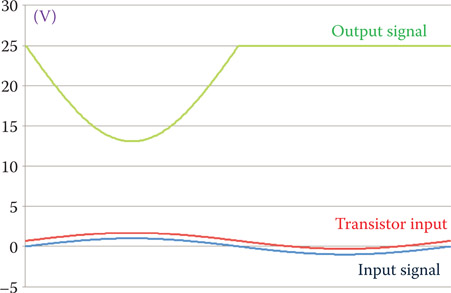
Figure 17.22
Clipping the output signal by a transistor due to different biasing.

Figure 17.23
More common circuit of a transistor amplifier.
17.12 Chapter Summary
- A junction transistor is made of two PN junctions.
- Depending on how the two PN junctions are joined together, the PNP and NPN transistors are made.
- Transistors come with different packaging, and they are small.
- A transistor has three elements: base, collector, and emitter.
- A transistor has three terminals connected to its three elements, and it is an input-output device.
- As an input-output device, one of the terminals must be shared between the input and output.
- The three operating configurations, common base, common collector, and common emitter stem from which terminal is shared between the input and output.
- The primary functions of a transistor are switching and amplification.
- For a transistor to function the collector-base junction must be reverse biased, and the emitter-base junction must be forward biased.
- Without a minimum voltage between the base and the emitter, a transistor is cutoff. It does not conduct. This minimum voltage depends on if a transistor is germanium based or silicon based.
- When there is a current between the base and the emitter, a transistor conducts, meaning that the collector and emitter are internally connected and can make a closed loop with the external circuit.
- Current in the emitter is the sum of the base current and the collector current.
- In a transistor the current in the collector is much higher than the current in the base. The ratio between these two currents is almost constant for a transistor circuit. This value is denoted by the Greek letter β (beta) and depends on transistor characteristics and the circuit it is used in, as well as operating temperature.
- A transistor behaves like a variable resister between its collector and emitter. This affects the relationship between the collector-emitter voltage and the collector current (between collector and emitter).
- A heat sink is a flat or corrugated piece of metal used for components that become hot during operation, like a transistor. It can be attached to the body of a component to dissipate the heat faster and cool the item.
Review Questions
- What are the two primary classifications of transistors?
- What are the three elements in a transistor?
- What are the principal functions of a transistor?
- How many terminals does a transistor have?
- Name the three configurations under which a transistor can function.
- Describe the correct bias condition for a transistor to function.
- What is the difference between a PNP and an NPN transistor?
- What is the difference between the symbols for a PNP and an NPN transistor?
- Is the current in the collector of a transistor greater or the current in the emitter?
- Is the current in the base of a transistor greater or the current in the emitter?
- When a signal is amplified by a transistor what property of the signal becomes larger?
- If a signal is amplified by a transistor, where does the power added to signal come from?
- What is meant by cutoff?
- If two lines are needed for input and two lines for output, how does a transistor work as an input-output device with only three terminals?
- Can you guess from what the name “transistor” is made of?
- Is the transistor in Figure P17.1 a PNP transistor or an NPN transistor?

Figure P17.1
Circuit of Problem 1.
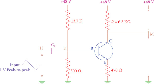
Figure P17.2
Circuit of Problems 3 and 4.
Problems
- Find the internal resistance between the collector and the emitter for the transistor in Figure P17.1 if IC = 3 mA.
- If β = 120 for the transistor in Problem 1, find the current IB.
- Without the input considered, how much is the voltage VBB (voltage at K) in the transistor shown in Figure P17.2?
- For the transistor in the circuit shown in Figure P17.2 make a table similar to Table 17.1.