
24
Encoders and Decoders
OBJECTIVES: After studying this chapter, you will be able to
- Explain what a flip-flop is and what it is used for
- Define various types of flip-flops
- Understand toggle action in a flip-flop
- Describe how a flip-flop can be used for counting
- Describe how a flip-flop can be used for storing a bit of data
- Explain how a digital clock works
- Explain the difference between a latch and a flip-flop
- Describe the function and use of an encoder
- Describe the function and use of a decoder
- Understand the precision in a shaft encoder
- Explain what a multiplexer is and why we need it
- Describe the difference between a multiplexer and a demultiplexer
New terms: Absolute encoder, active high, active level, active low, anemometer, asynchronous counter, bistable, combinational logic, D flip-flop, feedback, frequency divider, incremental encoder, J-K flip-flop, latch, reset, sequential logic, set, synchronous counter, wind vane
24.1 Introduction
In Chapter 23 we discussed logic gates, logic circuits, their mathematical functions, and how they can be used to formulate digital systems. Digital systems are the backbone of digital computers and digital industrial control.
In this chapter we discuss how data are handled and stored; for example, how an 8-bit system holds 8-bits and how codes from one form are converted to the other form. An example of the latter is how digital displays work. Considering a seven-segment display, the information in a binary form must light up different segments of the display. This requires a conversion of code from one form to another (binary to BCD).
All gates that we studied and their circuits lead to an output as a result of a combination of the actions of the elements in a circuit. For this reason, those circuits are referred to as combinational logic. In the new material an element of time plays a role, as well. Any stored data have to be maintained until they are altered. Stored data are in the form of 0 and 1. How these data can be controlled, in terms of whether and when to switch to a new value, is the subject of sequential logic, which we study in this chapter.
Combinational logic: Logic circuits made of a combination of logic gates but without any memory element, as opposed to a sequential circuit.
Sequential logic: Kind of logic circuit with timing sequence, memory, and synchronization.
We start with the study of flip-flop, which is the basic memory element.
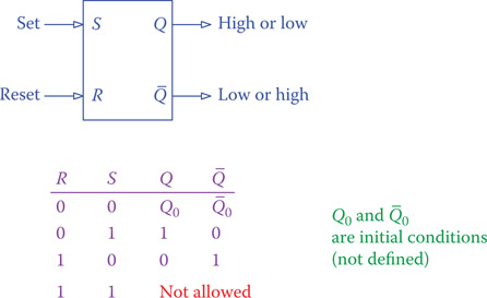
Figure 24.1
Basic flip-flop.
24.2 Flip-Flop
A flip-flop is the basic memory element for storing a bit of information. It is an edge-triggered device. That is, it reacts to the edge of a pulse. A simple flip-flop has two stable states (remember, for instance, that a capacitor has two states: charged and discharged). States are represented by 1 and 0. Stable state implies that the device remains in one state (e.g., 0) until an input changes its condition to the alternative state. Because a flipflop has two states only, it is called a bistable device.
Bistable: Having two stable (controllable) states.
A basic flip-flop has two inputs and two outputs, as shown in Figure 24.1. The two inputs are used to set or reset the device and are denoted by R and S. The outputs are denoted by Q and Q; they reflect the state of the flip-flop either 1 or 0. If Q = 1, then Q = 0, and if Q = 0, then and Q = 1. Figure 24.1 illustrates also the truth table for the states of a flip-flop.
Set: (for a flip-flop) Putting a device to a desired state. Some devices have only two states on and off, or high and low. Set implies putting the device in a desired (usually nondefault) state.
Reset: Action of putting or setting a device to its default state.
A flip-flop acts like a single-pole double throw (SPDT) switch. When activated, its output toggles. This property can be used for many operations performed in digital electronics, as we will see in this chapter. The toggle action is performed through the inputs to a flip-flop. There are a few types of flip-flops, as will be described shortly, in terms of their operational properties. The one shown in Figure 24.1 is the basic flip-flop or the simplest type.
Before continuing further we need to categorize flip-flops based on their structure, which defines the active level for a flip-flop. Active level is the logic level (high or low) that activates a device. For flip-flops it implies if a flip-flop is set, or its state toggles, with a logical high or a logical low applied to its set input. In this sense, there are two categories of flip-flops, those whose active level is 1 and those whose active level is 0, i.e., those that are active high and those that are active low.
Active level: The (high or low) level in which a logic device functions.
Active low: Implying that the active level for a device is low, as opposed to active high.
Active high: Two-state logic device (e.g., true and false, on and off, high and low) that acts (executes its function) when it is in a high state, as opposed to being active when in the low state.
24.2.1 Basic Flip-Flop
The basic flip-flop is set by applying an active level signal to its set input and the inverse signal to its reset input. When the unit is set, the Q output is high and the Q output is low. If, instead, the active level signal is applied to the reset terminal and its complement is applied to the set terminal, then the Q output is high and the Q output is low.

Figure 24.2
Internal structure of flip-flops.
Also, as shown in Figure 24.1, one cannot apply a logical high to both set and reset of a basic flip-flop at the same time. It is like simultaneously pressing the start and stop button of an electric motor.
Structurally, a flip-flop can be made of two NOR gates or two NAND gates. This is shown in Figure 24.2. The gates are interconnected to each other or, in other words, they have feedback. The output of each gate is one of the two inputs to the other gate.
Feedback: Taking the output of a device to compare with its input for the purpose of regulation and adjustment.
Note the output of the gate designated as S. For the NOR-NOR flip-flop this is Q; whereas for the NAND-NAND flip-flop, it is Q. Also, the active level for the former is 1, and for the latter is 0. In both types a set input sets the content of output Q to high. To change the value of the output to low, the reset must be used. In other words, when the flip-flop is set, if the value of the input set changes to its complement it does not have any effect on the output.
In a NOR-NOR flip-flop the active level is high, but for a NANDNAND flip-flop it is low.
A flip-flop is either set or it is reset. If it is set, it implies that the set button is activated. In this case it is meaningless to set it again. Also, it is meaningless to make reset active, too. Thus, to reset a flip-flop, first, the set must be deactivated, and then the reset must be activated. Deactivation takes place by removing (turning off) the input signal.
Likewise, to set a flip-flop after it has been reset, first, the reset must be deactivated (this by itself has no effect and does not change in the status of the output), and then, if set is activated, it sets the flip-flop (it is meaningless to activate set if the reset is still active).
A flip-flop is set by the set input when the reset is not activated. It is reset by reset input when set is not activated.
Note: In a pushbutton the activation is performed by pushing, but immediately a spring brings the button to deactivated position after being released. A flip-flop does not have the spring action; thus, the deactivation has to be separately performed.
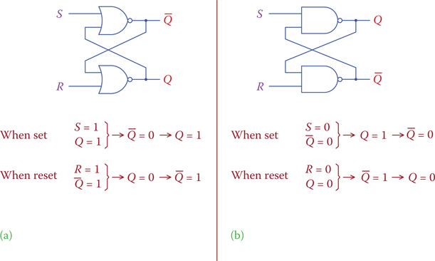
Figure 24.3
Stability reinforcement in (a) active high and (b) active low flip-flops.
What was said above can be observed in Figure 24.3 for both a NORNOR gate and for a NAND-NAND gate. Each gate has two inputs. One of the inputs, being either Q or Q, reinforces the stability of the output.
Figure 24.3 also shows that when a flip-flop is set, if S changes, nothing happens, and when it is reset, if R changes, nothing happens.
24.2.2 Clock-Controlled Flip-Flops
Clock-controlled flip-flops are more appropriate for synchronized operations, which is the case in microprocessor-controlled systems. The action of a flip-flop takes place with the clock pulse; therefore, it is in synchronism with all other operations (by other flip-flops). Setting, resetting, or toggling are the three actions of a flip-flop; depending on the inputs one is carried out at either the rising edge of the clock pulse or the falling edge of the clock pulse. This depends on whether a flip-flop is positive edge sensitive or negative edge sensitive. The symbols for the two are depicted in Figure 24.4.

Figure 24.4
Symbols for positive and negative edge triggering flip-flops.
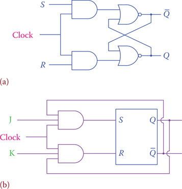
Figure 24.5
(a) Adding a clock input to a flip-flop and (b) structure of a J-K flip-flop.
For a desired action the data for the flip-flop inputs (0 and 1 values) are applied to them before the clock pulse enables the action. The clock input, shown as clk in Figure 24.4, is sometimes referred to as enable because it enables an action to take place. With the clock pulse, if the set input is activated, the flip-flop sets, and if the reset input is activated, it resets.
Figure 24.5a indicates how a clock or an enable signal is added to a flip-flop. This is shown only for a NOR-NOR flip-flop, but a NANDNAND flip flop has a similar structure. Figure 24.5 also illustrates how a basic flip-flop can be used with two AND gates in forming a J-K flip-flop.
A J-K flip-flop is clock controlled and has the advantage that unlike the basic flip-flop it can accept both inputs (now called J and K inputs) to have an active level signal. This combination is prohibited for a basic flipflop. The effect of having both inputs activated is a toggle of the output state. In a J-K flip-flop, J input is used as set and K input as reset. When both J and K inputs are active, the flip-flop toggles its output (each output switched to its complementary value, no matter what its current value is). The symbol and the truth table of a J-K flip-flop are shown in Figure 24.6.
J-K flip-flop: Flip-flop with two data entries, one for set and one for reset the output. It is also possible to toggle the output by activating both inputs.
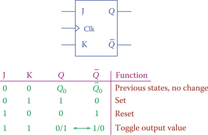
Figure 24.6
J-K flip-flop.
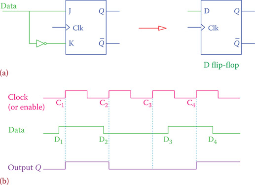
Figure 24.7
(a) Structure and symbol for D flip-flop. (b) Example of a D flip-flop timing diagram.
A data or D flip-flop is a clocked J-K flip flop that has only one input. The arrangement is as shown in Figure 24.7a, which indicates how the one output relates to the J and K terminals. The property of a D flip-flop is that the output follows the input. That is, with the clock pulse, the output will be whatever (0 or 1) has been placed on the input. Figure 24.7b shows this; even if the input (data) changes at points D1, D2, and so on, the output values update does not occur until the rising edge of the clock pulse, at C1, C2, and C4 (assuming the device is rising edge sensitive).
D flip-flop: Data flipflop: a flip-flop with only one input whose output follows the input after the enable or clock signal.
T flip-flop: A flip-flop that can toggle. It has one data input and a clock input. It toggles its output when data input is 1 after clock input allows.

Figure 24.8
Structure of a T flip-flop.
Another product based on a J-K flip-flop is a T flip-flop. Similar to D flipflop it has a clock input and only one data input. If the input is logic 1, then at the active clock pulse edge the output is toggled. Figure 24.8 depicts the structure for a T flip-flop and the truth table indicating what happens after the clock signal enable the flip-flop action based on the input and the output state. Note that a T flip-flop is based on a D flip-flop in which Q follows D.
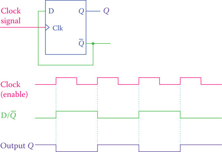
Figure 24.9
Toggle action with D flip-flop.
As we have observed, a J-K flip-flop toggles its output when both J and K inputs are set high. The toggle action takes place with the active edge of the clock pulse. Also, the T flip-flop toggles its output when the T input is high. Again, the action is carried out at the clock pulse edge. There is another arrangement where a flip-flop toggles with the clock pulse. This is with a D flip-flop as shown in Figure 24.9, in which the complementary output is fed back to the data input. Because the output must follow the input, as the clock enables the action Q takes the value of Q, thus toggling. Notice that when a flip-flop toggles the frequency of its output pulse train is 1/2 of the clock frequency.
24.2.3 Initialization
Normally, when a logic circuit becomes active, for example, at power up, the initial condition of a flip-flop is not defined or not known. We may need to make sure in what state it is before proceeding with operations. For this reason, two other inputs are added to flip-flops, a preset and a clear. If the preset is activated it forces the output to go high (Q = 1), and if the clear is activated it forces the output to low (Q = 0). Clear and preset override the clock action. Figure 24.10 shows the symbol for a D flip-flop with these two entries and a sample timing diagram indicating their effect.
24.3 Latch
Flip-flops are devices that trigger with the edge of the enable (or clock) signal. In other words, they are edge-sensitive devices. Similar devices exist that are level sensitive instead of being edge sensitive. These are called latch. Giving this name stems from the fact that they hold the status after the input is removed. This is in contrast to a switch that when its contact is broken the corresponding effect is terminated.
Latch: Term in electronics when a device retains the effect of an input after the input has stopped; like the case of a pushbutton that is pressed to make a circuit, but when it is released, the circuit is not broken because another device (like a magnetic switch) maintains the connection.

Figure 24.10
Flip-flop with preset and clear.
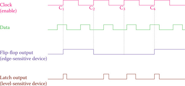
Figure 24.11
Comparison of the outputs of a latch and a flip-flop.
Figure 24.11 compares the actions of a flip-flop and that of a latch. Whereas for a flip-flop the change of the output state occurs when the clock signal edge enables it, for a latch the output is high as long as the clock has a high level and the input is high. For a flip-flop the clock pulse edge allows the output to go high if the input is already high. A rising edge sensitive flip-flop has been assumed in Figure 24.11.
24.4 Flip-Flop Applications
We can now look at a few examples of the applications of flip-flops as a storing device to hold data. A flip-flop can hold 1 bit of information. For N number of bits, thus, N numbers of flip-flops are needed.
Figure 24.12 indicates a register to hold 8 bits. As an example, the binary number 0110,1011 has been entered by some means, such as a switch set, or received from another device. The register holds the number for further processing.

Figure 24.12
An 8-bit register for binary number storing.

Figure 24.13
Flip-flops used as a random event counter.
As a second example, consider the cascade of four D flip-flops in which the complementary output from each is the data or the clock input to the next. This arrangement can be used for counting. Two types of counting may be addressed, random event counting and clock counting. Figure 24.13 illustrates how a random event counter works. This can be used for counting people entering a building, for instance.
In the arrangement in Figure 24.13 all flip-flops toggle when their clock input receives an active signal. The flip-flops are numbered for ease of referencing. The complementary output of each D flip-flop is fed back to the data input as well as serving as the clock signal of the following flipflop. In this way the stored value of each flip-flop is transferred to the next when it toggles from 1 to 0.
F1 toggles with each entry from the external sensor. F2 toggles with each change of state Q1 of F1 from 1 to 0; that is, for each two times toggle of F1 it only toggles once. Likewise, F3 toggles with each change of state of Q2 from 1 to 0. Thus, it toggles once after F1 has toggled 4 times and F2 has toggled twice; and so forth. In this way the numbers stored in the output of the flip-flops is a binary number that represent the total count of events picked by the sensor. This set of four flip-flops can count up to 16. After 16 counts (1111b = 15 is reached) the number goes back to 0. The total count can be extended by adding more flip-flops in the same way. Adding one more flip-flop extends the maximum count to 32. The count capacity is, therefore 2N, where N is the number of flip-flops.
The flip-flops do not need to be D type. Any flip-flop that can toggle its states with the clock pulse can be employed for this purpose. Figure 24.14 depicts the circuit with gated set-reset flip-flops (gated implies it has clock input). Equivalently, a J-K flip-flop can be used, as shown in Figure 24.14b. In this case the two inputs for J and K must be held high, so that the flip-flop toggles with the clock pulse. Figure 24.14c indicates the contents of the flip-flop outputs and the count number starting with a clear signal that has set all the flip-flops to 0.
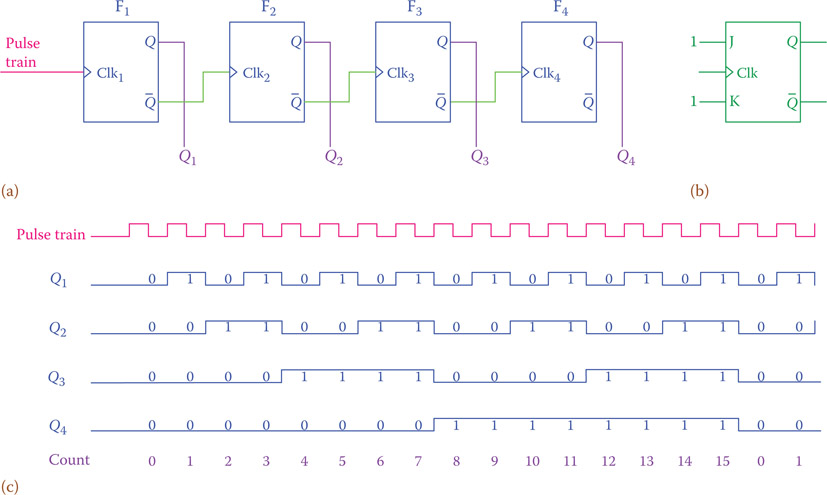
Figure 24.14
(a) Counting up circuit, (b) if J-K flip-flop is used for counter, and (c) toggle action at various flip-flops.
Any flip-flop that has a clock enable input and can toggle its output with the clock pulse may be used for counting.
In Figure 24.14 a pulse train is shown as the main input. This implies that in addition to random count this circuit can have other applications. For example, a frequency divider uses this circuit. Observe the frequency of the outputs from the succeeding flip-flops. Each one has a frequency one half that of the previous one. Note that alternative of this circuit is also possible, for example, if the output (instead of the complementary output) of each flip-flop drives the clock signal of the next device.
Frequency divider: Electronic device (normally made up of flip-flops in digital electronics) that generates waveforms of lower frequency from a higher-frequency waveform.
With this circuit it is possible to count down instead, as well. One way is to initially preset all the flip-flops to high, instead of clearing them. Another way is to use the complements of the output for counting (that is, if the readings are taken from the complementary outputs instead of Q1 to Q4). In such a case, the initial count is 15, and with each active edge of the clock it is reduced by 1 until 0 is reached. The next clock pulse then changes all the states to 1 (thus, number 15 again) and the process repeats.
Another application of the preceding circuit is the construction of a digital clock/watch. If the input to the first flip-flop is a pulse train with a constant frequency, the counting can be decoded to hours, minutes and seconds, and displayed. Decoding and conversion to display is discussed in Section 24.5. The clock pulse generator can be a circuit containing a quartz crystal, as that in digital watches, or the mains frequency (50 or 60 Hz) can be used for this purpose, as in many digital clocks. The former is more precise because it uses a quartz crystal whose frequency is in megahertz, but more divisions are necessary to bring the frequency to around 1 Hz, for the measure of 1 sec.
As can be observed from Figure 24.15, at some point it becomes necessary that the counting be interrupted and reset to 0. This is because the result of all counting is in binary; thus, the natural count goes up to 32 or 64, if we have 5 or 6 flip-flops, respectively. For example, using the 60 Hz line frequency in North America corresponds to a count of 60 for 1 sec. Thus, after counting up to 60, the seconds display is advanced by 1 and the counting process is reset to start from zero again. The same must be done after 60 sec are counted for 1 min, and after 60 min are counted for 1 hour.
For the hours, assuming 12-hour display, after the number count has reached 12, it cannot go to 13 and must start from 0 again. This sort of action is possible by adding a logic circuit so that when the count has reached its maximum allowed, a clear signal is activated to clear all flip-flops corresponding to that part of the circuit. This is shown in Figure 24.16.
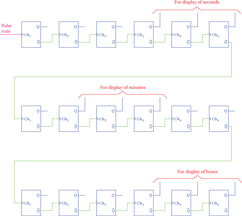
Figure 24.15
Basic circuit of a digital clock.

Figure 24.16
Interruption of counting by sending a “clear” signal to all flipflops after a desired count is reached.
In Figure 24.16 the binary number reached by four flip-flops for the display of hours is 10102. We need to stop this number from increasing to 13. The solution is that after this condition is reached an enable signal is generated and sent to the clear terminal for all the four flip-flops. The clear input was not shown in the basic configuration in Figure 24.15 for more clarity, but as you expect a clock has more circuits than shown, for example, to set the clock to a desired hour.
Note that in Figure 24.16 the inputs to the AND gate are Q1, Q3, Q2, and Q 4, corresponding to 12 = 1010b.
The arrangement shown in Figure 24.16 is also used in a frequency divider for dividing a frequency by a number that is not a power of 2. For instance, in Figure 24.14 it was shown that a waveform of pulses can be converted to another waveform with a frequency 16 times smaller. However, if we need to divide a frequency by 12, then we need to modify a circuit, similar to what was shown in Figure 24.16. A counter that counts up to N is referred to as MOD-N counter. For example, the counter in Figure 24.16 is a MOD-12 counter.
Figure 24.17 illustrates the difference between the output waveforms for a MOD-16 and a MOD-12 counter. Comparing the period (one cycle) of the square wave outputs, the first one (Figure 24.17a) corresponds to 16 counts and the second one corresponds to 12 counts.
The type of counter that we have studied is called asynchronous counter. The reason is that the toggling operations in various flip-flops do not take place at the same time; each one acts after receiving an enable signal from the previous flip-flop. In reality, there is a slight time delay in each operation, and, as a result, if the pulse train frequency is high and there are many flip-flops involved, an ambiguity in states can occur. In such a case a synchronous counter is used in which all the transactions are synchronized to happen at the same time governed by a clock pulse.
Asynchronous counter: Electronic circuitry that can store binary numbers (used, for instance, for counting random events) consisting of a number of cascaded flip-flops. The change of state in various flip-flops does not occur at the same time, as opposed to synchronous counter.
Synchronous counter: Binary counter made up of flip-flops arranged such that all flip flops change state at the same time. Synchronization is governed by the clock pulse.
In a synchronous counter depending on how many flip-flops are involved, the outputs of certain flip-flops can be AND’ed together so that

Figure 24.17
Comparison of the outputs of (a) MOD-16 and (b) MOD-12 counters.
data transfer from one to the next is delayed and then performed when the AND gate allows. Otherwise, some flip-flops toggle before they are expected to do that. An example is shown in Figure 24.18 for a counter with four J-K flip-flops.

Figure 24.18
Synchronous counter. (a) Circuit and (b) timing diagram of a synchronous counter.
In this arrangement the outputs of flip-flops F2 and F3 are not directly taken to their succeeding flip-flop. Instead, they are routed through two AND gates. As can be observed from Figure 24.18b, at the time shown as T1 the output Q2 is high, and therefore flip-flop F3 would toggle if the AND gate A1 was not there. Also, at time T2 the output Q3 is high, and flipflop F4 would toggle if the AND gate A2 was not there. But, AND’ing the appropriate outputs delays T1 until T1′ for when both Q1 and Q2 are high. The same is true for the second AND gate.
24.5 Code Conversion
As we have learned so far, data can be stored in the form of binary numbers. Depending on the number of digits available, the magnitude of information stored changes, but more information can always be stored with less data. Having 4 bits of storage (say, four flip-flops), for example, offers the possibility of 24 = 16 possible cases, not 4. The binary data are called code. Code conversion refers to the translation between the data stored in bits and the data for an application, in other words, conversion of data from one form to another.
A good example is the conversion from four bits of information that are available on four lines lighting up 10 decimal numbers (from 0 to 9) on a seven-segment LED. Although four bits (lines) can hold up to 16 numbers, all 16 do not necessarily need to be utilized. A seven-segment LED has seven LED bars, but not all must be turned on. The code converter receives the inputs for a number to be displayed and depending on the input states (corresponding to the number) determines which bars must be lit.
24.5.1 Decoder
In general, a binary code of N bits can represent 2N distinct values. A decoder is a combination circuit that converts the binary information from N inputs to a maximum of 2N distinct outputs. In a way it extracts information from a packaged data.
A decoder is a combination circuit meaning that it consists of various gates that put together a number of conditions carried by the input code. Figure 24.19 depicts the circuit for a decoder, which translates from BCD (binary-coded decimal) to decimal numbers. This circuit is good for lighting up one light out of 10 or opening a door out of 10 doors, for example, corresponding to each number. Comparing with 10 switches and 10 lines, the same function is performed with only four lines.
As another example consider a decoder that converts from binary digits to a seven-segment display to illuminate numbers 0 to 9, that is, for lighting up a one digit decimal number.
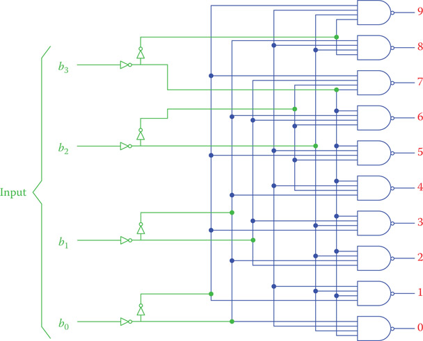
Figure 24.19
Circuit for BCD to decimal decoder.

Figure 24.20
Truth table for BCD to seven-segment display.
The decoder logic circuit is defined based on writing the requirement for each output element and simplifying the resulting logic expression. For example, the requirement for a decoder to light up a seven-segment display is as shown in Figure 24.20. For each single digit number, certain segments in the display must be lit. The segments are named a to g, as shown in the figure. Those that must be lit are tabulated for all digits from 0 to 9.
Study of the table in Figure 24.20 reveals that it shows the truth table of the decoder circuit. Each segment in the display (a to g) can be expressed as a function of the four inputs. A Karnaugh map can be used to simplify the logic expression. This is done for segment a as an example.
Example 24.1
Find the logic expression for segment a in a seven segment display.
Solution
From the truth table we see that segment a must be lit in eight cases. These are shown in the Karnaugh map in Figure 24.21a. Before filling the rest of the cells in the K-map we notice that the combinations starting with 11 do not exist. Also, the combinations 1010 and 1011 do not exist (the binary combinations for numbers 10 to 15 do not exist). All the corresponding cells, therefore, can be filled with “don’t care” X. But before that, we are going to alter the arrangement (swapping b1 and b2) in the K-map and draw it as shown in Figure 24.21b. This is a rearrange ment of input combinations to have the two 0’s on the same row, for simplification. This figure also shows the logic values (0 and 1) of the inputs on the right and bottom of the K-map. The don’t care cells are now filled with X’s in Figure 24.21c. The next step is simplification by grouping. The cells are grouped as in Figure 24.21d, which leads to the following expression:
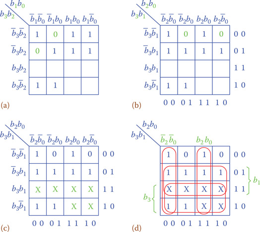
Figure 24.21
K-map for segment a of seven-segment display. (a) Information from Figure 24.20. (b) Swapping b1 and b2 for bringing both 0’s to row 1. (c) Entering X in cells with “don’t care” values. (d) Grouping cells for simplification.
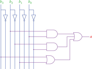
Figure 24.22
Logic circuit for segment a.
The logic circuit for segment a is illustrated in Figure 24.22.
24.5.2 Encoder
An encoder does the reverse of a decoder. It has 2N or less inputs containing information, which are converted to be held by N bits of output.
The best example of an encoder is what is used to measure the rpm of a rotating shaft or to find the angle position of a shaft in one revolution. The first one, called incremental encoder, can be used in an anemometer, a device that measures the wind speed. The second one, called absolute encoder, can be used in a wind vane to detect the wind direction. There are plenty applications of encoders in industry and home devices. Without going into much detail we briefly study the encoder part of the second type.
Incremental encoder: Type of encoder (for a rotating shaft) that adds the number of revolutions and determines the total displacement of a shaft during a given time. This is as opposed to an absolute encoder that determines the displacement (and position) of a shaft within only one revolution.
Anemometer: Device to measure the wind speed.
Absolute encoder: Determines the angular position of a shaft or rotating body in its 360° angular displacement as opposed to incremental encoder.
Wind vane: Instrument for detecting the direction of wind, consisting of an aerodynamic body that rotates about an axis and can orient itself with the wind direction.
This encoder generates a four- or five-digit binary code that can be transmitted with the same number (4 or 5) of wires carrying 0 and 1 values, which then can be decoded to find the angle position of a shaft within 360°. The resolution of measurement depends on whether four or five (or other) number of digits are used. The more the number of digits (and the wires) the more accurate the reading is. For four digits, each reading corresponds to 360 ÷ 24 = 22.5°. For five digits, each reading corresponds to 360 ÷ 25 = 11.25°.
The physical part of the encoder consists of a flat round disk on which four or five tracks are painted. Each track is divided into a number of black and white segments and a sensor can detect if a segment is black or white, which stand for 0 and 1. The arrangement of segments is such that each position of the disk (within the possible resolution) can be defined by a unique combination of 0’s and 1’s.
Figure 24.23 shows a disk with four tracks. Two types of segments are shown, one called binary code and the other gray code. With this type of encoder the gray code (which uses a different code than the binary numbers) offers an advantage that makes it more desirable in application. The advantage of the gray code over the binary code is in that moving from one number to the next implies only one bit change and not more than one. This allows detecting of any error if takes place in data reading and number processing.
For better clarity and comparison of the binary code and gray code the tracks containing black and white segments are shown straight (instead of round) in Figures 24.24 and 24.25.
Table 24.1 shows the difference between the binary code and the gray code.
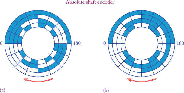
Figure 24.23
Tracks on a shaft encoder: (a) binary code and (b) gray code.

Figure 24.24
Representation of binary code tracks on the disk of a shaft encoder.
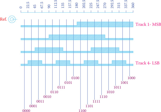
Figure 24.25
Representation of gray code tracks on the disk of a shaft encoder.
Table 24.1 Four-Digit Binary and Gray Code Comparison
| Decimal | Binary Code | Gray Code |
| 0 | 0000 | 0000 |
| 1 | 0001 | 0001 |
| 2 | 0010 | 0011 |
| 3 | 0011 | 0010 |
| 4 | 0100 | 0110 |
| 5 | 0101 | 0111 |
| 6 | 0110 | 0101 |
| 7 | 0111 | 0100 |
| 8 | 1000 | 1100 |
| 9 | 1001 | 1101 |
| 10 | 1010 | 1111 |
| 11 | 1011 | 1110 |
| 12 | 1100 | 1010 |
| 13 | 1101 | 1011 |
| 14 | 1110 | 1001 |
| 15 | 1111 | 1000 |
24.6 Multiplexer and Demultiplexer
Multiplexer and demultiplexer are two devices very important in data communications. As the name implies, their functions are opposite to each other (similar to encoder and decoder). These devices are used for sharing a device between two or more applications. Consider, for instance, a decoder for seven-segment display as discussed before. If we have a four-digit decimal number to display then we need four seven-segment displays and each one requires a decoder. However, by using a multiplexer and a demultiplexer, one unit of a decoder can be shared between the four displays.
The role of a multiplexer is to receive the information from different senders and deliver it to its output. By receiving a select data, a multiplexer is instructed from which sender to receive data. We may say, a single multiplexer (we may have multiple units of multiplexer) at a time selects information from one of many input lines and directs it to a single output. The select data then can successively address other inputs. N select lines can address 2N data input lines as senders of information.
The role of the demultiplexer is to receive information from one line input and deliver it to one of many output lines or devices as specified by the select data, which is also received by the demultiplexer. By receiving a select signal a demultiplexer channels the main data to a particular address. In other words, a simple demultiplexer receives one channel of input data and directs it to one of the many output channels, as selected by the select data. Depending on the select data bit size a maximum of 2, 4, 8, 16, 32, and so forth can share the main data.
Figure 24.26 shows the schematic of a pair of multiplexer/demultiplexer for transferring data over a single line.

Figure 24.26
Schematic of a multiplexer and a demultiplexer.
In the arrangement in Figure 24.26, if the select data in the multiplexer have a pattern based on which the data lines are continuously selected in an orderly manner, the same pattern can be given to the demultiplexer, and consequently after synchronization all data are sent and received over the line between the two. This is what happens in communication devices.
Figure 24.27 illustrates a very simplified circuit for the example of the driver for a seven-segment display. The multiplexer in this example directs a set of four incoming data to its output, which goes to the decoder (driver). After decoding is done, the information for a to g segments are put on a data bus (a bus is a main line in an electric or electronic device that provides voltage or data to all components) that is shared between the four display units. Only one of the units will light up at a time because the select data are also sent to the demultiplexer, based on which only one of the display units is connected to the positive voltage. In here it is assumed that the display segments have a common anode that needs to be connected to the positive terminal. In general, the LED’s in a seven-segment display can be connected in two ways. They have either a common anode or a common cathode. Their other sides are then connected to the driver data bus.
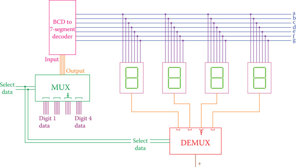
Figure 24.27
Simplified circuit showing multiplexer and demultiplexer for seven-segment display units sharing a driver.
24.7 Chapter Summary
- A flip-flop is a device to hold (store) one bit of information in the form of 1 and 0.
- When a simple flip-flop is set, its output is 1; when it is reset, its output is 0. The output is available for connection to another device.
- The output complement is also accessible for reading or using.
- A simple flip-flop is a set-reset device and does not have a provision for a clock signal.
- A clocked flip-flop has an input for clock signal or enable signal. Its function takes place at the active clock (enable) signal either at the rising edge or the falling edge of the clock signal.
- The active level is the logic level (high or low) that activates functioning of a device.
- A data flip-flop, also called D flip-flop, has only one input. Output takes the value of the input as the clock signal activates it.
- Other flip-flops are J-K and T flip-flops. A J-K flip-flop toggles when both of its inputs are logic high. A T flip-flop toggles when its only input is logic high.
- A significant property of the above flip-flops is that they toggle their outputs (swap its value). Flip-flops can be used for counting, time keeping, and frequency dividing (generating another signal with smaller frequency).
- A latch is a device similar to a flip-flop, but it is level sensitive. Its function can be performed when the clock signal has an active level.
- An encoder is a device that places up to 2N binary data on N data lines.
- A decoder extracts up to 2N binary information (made by an encoder) from N received data.
- A shaft encoder has a round disk with a number of tracks shaded differently in black and white segments. An incremental encoder is used for rpm measurement and an absolute encoder is used to determine the angular position of a shaft during one revolution.
- A multiplexer is a device to select one set out of several sets of received input data and to send it to its output. A particular input is selected based on the select data also received by the multiplexer.
- The function of a demultiplexer is opposite to that of a multiplexer. It receives one set of input data and directs it to one of the many outputs, as specified by the select data.
Review Questions
- What is the main function of a flip-flop?
- What is the principal difference between a flip-flop and a switch?
- What is meant by toggle?
- How many inputs does a J-K flip-flop have?
- What is preset in a flip-flop used for?
- What is the role of a clear input in a flip-flop?
- What is the difference between functions of a D flip-flop and a T flip-flop?
- How many inputs does a D flip-flop have, and how many does a T flip-flop have?
- What are flip-flops used for?
- What is the difference between a flip-flop and a latch?
- What is the active level of a signal?
- What is the advantage of using an encoder?
- Why does one need a decoder?
- What does an encoder do?
- What is the function of a decoder?
- Give an example of a decoder.
- What is the advantage of a multiplexer?
- What does a multiplexer do?