
19
Switchable Diodes and Gated Transistors
OBJECTIVES: After studying this chapter, you will be able to
- Define the principal structure of a field effect transistor
- Understand the elements in the family of the field effect transistor
- Describe the advantages and shortcomings of each class of transistor
- Explain the correspondence between a bipolar junction transistor and a field effect transistor terminals
- Recognize and use the terms FET, JFET, MOSFET, and the difference between D-MOSFET and E-MOSFET
- Recognize and use the terms IGBT, thyristor, GTO, SCR, and IGCT
- Understand and use the symbols for all the new devices: JFET, MOSFET, IGBT, and SCR
- Describe the correct bias conditions for the aforementioned devices
New terms: Drain, enhancement, field effect transistor (FET), forced commutation, gate, gate turn off (GTO) thyristor, insulated gate bipolar transistor (IGBT), insulated gate field effect transistor, integrated gate commutated thyristor (IGCT), junction field effect transistor, metal-oxide semiconductor, metal-oxide semiconductor field effect transistor (MOSFET), natural commutation, silicon-controlled rectifier (SCR), source, thyristor
19.1 Introduction
So far, we have seen the most frequently used, yet basic, elements of electronic devices: diodes and transistors. There are many devices and other components in electronics to learn about. The advent of new devices is out of necessity to improve the properties and operational characteristics of their predecessors. The improvements can be reducing the size, better frequency response (acting fast for higher frequency signals), being more stable as temperature changes, being more energy efficient, and so on. This book is limited to the basic content that a technical person dealing with renewable energy needs to know. Other materials fall outside of the scope of this book and, therefore, are not discussed here. An enthusiastic reader should refer to books on the subjects of electronics, solid states, and semiconductors.
In this chapter we discuss a new class of diode and new classes of transistor, with different operational properties. Certain of these devices are employed in today’s wind turbines and solar arrays. The simple diode, studied before, does function according to the condition provided by the circuit it is connected to and as far as these conditions correspond to its operational range. In comparison, the new diode (rectifying element) is electronically switchable and can be turned on and off. Also, the output of a bipolar junction transistor is controlled by its base current, whereas the transistors discussed in this chapter are voltage driven. Controlling by voltage is easier and faster.
19.2 Field Effect Transistor
In Chapter 17 we learned that the bipolar junction transistor (BJT) that we studied in Chapters 17 and 18 is a current-driven device. The input current to the device controls the output current. From the point of view of efficiency this type of transistor consumes a relatively high amount of energy due to high current, which converts to heat; thus, the efficiency is low. There are other types of transistor with better energy efficiency. This is due to their higher inherent resistance. A field effect transistor (FET) is another type of transistor that, because of its advantages over the junction transistor, is widely used in industrial and domestic electronic appliances. Transistor circuit resistances for a field effect transistor are much larger than their counterparts in BJTs. The current, consequently, is much lower, which leads to much smaller power consumption in a circuit employing this category of transistor.
Field effect transistor (FET): Type of transistor, still made of semiconductor materials, based on a different structure and a different mechanism of operation than the junction transistor. It has a channel or passage around which an electric field can be developed and through which electrons flow. Flow of electrons can be controlled by adjusting the polarity and intensity of the field.
A basic difference between a FET and a junction transistor is that a FET has only one P-N junction. The structure and the manufacturing process of a FET are different from those of a bipolar junction transistor. In a field effect transistor the main body can be N-type or P-type material in which a channel from the opposite type material is diffused. If the channel material is made of N material, then the product is called N-channel FET, and if the channel is made of P-type semiconductor, the FET is called P-channel FET.
A FET is a voltage-driven transistor, dissimilar to BJT, which is a current-driven device. The reason it is called field effect transistor is that the current through the channel is affected by an electrostatic field formed around the channel. The strength of this field can control the flow of the electric carriers in the channel. A schematic of the active area of a FET and its three terminals are shown in Figure 19.1. In practice, a transistor
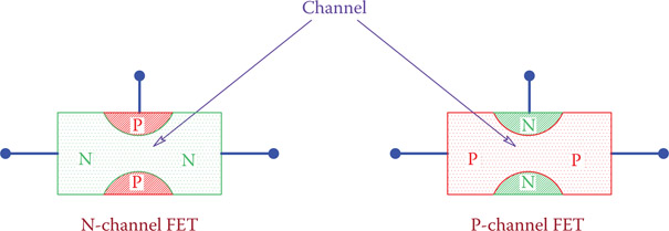
Figure 19.1
Schematic of FET active parts.
is very small, and all its elements are made on a body that itself is a semiconductor and is part of the transistor elements.
The three elements of a field effect transistor have names different than those for BJT. When a FET conducts, electrons move through the channel. One side of the channel is called the source (counterpart of emitter) and the other side is called the drain (counterpart to collector). The channel is physically surrounded by the opposite type semiconductor material, which can influence the extent (effective size) of the channel, thus introducing less or more resistance for the flow of electrons. This control action is carried out by the gate. The channel size (effect size not the physical size) is governed by the voltage applied to the gate (see Section 19.3) and not the current through the gate. This is why a FET is a voltage-driven device.
Source: (in semiconductors) One of the three terminals in a field effect transistor, comparable with the emitter in a junction transistor.
Drain: One of the three terminals in a field effect transistor (FET) counterpart of collector in a junction transistor.
Gate: Special connection in some semiconductor devices that upon receiving an appropriate signal (in the form of a voltage or pulse) allows controlling of the device, including turning it on and off.
There are many types of FETs and in some (with a symmetrical geometry for the channel) the designation of source and drain is governed by biasing (see Chapter 14 for biasing). In some others the channel does not have a symmetrical shape (structured different in the process of manufacturing) and one side of the channel is designated as the source and the other side is the drain. Figure 19.2 illustrates the schematic of the structure of a FET.
In comparison with a bipolar junction transistor the source, drain, and gate are the counterparts for emitter, collector, and base, respectively. Also, the N-channel FET is the counterpart of NPN transistor and the P-channel FET corresponds to a PNP transistor. Physically, FETs are made similar to BJTs, and there is no way to distinguish one from the other just by looking. One must pay attention to the name tag and the manufacturer’s data sheets.
Apart from a number of differences between these two categories of transistors, all that can be done by bipolar transistors, such as amplification, can also be done by FETs. In bipolar transistors we have common emitter, common base, and common collector amplifier. Likewise, in FETs we have common-source, common-gate, and common-drain amplifiers, respectively.
FETs can be used for amplification. Analogous to BJTs, it is possible to have common-source, common-drain, and common-gate amplifiers.

Figure 19.2
Schematic structure of FET.
In the same way that all discussions in Chapters 17 and 18 for an NPN transistor is equally applicable to a PNP transistor, whatever applies to an N-channel FET is true for a P-channel FET, too. The polarity of biasing and operating voltages, accordingly, are the reverse of each other for the N-channel and P-channel FETs. In what follows, we consider an N-channel field effect transistor.
FETs are voltage-controlled transistors.
19.3 FET Types
Field effect transistors are initially categorized into two types, junction field effect transistor and insulated gate field effect transistor. The first category is referred to by its abbreviation JFET. The second category is known as MOSFET because of the material used for its gate insulation being metal-oxide semiconductor. Thus, a more common name for the second category is metal-oxide semiconductor field effect transistor.
Junction field effect transistor: One type of field effect transistor (FET) in which the gate is not insulated. Those with insulated gates are more advanced and more common.
Insulated gate field effect transistor: Type of FET with insulated gate, like MOSFET.
Metal-oxide semiconductor: Type of semiconductor device in which metal oxide is used for insulation layers.
Metal-oxide semiconductor field effect transistor (MOSFET): Type of field effect transistor in which metal oxide (like SiO2) is employed for insulation of the gate.
The two types are different in structure and there is a difference between the way they can function. In JFET the isolation between gate and channel is a reverse biased PN junction. In MOSFET a layer of metal oxide is used for this purpose. This is schematically depicted in Figure 19.2.
In addition to the final categorization of each type to N-channel and P-channel, MOSFETs have subcategories, as discussed later. Figure 19.3 indicates the possible categories of field effect transistors. As can be seen, JFET family is associated with depletion, whereas MOSFET family is associated with depletion and enhancement. These (depletion and enhancement) are the modes of operation for each family; that is, the mechanism under which each category internally functions. They are described below.
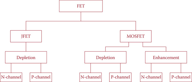
Figure 19.3
Tree of various families of field effect transistors.
Recall depletion from Chapter 14. In the depletion region around a P-N joint the electrons that have moved to this region reject and prevent other electrons to enter or pass through the depletion layer. This is what can happen in the channel of a FET. Suppose that the two sides of a channel formed by an N-type semiconductor are connected to a voltage, as shown in Figure 19.4. Electrons are attracted to the + side (from left to right). The channel material is a semiconductor, and it exhibits some resistance, behaving like a resistor. Consider three cases: (1) there is no voltage on the gate, (2) gate is connected to a negative voltage, and (3) gate is connected to a positive voltage.
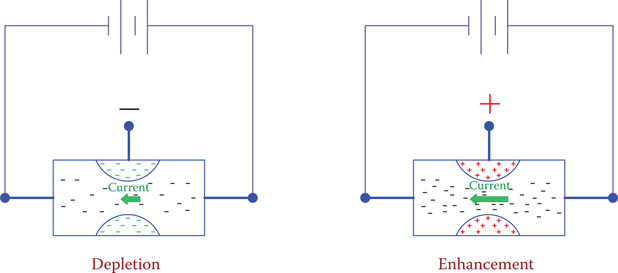
Figure 19.4
Depletion and enhancement in field effect transistor.
When there is no voltage on the gate, a current can flow in the channel due to the voltage difference between the two sides of the channel and based on the resistance of the channel. If now a negative voltage is connected to the gate, a negative field will be formed around the channel, as shown in Figure 19.4. The effect of this field is to reject electrons and decrease the current. This is the case called depletion because the negative field depletes the electrons in the channel. The stronger the field is, the lower the number of electrons passing.
When the gate is connected to a positive voltage, a positive field is formed around the channel. The effect on the electrons is to attract them and, as a result, help them move through the channel. This is called enhancement; the motion of electrons is enhanced. In both cases (depletion and enhancement) the stronger the field is the larger is the effect on the electron flow. As depicted in Figure 19.3, JFETs work only based on depletion, but MOSFETs can work either in the depletion mode or the enhancement mode.
Enhancement: One of the two methods to control the flow of electrons in the channel of a field effect transistor (FET).
In a FET, by changing the voltage on the gate the current between the source and drain can be controlled.
19.4 JFET
Although JFETs and MOSFETs are both field effect transistors, they have different symbols in the circuit schematics. The symbols for JFET and a comparison with their counterparts in bipolar junction transistors are shown in Figure 19.5.
For an N-channel JFET the drain voltage must be more positive than the source voltage; that is, the drain must be at a higher voltage with respect to the source. This is similar to the polarity for an NPN bipolar junction transistor where the collector-emitter junction must be forward biased. The gate for this type FET, nevertheless, must be negative with respect to the source; that is, the gate-source junction (P-type material in the gate and N type for the channel) must have reverse bias. The gate must have a lower voltage than the source. For this type of FET at the most the gate can be shorted to the source and have a voltage equal to that of the source. Gate voltage going more positive than the source voltage is harmful for the JFET and can damage it. For a P-channel JFET the reverse is true. Typical acceptable voltages are shown in Figure 19.6.
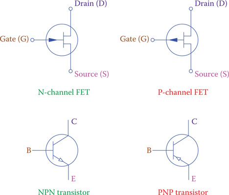
Figure 19.5
Symbols for N-channel and P-channel field effect transistors.
For N-channel JFET the gate must be negative with respect to the source.

Figure 19.6
Voltage and bias relationships for JFET: (a) N channel and (b) P channel.
In an N-channel JFET when a negative voltage is applied to the gate the effect is to introduce more resistance to the source-drain electric flow, as if the channel becomes narrower. This is due to the growth of the depletion region where the N-type and P-type materials meet. If the gate negative voltage is sufficiently high, then the channel entirely blocks and the current drops to zero. (The transistor goes to cutoff state.) In this respect, the highest source current corresponds to the case when the gate and the source have the same voltage.
Note that the gate-source junction is reverse biased. Consequently, there is no current flowing between the source and the gate. Unlike the case of a BJT, therefore, the source current and the drain current are the same. The voltage at the gate is only to maintain the electrostatic field around the channel. Similar to a BJT, various voltages and currents in a FET are denoted by their corresponding element. These are shown in Figure 19.7. These definitions are good for MOSFET, too.
The required bias condition exemplified in Figure 19.6 necessitates that both positive and negative voltages be available from a power supply. Having two power supplies is undesirable, and normally one power supply is used to power a transistor. In the same way as it was described in Chapter 18 for BJTs, appropriate biasing for FETs can be obtained by fix bias, self-bias or voltage divider bias. Their descriptions will not be repeated in this chapter, but they are shown in Figure 19.8. Example 19.1 helps to clarify the matter.
In a field effect transistor the source current and the drain current are equal.

Figure 19.7
Definition of FET circuit components.
Note that in the voltage divider biasing method the voltage at G is determined by the values of RG and R′G. This value is positive for a positive VDD. The voltage at S, however, is determined by the values of RS and IS. Correct gate-source bias can be obtained by choosing RSappropriately. Incorrect magnitude of RS can make the voltage at S smaller than the gate voltage (in an N-channel transistor), which can cutoff the FET; so, it is important that RS is correctly selected. When dealing with AC signals that cause IS to vary between a minimum and a maximum value, the transistor can go to cutoff for some values of IS.
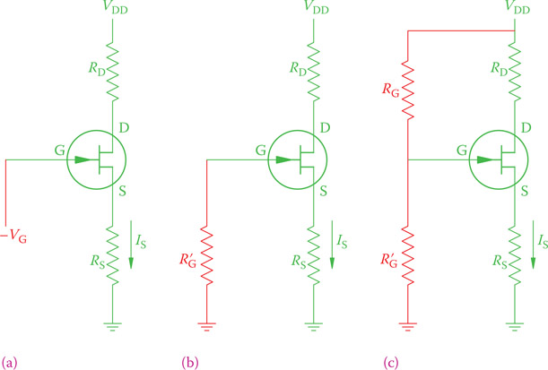
Figure 19.8
Biasing methods for FET: (a) fixed bias, (b) self-bias, and (c) voltage divider bias.
Example 19.1
In the transistor shown in Figure 19.9, what is the voltage difference between the gate and the source (VGS)?
Solution
The supply voltage is 20 V and the voltage at ground is 0. Because the current in the RS (470 Ω resistor) is 15 mA, there is a voltage drop of
(470)(0.015) = 7.05 ≅ 7 V
in the resistor. Thus, the voltage at S is 7 V.
Because the gate is connected to ground and there is no current in the 5.1 K resistor (because of the gate-source junction being reverse biased), the voltage at the gate remains zero. The source, therefore, is at +7 V with respect to the gate.
Example 19.2
In the circuit shown in Figure 19.8c the values of the various resistances are as follows: RD = 1.5 K, RS = 470 Ω, RG = 16 K, and R′G = 1.2 K. If the supply voltage is 24 V and the drain current is 10 mA, how much are the voltages VGS and VDS?
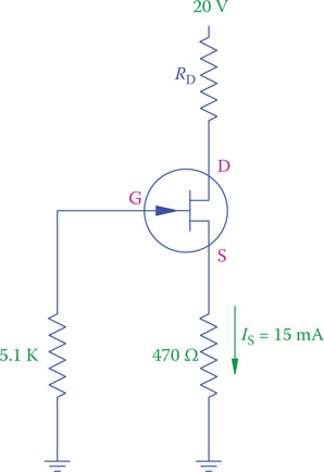
Figure 19.9
Circuit of Example 19.1.
Solution
Voltage at gate can be found from voltage divider relationship
Source current is the same as the drain current. The voltage at S can then be found from the voltage drop in RS
VS = (470)(0.010) = 4.7 V
The source-gate voltage, thus, is
VGS = VG − VS = 1.7 − 4.7 = −3 V
The drains-source voltage can be found from the difference between the supply voltage and the voltage drops in RD and RS:
VDS = 24 − (1500 + 470)(0.010) = 4.3 V
19.5 MOSFET
The metal oxide semiconductor field effect transistor (MOSFET) is a FET whose gate is insulated from the main body of the transistor by a layer of metal oxide semiconductor (such as SiO2). This layer is very thin, and for this reason MOSFETs are prone to get damaged easily if they are subject to voltages higher than their ratings. They are also very sensitive to static electricity, and they must be handled with care and sufficient protection from receiving static electricity in order not to get damaged.
In addition to the gate being insulated, one more difference between JFET and MOSFET is the channel. While in a JFET, the channel is made of the same material as the source and drain, a MOSFET has no channel, or has a smaller channel made of a semiconductor material that is much less doped than those of the source and drain.
As pointed out earlier, there are two types of MOSFET based on the mechanism that they function, depletion and enhancement. The first type is called D-MOSFET. It has a channel, and it can work both in depletion and enhancement mode (for this reason sometime it is called DE-MOSFET). The second type, called E-MOSFET, can only work in the enhancement mode. Figure 19.10 schematically depicts the structural difference between the two types.
An E-MOSFET is an off device, meaning that when no voltage is applied to the gate (VGS = 0), the transistor is in the cutoff mode. If then a positive voltage is applied to the gate, it develops a current between the source and the drain. This current can be controlled by changing the gate voltage. In the D-MOSFET, however, there is a current IDS between the drain and source even when VGS = 0 (when a VDS exists between the drain and the source). Then IDS can be lowered (working in the depletion mode) by having a negative voltage applied to the gate or it can be increased (working in the enhancement mode) by applying a positive voltage to the gate.
Symbols for the main categories of MOSFETs are shown in Figure 19.11. There are more varieties of MOSFET, but we do not consider them here.
A MOSFET has a high input impedance (see Section 18.8 for input impedance). This is a definite advantage over the BJT and JFET because it implies low input current and very low power dissipation. Also, it is more appropriate for connecting to devices with a high output impedance. Other advantages that have made the use of MOSFETs more popular than BJTs are (1) insensitivity to temperature change and (2) high-frequency capability (fast switching).

Figure 19.10
Structural difference between D-MOSFET and E-MOSFET.

Figure 19.11
MOSFET symbols.
Considering the first issue as an advantage is very obvious. Transistors can become unstable when the operating temperature rises in a device. The second issue is very important for operation on high-frequency signals (e.g., in telecommunications). It is required that a device turns on and off with a desired (normally very high) frequency. A bipolar junction transistor cannot perform this switching at very high frequencies. Despite these advantages, MOSFETs have limitations on the voltage and power that they can handle. Typical maximum values can be said to be 250 V and 500 W.
19.6 Testing a MOSFET
A MOSFET can get damaged in two ways, the insulation of the gate breaks or the gate shorts to the channel. In either case the MOSFET cannot function as expected. In handling a MOSFET, extra care must always be taken not to cause any voltage contact to the terminals and that the terminals do not touch any material that can generate or contain static electricity. In testing a MOSFET the same precaution is necessary.
Testing a MOSFET mainly consists of measuring the resistance between its source and drain. When a MOSFET is conducting, this resistance is lower than when it is in cutoff. In this sense, for the conducting condition, its resistance must be much smaller than for no conducting condition, for which the resistance is very high.
A MOSFET can be tested either by an ohmmeter or by the diode test setting of a digital multimeter (DMM). If an analog ohmmeter is used, it must be put on the 100 K range. Two tests are done, one with the gate field existing and one with the gate field absent. In the presence of the gate field the meter reading indicates some value for the channel resistance, and in the absence of this field the channel resistance is very high. It is necessary first to identify the drain, gate, and source for a MOSFET to be tested.
To test an N-channel MOSFET, connect the black lead of the ohmmeter or DMM to the source of the MOSFET without touching the terminal pins by hand. Then with the red lead touch the gate. This creates the gate field. Move the red lead to the drain, and the meter should read some small value (the needle of an analog meter should move to the midrange).
Now, if without disconnecting any of the two leads touch a finger between the gate and source pins (to discharge the field through your fingers), the MOSFET goes to nonconducting condition and the meter reading goes high; that is, in an analog meter the needle stays on the left, and a DMM shows OL. The above observation is for a good MOSFET. If in both cases the needle moves to the right end (zero ohm) or the DMM shows a near zero value, the device is shorted and damaged.
19.7 Insulated Gate Bipolar Transistor
An insulated gate bipolar transistor (IGBT) is a transistor similar to a BJT but with more and improved capabilities such as fast switching. It is now widely used in many switching devices and vastly used in power converters (particularly in wind turbines), as we discuss in Chapter 20. As the name implies, IGBT has a gate and the gate is insulated from the body. This allows high voltage and high current in the IGBT to be isolated from the control signal to the gate.
Insulated gate bipolar transistor (IGBT): Type of gated transistor used in power converters. Its gate is insulated and is connected to a much smaller voltage to turn the transistor on.
Whereas a BJT is a current-driven device, an IGBT has a gate and it is a voltage-controlled device. This is much desirable and preferred, similar to a MOSFET. This means it has the advantages of high-current handling capability of a bipolar transistor with the ease of control of a MOSFET.
In comparison with a BJT, an IGBT has a collector and an emitter, but a gate instead of a base. The structure of an IGBT is a combination of a BJT and a MOSFET. From the structure viewpoint, there are two types of IGBTs, PT, and NPT, which stand for punch through and nonpunch through. These are schematically shown in Figure 19.12. The difference is in the additional layer in the PT type IGBT. In fact, an IGBT works as a combination of a BJT and a FET, but we do not go to its details.
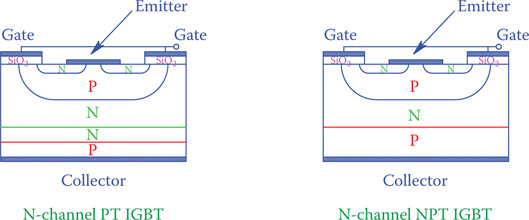
Figure 19.12
Structure schematics of IGBT.
The symbol for an IGBT is shown in Figure 19.13. There are two different symbols. Either symbol can be used. Figure 19.14 depicts two 1200 V, 600 A IGBTs. They have an embedded controller for overcurrent and overtemperature protection.

Figure 19.13
IGBT symbols. Two symbols for either N-channel or P-channel IGBT.
As will be discussed in Chapter 21, IGBTs are used as switching devices. For an N-channel IGBT the collector-emitter current can be turned on and off by placing a positive voltage on the gate. As long as there is a forward bias potential difference between the collector and the emitter, a positive voltage on the gate turns the transistor on.
After an IGBT is turned on, it then can be turned off by either removing the positive charge on the gate (introducing a negative or zero voltage to it) or removing the VCE (supply voltage). When connected to AC, if the IGBT is turned on, after half a cycle it will turn off, because this includes reverse biasing the collector-emitter junction.
In operation an IGBT becomes very warm. Cooling by water may become necessary. Figure 19.15 shows an IGBT in the control system of a 1.5 MW wind turbine. The two hoses on the right are for circulating water to take the heat away.

Figure 19.14
Examples of IGBTs.
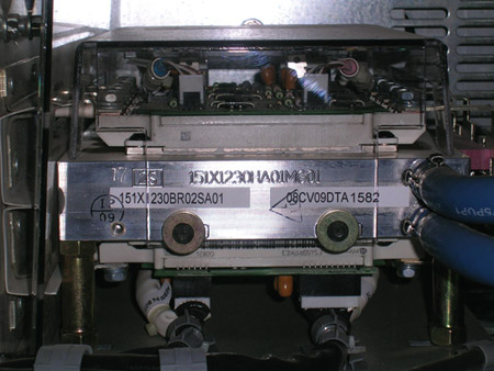
Figure 19.15
Example of IGBTs inside a circuit, cooled by water circulation.
19.8 Thyristor
Similar to other electronic devices discussed so far, a thyristor is frequently used in electronic appliances, including the electronics for control devices in renewable energy technology. Thyristors are, in fact, a family of about 24 devices, but we are more interested in those that behave like a diode (rectifies electric current). The advantage of a thyristor over a diode is that its function can be turned on and off. Thus, it functions as a switchable diode. For this reason it is also called silicon-controlled rectifier (SCR). It is a rectifier whose functioning is electronically controlled.
Thyristor: Gated semiconductor device whose conduction can be controlled by a pulse sent to its gate. It is used in power converters.
Silicon-controlled rectifier (SCR): A family of gated diodes or transistors that can be controlled (turned on and off) through their gates.
Structurally, a thyristor is made of two internally connected transistors, but it can be regarded as a transistor with an extra junction, as shown in Figure 19.16. However, it is employed as a diode and the extra junctions are for its control. Thus, it has three elements, the anode, the cathode, and the gate. Figure 19.16 depicts also the symbol of a thyristor.
In practice, a thyristor is comparable with an IGBT when used for switching. They are interchangeable when the current and voltage rating are compatible, and their required switching frequency allows. A main difference in their operation, however, is as follows.
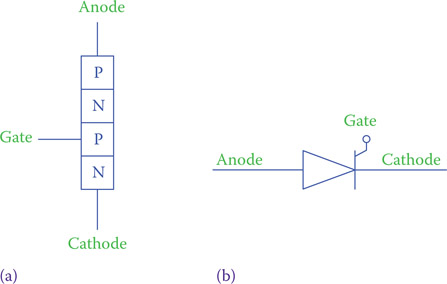
Figure 19.16
(a) Thyristor construction and (b) thyristor symbol.
An IGBT is turned on by applying a voltage to its gate. As long as the voltage is on the gate, provided that correct bias exists between collector and emitter, the IGBT keeps conducting.
A thyristor is turned on by sending a positive pulse (short duration voltage) to its gate. It keeps conducting as long as the forward bias voltage difference between its anode and cathode exists (it is not necessary to repeatedly update the pulse), and there is a current. If the current ceases for any reason, the thyristor turns off, and to turn it back on, another pulse to the gate is necessary. A thyristor can also be turned off by reversing the polarity of the voltage applied between its anode and cathode. This is what happens naturally when a thyristor is used as a rectifier. After a positive half cycle current is followed by a negative current, a thyristor stops conducting. This is further discussed in Chapter 20 (see Section 20.3).
The action that takes place in a thyristor, that when it is turned on it keeps conduction though the activating signal (to the gate) has ceased, is called “latching.” This is a desirable property in some applications. A pulse with the correct voltage can start a process, and it is not necessary to maintain the voltage (like in the case of an IGBT). For some other applications, as we will see in Chapter 20, this is an undesirable feature because there is no control on stopping the device. For this reason, some thyristors are equipped with additional capability that they can be turned off when desired by sending a negative pulse to their gate. Among these we only name two, the gate turn off (GTO) thyristor and integrated gate-commutated thyristor (IGCT).
Gate turn off (GTO) thyristor: Type of thyristor with the capability that can be turned off by sending a negative voltage pulse to its gate, also called GTO thyristor, as opposed to those without this extra capability (they turn off as the applied voltage becomes negative).
Integrated gate-commutated thyristor (IGCT): Class of “gate turn off thyristor,” in which its gate and antiparallel diodes are integrated with it in a package.
The action of turning off a thyristor or a similar device in a circuit is referred to as commutation. If this is done by the circuit itself, as when current direction can reverse, it is called natural commutation, and when it is done by an external circuitry to send a signal to the gate or turn the device off by other means, it is called forced commutation.
Natural commutation: Act of automatically turning off in a gated diode or transistor (a thyristor) when an alternating current applied across its main terminals changes direction (goes to negative half cycle). This is the opposite of “forced commutation” where the device is turned off through a control signal to its gate.
Forced commutation: Turning off a thyristor by applying a negative voltage to its gate, as opposed to natural commutation in which a thyristor turns off as the alternating current applied to it reaches its negative half cycle.
A thyristor is turned on by sending a positive pulse to its gate.
19.9 Chapter Summary
- The principal structure of a field effect transistor is a channel made of a semiconductor material surrounded by the opposite semiconductor material.
- The three terminals of a FET are called source, drain, and gate.
- In operation, electrons move inside the channel between the source and the drain while affected by an electrostatic field generated and controlled by the gate voltage.
- There are two families of field effect transistors, JFET and MOSFET.
- JFET stands for junction field effect transistor. MOSFET stands for metal oxide semiconductor field effect transistor.
- FETs are voltage-driven devices. The gate voltage controls the drain-source current.
- FETs can be either N channel or P channel.
- A bipolar junction transistor (BJT) can handle higher currents and higher voltages than a FET.
- The source, drain, and gate in a FET correspond to the emitter, collector, and base in a BJT.
- A FET is faster than a BJT and is more suitable for higher-frequency switching.
- A BJT consumes more power than a FET.
- There are two types of MOSFET: D-MOSFET and E-MOSFET.
- A FET like a BJT can be used for amplification and switching.
- IGBT stands for insulated gate bipolar transistor.
- IGBT is a bipolar junction transistor with a gate. It has a collector, an emitter, and a gate.
- SCR stands for silicon-controlled rectifier.
- SCR is the most common member of thyristor family. It is common to use the name thyristor when addressing SCRs.
- A thyristor behaves as a diode with a control gate.
- For switching, an IGBT and a thyristor can be interchanged (if their operating properties permit).
- An IGBT needs a continuous voltage on the gate to keep conducting.
- A thyristor turns on with a positive pulse; then it latches and keeps conducting.
- There are many members in the thyristor family; some can be turned off by a negative pulse sent to the gate, addressed as gate turn off or GTO.
Review Questions
- What does FET stand for?
- What is the reason for the name FET?
- What are the three elements of a FET?
- What are the counterparts of a BJT base, collector, and emitter in a FET?
- What is the structural difference between a JFET and a MOSFET?
- What does a gate do in a FET?
- Describe two differences between the structures of a BJT and a FET.
- Describe two differences between the characteristics of a BJT and a FET.
- Name three ways that a FET can be biased.
- What is the difference between an N-channel and a P-channel FET?
- What is/are the difference(s) between D-MOSFET and E-MOSFET?
- What does SCR stand for?
- What does IGBT stand for?
- What is a thyristor?
- What is the relationship between a thyristor and a SCR?
- What is an IGBT used for?
- What is a SCR used for?
- What is the difference between an IGBT and an IGCT?
Problems
- In Figure P19.1, find the voltage VGS.
- If the source current varies in Figure P19.2, what is the minimum acceptable current in the source that does not violate the bias condition?
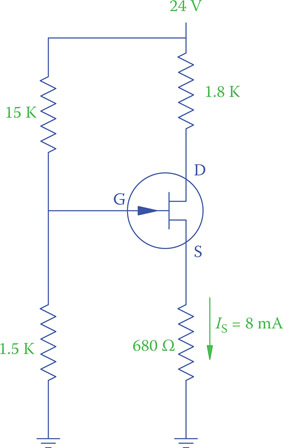
Figure P19.1 Problem 1 circuit.

Figure P19.2 Problem 2 circuit.