
20
Power Converters
OBJECTIVES: After studying this chapter, you will be able to
- Describe what an inverter is
- Make a single-phase square-wave inverter
- Understand a three-phase inverter
- Define terms such as firing angle and freewheel diode and their purposes
- Describe how output of a rectifier is controlled
- Describe how output of an inverter is controlled
- Explain what a power converter is
- Describe the structure of a thyristor-based converter
- Explain how a converter can be used as a rectifier or as an inverter
- Define pulse width modulation
- Define what pulse width modulation can be used for
- Understand single-phase and three-phase use of inverters based on PWM
- Define amplitude and frequency modulation ratios
New terms: Amplitude modulation ratio, carrier, converter, driver, firing angle, freewheel diode, freewheeling diode, frequency modulation ratio, inverter, overmodulation, photovoltaic (PV) system, pulse width modulation (PWM)
20.1 Introduction
In Chapter 16 we discussed rectifiers, both single phase and three phase: they convert AC to DC. We also learned that diodes are the principal element of any rectifier and that we can use them as half-wave, full-wave, and bridge rectifiers.
The material in this chapter is a continuation of the same framework of devices. First, an inverter is introduced. An inverter does the opposite task of a rectifier and provides an AC waveform from a DC source. Then we continue with replacing a diode in a rectifier by a switchable device; we discussed this in Chapter 19. This allows controlling the output voltage of a rectifier. For rectifiers we focus only on three-phase systems, as in industry three-phase devices are used more frequently than single-phase devices, which are normally small.
Next we discuss three-phase inverters, and we see how the same structure can be used for both rectification and inversion. This is why the term converter is employed, referring to both a rectifier and an inverter.
Converter: General term for a rectifier (a device that converts AC to DC) and an inverter (a device that converts DC to AC).
We recall that the output of a rectifier contains ripples, and, to eliminate or reduce the ripples, filters are employed. The same thing is true for the converters, and filters are used in order to smooth the output of a rectifier constructed from switching devices. The discussion about filters is not repeated, and one can use all that was already discussed (see Section 16.5) for the devices explained in this chapter.
Power convertor refers to both rectifier and inverter.
20.2 Inverter
The name inverter is used for a device that converts DC to AC; that is, the opposite function of a rectifier. This is the way to provide AC from a battery for the devices that work with AC. For instance, if one wants to use a TV or a razor that works with 110 V AC, and the only available electricity source is a 12 V battery, an inverter becomes necessary. It is necessary that the generated AC electricity has both the required voltage and the required frequency. In the example of using a 12 V battery to generate 110 V AC, thus, using a transformer to increase the AC voltage becomes necessary. The reverse operation (changing from a higher voltage to a lower voltage) does not need a transformer.
Inverter: Electronic device that generates AC electricity from DC. In the simplest form the generated AC is square wave.
Inverters can provide both single-phase and three-phase AC. In both cases, there is only one DC power supply (it is not necessary to have three batteries for three-phase AC conversion). First, we consider the single-phase inverter.
20.2.1 Single-Phase Inverter
Obtaining AC from DC is based on switching the direction of current in a load. This is only possible with power electronic devices that can be controlled, i.e., those whose function can be turned on and off. These are devices such as a thyristor and an insulated gate bipolar transistor (IGBT) that we discussed in Chapter 19. The controls must also allow choosing the voltage and frequency of the generated AC signal as desired. The timing for the switching action, therefore, is quite important. In the simplest form, the output of an inverter is a square-wave AC signal, and not a sinusoidal waveform.

Figure 20.1
Arrangement for a single-phase inverter.
Figure 20.1 shows the schematics of the arrangement for a single-phase inverter. There are four switching devices to control the direction of current at each instant. These can be thyristors or gated transistors (e.g., IGBTs). For the sake of simplicity in the rest of this chapter they are only referred to as thyristors. Each of the four thyristors in the circuit allows current in only one direction and only when it is turned on through its gate. At all other times it blocks the current in either direction because of being reverse biased or turned off. These thyristors are turned on and off in an orderly manner and with an appropriate sequence and a desired frequency. The thyristors are divided into two pairs connected between the positive and negative terminals of the power supply, and the load is connected between the two pairs. The thyristors are numbered 1 to 4 for ease of reference.
Consider if with a frequency of 100 Hz sequentially thyristors T1 and T2 are turned on together, then turned off, immediately followed by turning on thyristors T3 and T4 together and then off together, with the same sequence repeated. The duration each time a pair of thyristors is on, is therefore 1/100th of a second. The result, as observed by the load, is a square-wave alternating current with 50 Hz frequency and a voltage very near the voltage of the DC power supply (three is a small voltage drop in the electronic parts). This is the way that an inverter works.
Note that the two thyristors on the same leg (e.g., T1 and T4 or T2 and T3) should never be on at the same time because they short the power supply and damage it. Also, in operation, each pair that is on must be turned off before the other pair is turned on. For the action of turning the thyristors on and off, a separate electronic circuit is necessary. This circuit is normally called driver. The driver circuit must take care of the timing and frequency of turning the thyristors on and off.
In an inverter, the two thyristors in the same leg should never be in the on state at the same time.
Driver: Circuit to turn on and off the gates of gated transistors and similar devices in applications that require an orderly action of one or more of these devices.

Figure 20.2
Freewheel diodes to protect the circuit from overvoltage.
If the load is purely resistive, then the current in the load will have the same pattern of the AC voltage, which is a square wave. For inductive and capacitive loads, as we discussed in Chapter 8, because of the charging effect of capacitor and the Lenz’s law in the inductor, the current and voltage are not in phase and some large voltages may develop in part of the circuit. To prevent damage because of these voltages, usually parallel with each thyristor there is a diode allowing current in the opposite direction, as shown in Figure 20.2. The role of the diode is to make a path for current to flow and prevent a voltage buildup. These diodes are called freewheel diode, or freewheeling diode. Note that these diodes are reverse biased.
Freewheel diode: Diodes put antiparallel to a gated diode (thyristor) in a converter to make a reverse path for current and prevent buildup voltage across the thyristor.
Freewheeling diode: Same as freewheel diode.
Thus, they do not short the power supply and do not conduct in the normal conditions.
The inverter as stated, having zero interval between the time a thyristor is turned off and the associated thyristor in the same leg is turned on, generates a square AC waveform as shown in Figure 20.3a. However, if a short interval exists between the two actions (turning off a thyristor and turning on its pair) the generated waveform assumes a different shape, as illustrated in Figure 20.3c. This figure corresponds to the case where there exists a delay of T2 between the instant one set of thyristors are turned off (after being in the on state for a period of T1), and the instant the other set are turned on. Thus, for a period of T2 all the thyristors are turned off.
As can be seen the total period for one cycle of the AC waveform is 2(T1 + T2). Thus, the frequency of the resulting alternating current is = =12(T1+T2)

Figure 20.3
Current waveforms for an inductive load based on output voltage. (a) Voltage pattern in a square waveform. (b) Current in an inductive load with a square wave. (c) Square waveform with delay. (d) Current in an inductive load subject to voltage shown in (c).
Although the current variation in a pure resistive load is the same as the voltage, for a different type of load the current variation is different than that of the voltage, as dictated by the load. For instance, for an inductive load the current does not have a square-wave pattern, It rather looks like the waveforms in Figure 20.3b and 20.3d for the voltage waveforms in Figure 20.3a and 20.3c, respectively. As can be seen, the current in an inductive load has a form closer to a sine wave than a square wave.
By changing the time intervals T1 and T2 it is possible to change the current waveform to some extent, as can be seen from Figure 20.3d. It is customary to represent T1 and T2 in terms of angles. In such a case they do not associate with frequency anymore but can indicate the percentage of time in each cycle that a thyristor is on. For this, T1 + T2 = 180°, and if, for instance, T1 = 120° and T2 = 60°, it implies that each set of thyristors are on for 120° and stay off for the rest of a cycle (i.e., for 60° + 180° = 240°). In practice, the driver circuit (software and/or hardware) that controls the thyristors takes care of frequency by repeating the cycle after an elapsed time.
The best result, as far as having an output as close as possible to a sinusoidal waveform is concerned, is when T1 = 133.5° and T2 = 46.5°.
To improve the quality of the output waveform from an inverter, so that it better resembles a sinusoidal waveform, various techniques are available. One of these is pulse width modulation, which is separately discussed later (see Section 20.6). Another technique is to increase the switching steps and accordingly the necessary controls to generate stepping signals as illustrated in Figure 20.4.
Obviously, the more steps there are, the more costly the device. The steps in the configuration in Figure 20.4 have the same width (time duration). Figure 20.5 shows how a step waveform can be obtained from combining inverters with different outputs of the form in Figure 20.3c.
Practically, a waveform shown in Figure 20.5b can be made by adding the outputs of two inverters together. One way for this is indicated in Figure 20.6, where the outputs of the inverters are added together through a transformer.
The term firing is normally used for turning a thyristor on. Also, firing angle represents the delay from the start of a cycle, normally in terms of degrees, when a thyristor must be turned on. For instance, in Figure 20.5 the firing angle for the inverter to generate signal A is 22.5° and for the
Firing angle: Delay from the beginning of a cycle of an AC signal for voltage control in a converter. Delay determines when the gated devices in the converter become active and, thus, the percentage of the 360° cycle that the AC waveform is ineffective.
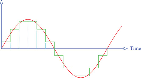
Figure 20.4
A 12-step waveform.
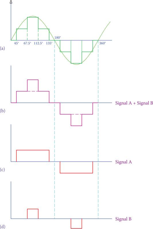
Figure 20.5
A step waveform made up of combining simpler waveforms. (a) Two-step sine form approximation. (b) Two-step waveform made up of two square waves A and B. (c) Square wave A. (d) Square wave B.

Figure 20.6
Adding two waveforms together through a transformer. A practical way of adding two square waves.
inverter to generate signal B is 67.5°. In this sense, the two inverters in Figure 20.6 can be similar but have different firing schemes.
20.3 Thyristor-Based Three-Phase Rectifier
In Chapter 16 we discussed three-phase rectifiers constructed with diodes (see Section 16.6). The rectifier shown in Figure 16.11 was a three-phase bridge rectifier that uses six diodes. This is sometimes called full-wave bridge rectifier as compared to a three-phase half-wave rectifier with only three diodes. Because at the industrial level a six-diode rectifier is used more commonly, we leave out the description of three-phase half-wave rectifier.
The discussion in this chapter for three-phase converters heavily relates to the diode-based rectifiers already discussed. Thus, we first restate certain details that have been left out for this chapter.
20.3.1 Revisiting Diode-Based Three-Phase Rectifiers
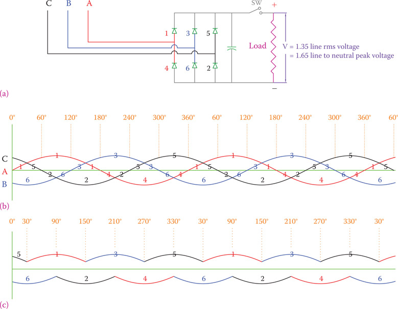
Figure 20.7
A three-phase bridge rectifier employing six diodes. (a) Schematics of a 3-phase rectifier. (b) Waveforms of the individual three phases. (c) Voltage of the DC from rectifier based on conduction of diodes.
A three-phase diode rectifier is shown in Figure 20.7a. This is the same as was depicted in Figure 16.11a, except that the diodes have been numbered. Diodes 1 and 4 are on phase A, 3 and 6 are on phase B, and 5 and 2 are on phase C. The upper diodes (1, 3, and 5) conduct when the corresponding phase is going through its positive half cycle, and the lower diodes (4, 6, and 2) conduct during the negative half cycle.
Figure 20.7b illustrates the diode numbers corresponding to each phase for each 60° interval, based on their phase and its polarity. As mentioned earlier (see Section 16.6), a diode does not conduct for the whole duration of a half cycle it is forward biased by its line voltage. At each instant, only the two diodes corresponding to the most positive voltage and the most negative voltage conduct and supply the highest possible voltage difference across the load. For example, during the interval between 0 and 30°, in each 360° cycle as represented in Figure 20.7b, diode 5 has a higher voltage than diode 1, while both A and C phases are at their positive cycle. During this period, on the basis of the voltages present at its terminals, diode 1 is reverse biased and does not conduct. The condition reverses for the period between 30° and 60°, where phase A dominates and diode 5 does not conduct.
Figure 20.7c shows the most positive and most negative voltages for two cycles of the AC line as well as the numbers for the conducting diodes at various instants during these cycles. This figure clearly shows which diodes are conducting at each interval. Take notice of the important fact that each diode conducts for 120° during its line cycle and turns off for the rest 240°.
It is customary to use a chart similar to Figure 20.8 to show the on state of each diode with respect to other diodes. This chart is more useful when switchable devices are used instead of diodes; in particular, it shows the instant when each device is turned on and starts conducting. For each diode the hatched area shows the start and end of conduction. The chart also shows which two diodes are on at each instant.

Figure 20.8
Timing chart for conducting diodes in the three-phase rectifier of Figure 20.7.
Notice the sequence the diodes start conducting, being 1, 2, 3, 4, 5, and 6. It can be seen from both Figures 20.7c and 20.8 that the functions of diodes switch after an interval of 60°, and one pair of diodes conduct for each interval. Switching action takes place automatically based on the voltage variation in the three lines, and the conducting pairs and their switching order are 1&2, 2&3, 3&4, 4&5, 5&6, and 6&1, repeated. This order also illustrates the reason why the diodes in Figure 20.7 are numbered this way.
20.3.2 Substituting Diodes by Switchable Devices for Three-Phase Rectifiers
As we have discussed, it is possible to use switchable devices such as thyristors and IGBTs instead of diodes. When switchable devices are employed, it becomes necessary to fire each device repeatedly and continuously as far as it is expected to operate. If a thyristor is not fired, then no rectification takes place, and there is no output. This firing or triggering must be based on a proper triggering scheme. For a rectifier, firing of each thyristor must take place in a timely manner and only during the half cycle when it is forward biased. In the rest of this chapter for simplicity we only use the word thyristor where it is meant to refer to a switchable device, which can be a thyristor or an IGBT.
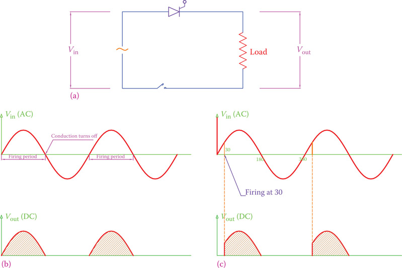
Figure 20.9
Output of a thyristor subject to alternating current and triggered with different firing angles. (a) Thyristor circuit. (b) Firing angle = 0. (c) Firing angle = 30∘.
Figure 20.9 shows the performance of a thyristor when subject to an alternating current (two cycles are shown). If triggering occurs exactly at the zero crossing point (the instant of zero voltage) for negative to positive voltage, the thyristor starts conducting at that moment and continues to conduct as far as it is forward biased. After a current is established, the device turns off by itself as the applied AC proceeds to its negative half cycle. At the moment of zero crossing from positive voltage to negative, the voltage across the thyristor changes sign and the device becomes reverse biased. Consequently, the current drops to zero. The resulting DC output is shown by the hatched area in Figure 20.9b.
Figure 20.9, furthermore, illustrates what happens if thyristor firing does not take place exactly at the zero crossing point but with a delay. In this case the rectified signal has duration of less than half cycle of the applied AC signal. The case is depicted by the hatched area in Figure 20.9c for a 30° firing angle.
Figure 20.10 illustrates a full-wave three-phase rectifier employing six thyristors numbered T1 to T6, following the same numbering method as in Figure 20.7.
This rectifier has a structure and performance similar to that in Figure 20.7, except that it needs a driver to send firing signals to the gate of each thyristor to turn it on. The triggering must be sequential and based on a scheme like that shown in Figure 20.8. The thyristor driver timing must be synchronized by the time of zero crossing of one of the three phases, which is also the instant that the other two phases have the same magnitude, but opposite sign.
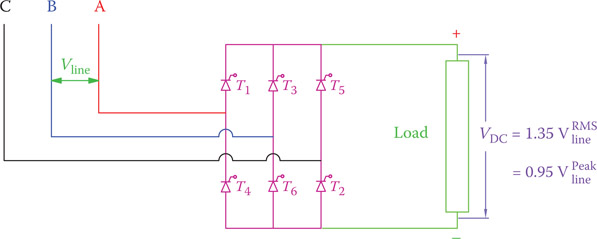
Figure 20.10
A three-phase bridge rectifier employing six thyristors.

Figure 20.11
Gate firing scheme for a three-phase rectifier.
Figure 20.11 shows the firing sequence of thyristors, starting from T1 in the upper leg of phase A. After each 60° of the AC sine wave a thyristor that is already on must turn off and another one start. This is shown in Figure 20.11 for some instances. Turning off is done naturally by the voltage change across each thyristor creating a reverse bias condition.
DC voltage obtained from the above three-phase rectifier is
| VDC=0.95(Vline)Peak=1.35 Vline | (20.1) |
Thus, for 208 V, line voltage VDC = 280 V, and for 380 V line voltage, VDC = 513 V.
Note that this value is the maximum voltage that can be obtained. In practice, we may want a lower voltage. In such a case the output voltage can be controlled, as discussed next.
20.3.3 Voltage Control in Thyristor-Based Rectifier
One of the advantages of using switchable devices instead of diodes in a rectifier is the possibility to control the voltage of the DC output. This is done by introducing a delay in the firing of all thyristors. This delay, normally expressed in terms of an angle and measured in degrees, is defined as the firing angle (the same term we have already seen for the single-phase inverter). All thyristors must have the same delay in their triggering.
When there is a delay in triggering thyristors, those ones that should turn off were there no delays (because of receiving a voltage at their cathodes that changes their bias condition) continue to conduct. For instance, in Figure 20.12, assuming no triggering delay, T1 starts conducting at point L and continues until point M when T3 is triggered and caused T1 to turn off. But, if T3 is not triggered, then T1 stays on. During the interval between M and N, if T3 is triggered, it turns off T1; otherwise, T1 conducts until N. At point N it turns off naturally (natural commutation; see Section 19.8) and stops conducting. It starts conducting again afterward, whenever its gate receives a positive pulse, while it is forward biased. Likewise, if thyristor T2 is not started at point P, then T6 does not turn off and conducts until the time point Q is reached.
Note that all preceding statements are true when the load is purely resistive. In cases of inductive and capacitive loads the conditions change. A detailed study of what happens in various conditions is outside the scope of this book.

Figure 20.12
On and off conditions of a thyristor.
Figure 20.13 illustrates the case when the firing angle is not zero. The firing times and thyristor states (on or off) can be compared for three cases when the firing angle is 0, 30°, and 50°. Figure 20.13a corresponds to zero firing angle. It also shows the two thyristors that conduct for each 60° interval. For example, at the start of the period between 0 and 60°, T1 was triggered and T6 was already on and continued to conduct. When there is a delay in firing, then all thyristors are triggered by the same nonzero firing angle, meaning that still the same pair of thyristors as in the case of no delay conduct simultaneously. In other words, the conducting interval that each pair of thyristors share is shifted in time. In Figure 20.13b and 20.13c the delay is represented by α (alpha), which is 30° and 50°, respectively.
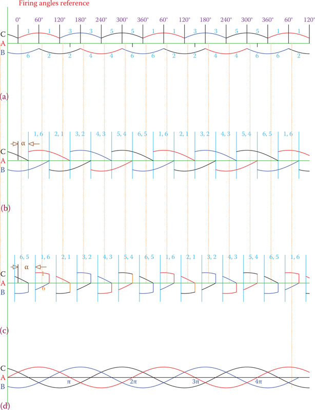
Figure 20.13
Comparison of DC output with (a) 0, (b) 30°, and (c) 50° firing angle and (d) input AC.
For certain firing angles at time intervals when one of the thyristors in a pair turns off by natural commutation, only one thyristor conducts, and, therefore, there is no voltage across the load and no current in it. This is especially true for resistive loads because electricity cannot be stored in them. This has happened for the 50° firing angle in Figure 20.13. It is the reason for the blank intervals in the output DC voltage, shown in Figure 20.14c. Figure 20.14 is a complement to Figure 20.13, showing the DC output voltages and their average values for the three different firing angles.

Figure 20.14
Showing examples of the DC output and its ripple. (a) 0, (b) 30°, and (c) 50° firing angle.
The result of a delay in triggering thyristors in a rectifier is the reduction of the output voltage. As can be seen from Figures 20.13 and 20.14, the average output voltage becomes smaller as the firing angle is increased. In this way the output of a thyristor-based rectifier can be controlled, as desired, by adjusting the firing angle. The output voltage is proportional to the cosine of the firing angle. If the firing angle is represented by α, then we can write
| VDC=VDC0cos α=1.35 Vlinecos α | (20.2) |
In Equation 20.2, VDC0 represents the DC voltage from the rectifier when α = 0. Equation 20.2 also implies that if α = 90°, there is no DC output (VDC = 0).
Figure 20.14 also depicts the DC output of the two aforementioned firing angles compared with that of zero firing angle. It is evident from the figure that the ripple frequency is the same (6 times the line frequency), but the ripple percentage gets larger as the firing angle increases.
Output voltage from a rectifier can be adjusted by altering the firing angle of its thyristors.
20.4 Thyristor-Based Three-Phase Inverter
Single-phase inverters are good only for small appliances. At the industrial level, such as for motor drives, HVDC, solar energy from photovoltaic (PV) systems variable speed wind turbines and turbines equipped with doubly fed induction generator (DFIG), three-phase inverters are widely used. These inverters use thyristors and IGBTs. As mentioned before, thyristor in our discussion implies an electronically controllable switchable device.
Photovoltaic (PV) system: A setup of photovoltaic panels to absorb solar energy. Photovoltaic panels are made of an array of solar cells connected together (in series and parallel) for a desired voltage and a desired current. A solar cell is a semiconductor that converts light to voltage, that is, generates a voltage across its terminals proportional to the light it receives.
The simplest three-phase inverter uses six thyristors and has a structure as shown in Figure 20.15. This configuration is called six-step inverter. The drivers for turning the thyristors on and off are not shown. Each thyristor has a freewheel diode in parallel with it but with the opposite polarity (direction) to protect it from high voltages that can develop in the circuit. As in the case of single-phase inverter, the two thyristors on the same leg cannot conduct at the same time; otherwise, they make a short circuit across the power supply.
20.4.1 180° Conduction
Thyristors must be triggered sequentially on the basis of a specific scheme so that the voltages appearing in A, B, and C have a good resemblance to a three-phase alternating current with 120° phase difference between each two phases. In the triggering scheme in Figure 20.16, each thyristor is in the on state and conducts for 180°, followed by 180° in the off state. The time for this period (i.e., the time for retriggering the same thyristor) defines the frequency of the generated alternating current. For instance, if each thyristor is fired every 20 msec, then the frequency of the output AC is 1 ÷ 0.020 = 50 Hz. In this respect, for a frequency of 60 Hz, if this firing scheme is used, then each thyristor must be fired every 1 ÷ 60 = 0.01667 sec, or 16.67 msec.

Figure 20.15
Schematic of a three-phase six-step inverter circuit.
A closer look at the firing scheme in Figure 20.16 reveals that for each interval of 60°, three out of six switches are in the on state, but they alter; one turns off and another is turned on. However, the sequence of firing thyristors is always 1, 2, 3, 4, 5, and 6. Examples of on-off alteration are shown for 120° and 180° angles. At 120°, for instance, first T6 must be turned off and then T3 be turned on (not the reverse). Thus, for the period between 120° and 180° the thyristors T3, T2, and T1 conduct, until T1 (the last shown in sequence T3, T2, T1) is turned off and T4 (the first shown in the next sequence) is fired. For the next period (180° to 240°) the conducting thyristors are T4, T3, and T2 (as shown between the dotted lines in Figure 20.16).
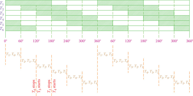
Figure 20.16
Firing scheme for 180° conduction.
If the firing scheme in Figure 20.16 is employed, then the voltages on all the three lines A, B, and C continuously jump from the positive side of the power supply to the negative side (between +VDC and zero) and vice versa. The power supply voltage is always assumed constant. Table 20.1 summarizes the connections for terminals A, B, and C. In this table V and 0 represent the DC voltage and 0, as a result of connection to the positive side or negative side of the power supply, respectively.
A three-phase load is either star connected or delta connected to them, as shown in Figure 20.17. (For simplicity, the freewheeling diodes are not shown.) Figure 20.18 depicts the states of voltages at A, B, and C for the six different intervals of a 360° cycle and the current direction in the three branches of a Y- or Δ-connected load. In columns 3, 4, and 5 a + sign denotes connection to the positive side of the DC power supply and a – sign denotes connection to the negative side. In column 6 showing the currents a 0 indicates that there is no current between the two terminals for that 60° interval.
When the load is star connected, a neutral point is practically defined for the resulting three-phase system. The phase voltage can be found from the voltage difference of the neutral point N and any of the A, B, or C terminals. Figure 20.19 can help understand the voltage at point N with respect to the power supply at each interval of a cycle. The principle of a voltage divider is used for this purpose based on a balanced three-phase resistive load connected to the inverter output.

Figure 20.17
Δ- and star-connected loads to an inverter output.
Table 20.1 Thyristors that are on and Voltages at Terminals A, B and C at 60° Intervals for 180° Conduction
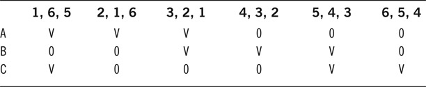
Figure 20.19 also shows the currents in the three lines for a resistive load, for Y and Δ connection. These currents are proportional to the voltages for this load and have the same waveform similar to the voltage variation. For inductive and capacitive loads, current variation is affected by the load reactance and is smoothed out, as was seen for the single-phase inverter.
The line (phase-to-phase) voltages VA − VB, VB − VC, and VC − VA, shown as VA–B, VB–C, and VC–A, respectively, are presented in Figure 20.20. As can be seen, the three alternating currents of square waveform are 120° out of phase with respect to each other, and the voltage varies between plus and minus VDC. This figure also illustrates the line to neutral voltage (phase voltage) variation denoted by VA–N, VB–N, and VC–N. On the basis of the facts depicted in Figures 20.19 and 20.20 the phase voltage fluctuates between plus and minus 2VDC/3, and the neutral line can be connected to the negative side of the power supply.
In a simple three-phase inverter, at each instant the line voltage is the difference between a terminal connected to the positive side and one connected to the negative side; thus, the line voltage is equal to 2× the supply (battery) voltage VDC.
20.4.2 120° Conduction
In the preceding firing scheme each thyristor was on for 180° period and off for 180°. It is possible to use an alternative scheme with 120°conduction instead of 180°. In this case each thyristor conducts for 120° followed by an interval of 240° silence. At each interval of 60°, thus, only two thyristors (from two different legs) conduct. When a thyristor is on for a shorter time, less energy is consumed in it. This scheme is shown in Figure 20.21.

Figure 20.18
Details of voltages and currents for 180° conduction firing scheme in Δ- and Y-connected resistive loads.
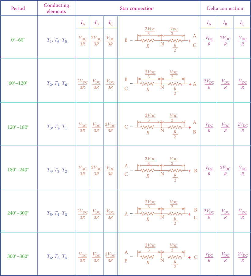
Figure 20.19
Understanding the voltage at the neutral (reference) point in an inverter with 180° firing scheme.
For this firing scheme at each 60° interval of a cycle the two points that are connected to the power supply positive and negative terminals are shown in Table 20.2. Consider a Y-connected load to the resulting three-phase electricity. The neutral point N is at equal voltages for the two connecting terminals at a time. The voltages on each of the A, B, and C terminals vary between +VDC and zero. Thus, a point at the midrange of the power supply can be considered the neutral for the three-phase system. (If this point is available, it can be physically used as the neutral.)
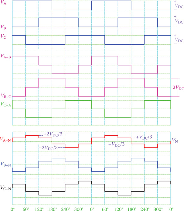
Figure 20.20
Voltage relationships in the generated three-phase waveforms from a six-step inverter with 180° firing.
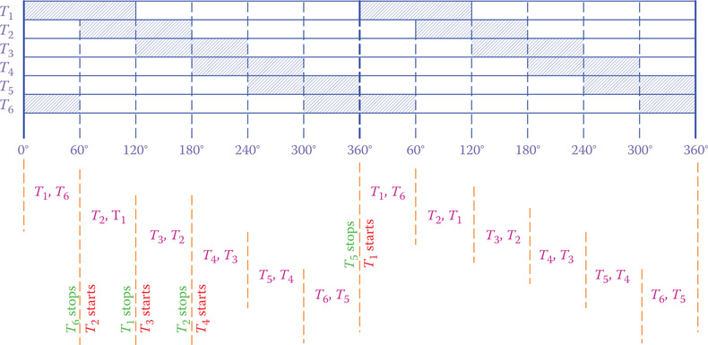
Figure 20.21
A 120° conduction firing scheme.
Table 20.2 Thyristors that are on (two) and Voltages at Terminals A, B and C at 60° Intervals for 120° Conduction

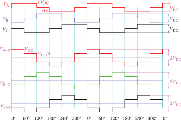
Figure 20.22
Waveform of a six-step inverter with 120° firing scheme.
Figure 20.22 illustrates the variation of phase voltages, based on which the line voltages VA–B, VB–C, and VC–A can be found and are also shown. As depicted in Figures 20.20 and 20.22, in both 180° and 120° conduction the maximum–minimum range for the output waveforms from an inverter is two times the DC supply voltage.
As can be understood from Table 20.2 or Figure 20.21, for this triggering scheme it is not necessary to turn off a thyristor before its counterpart is turned on. This is because the two thyristors to be switched (on or off) at the end of a 60° interval do not belong to the same leg.
Figure 20.23 depicts what happens during one cycle (360°) as far as the voltage and current change in Δ-connected and star-connected loads are concerned. In columns 3, 4, and 5 of this figure, + denotes connection to the positive side of DC power supply, – represents connection to the negative side of the power supply and, NC stands for “not conducting” (see Table 20.2). This is for a pure resistive load. The corresponding currents are shown in Figure 20.24, accordingly.
20.5 Power Converter
You have noticed by now that (compare Figures 20.10 and 20.15 together and Figures 20.11 and 20.21 together) a three-phase rectifier has the same
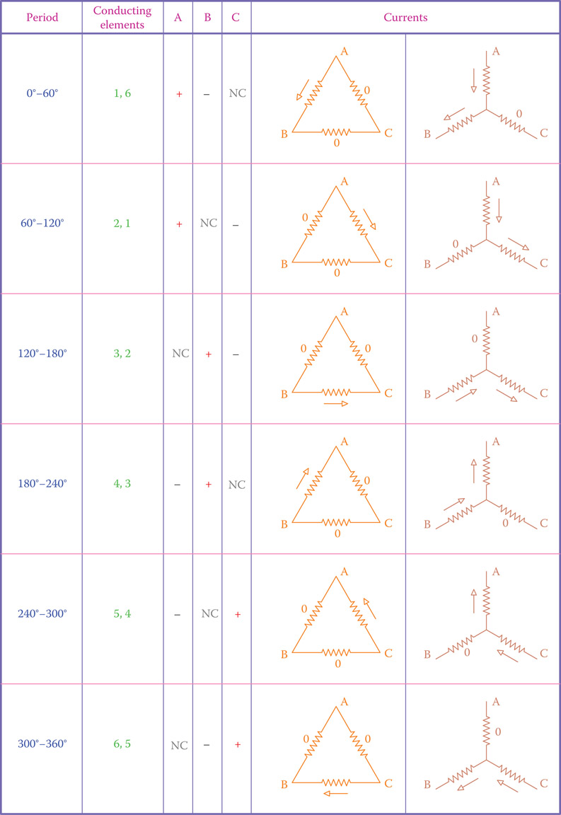
Figure 20.23
Voltages and currents for 120° conduction in Δ- and star-connected loads.

Figure 20.24
Understanding the currents in the three phases for a six-step inverter with 120° firing scheme.
structure and the same elements as a three-phase inverter. For this reason both are referred to as three-phase converters, and because they can be built for carrying medium to large power, they are called power converters.
In fact, Equation 20.2 indicates that in a rectifier if the firing angle α is 90°, then the output has zero voltage. This can be observed from Figure 20.25 that shows how for α = 90° out of the pair of thyristors that must be on at the same time only one is conducting, and, therefore, no voltage can be passed to the output. A firing angle of 0° is also included in Figure 20.25, for comparison. It also implies that if 90° < α < 180°, then the value of DC voltage is negative. Negative DC voltage can be interpreted that if DC power is available in the output, then it can flow in the reverse direction through the switching devices and be converted to AC. This makes it convenient, in practice, because the same device (shown in Figure 20.10 or 20.15) can be used for two different purposes. That is, by changing the triggering times (firing angle) of thyristors the same device (or the same circuit) can be used as a rectifier or as an inverter. If the firing angle is smaller than 90°, the circuit functions as a rectifier, and if the firing angle is greater than 90°, it functions as an inverter.
By changing the firing angle a three-phase converter can behave as a rectifier or can function as an inverter. To act as a rectifier, the firing angle must be smaller than 90°, and to serve as an inverter, the firing angle must be greater than 90°.

Figure 20.25
A firing angle of (a) 0 and (b) 90° for a rectifier. 90° firing angle leads to zero output.
20.6 Pulse Width Modulation
Pulse width modulation (PWM) is frequently used in electronic operations and circuits for both DC and AC electricity. Among its applications in DC is voltage control. Among its AC applications in addition to voltage control is shaping the output of an inverter. As we have seen before, the output of an inverter is not a sine wave. Using PWM allows generation of an AC signal with a better resemblance to a sinusoidal waveform.
Pulse width modulation (PWM): One way of adjusting/controlling the value of a variable by repeated pulses of appropriate width at a proper frequency. These pulses can directly denote a controlled variable, thus their average defines the value of that variable; or they can be part of the control system.
20.6.1 DC Voltage Regulation by Pulse Width Modulation
The principle of pulse width modulation is shown in Figure 20.26 for a simple case of obtaining a smaller desired DC voltage from a DC power supply. In Section 20.3 (see Figure 20.14) we learned that a DC output of a rectifier may have ripples and even blank intervals. Average DC voltage then depends on the variation of the voltage level, taking into account zero values for the blank intervals.

Figure 20.26
Principle of pulse width modulation. (a) Wider pulses lead to higher average compared to (b) with narrower pulses and lower average. (c) Pulse width can be found from position of MN in triangle LPQ.
In Figure 20.26a a repeated series of pulses of constant voltage and constant width (duration), all with the same polarity, are sent across a wire. The width of pulses and the frequency of sending them are important and define the properties of their effects. Pulse width represents its duration and is denoted by a in the figure. Frequency defines the elapsed time between sending the next pulse, which is denoted by b in the figure. Thus, the pulses are sent every b second, and each pulse has a second duration. By this definition, a < b, and its maximum value can be b. If the voltage of each pulse is V volts, then the average voltage in the wire is determined by a, b, and V, i.e.,
| VAv=abV | (20.3) |
For example, if a is half of b and V = 15 V, then the average voltage is 7.5 V. In practice, a and b can be very small, say, a few milliseconds. Suppose that b = 5 msec, a = 2 msec, and V = 15 V. Then the frequency of pulses is 200 (1/0.005) Hz, and the voltage in the line is 6 V. If a is 0, then no pulses are sent and the (average) voltage is 0.
Figure 20.26c shows the relationship in Equation 20.3. Line MN represents a and can assume any position inside the triangle. When it coincides with PQ, a = b and the available voltage is equal to the supply voltage; when it is at point L, a = 0 and the output voltage is zero. Voltage can be represented by the distance of line PQ from point L.
In practice, the width of an electric pulse and its frequency can be controlled by electronic circuits. These pulses from a low-power function generator can trigger high-power devices to turn on and off and generate high-power pulses for the required applications. For instance, the low-power pulses can be applied to the gates of thyristors and control their outputs. Any thyristor to be used for this purpose must be of the type that can be turned on and off, as necessary.
20.6.2 PWM for AC Generation
Both single-phase and three-phase inverters can use pulse width modulation technique for their operation. There are many varieties of employing pulse width modulation for the operation of inverters. The basic principle is the same as was described for DC voltage control. In an inverter, as far as the output voltage is concerned, the thyristors conduct for short periods, thus generating a series of pulses, instead of conducting for 180° or 120° duration (remember the two schemes for inverter functioning). In this way, during any given period of time, thyristors conduct for much shorter intervals but more frequently. For example, in every 20 msec (corresponding to 50 Hz) instead of switching on and then off only once, they turn on and off 40 times or more.
For AC electricity, in addition to the voltage that must be controlled as required, the waveform and frequency need also to be looked after. The average output voltage variation must be as close to a sinusoidal waveform as possible, and the voltage and frequency must be as desired. Note that all the pulses have the same voltage intensity; only their width can vary.
Figure 20.27 shows two possible scenarios for pulses in a single-phase inverter intended for a sine wave output. The difference between them is in the plus and minus polarity change for the pulse train in Figure 20.27a, whereas in Figure 20.27b all pulses have the same polarity. In other words, in Figure 20.27a the neutral point of the resulting AC waveform is defined, whereas in Figure 20.27b it is floating. Note that in both cases the number of pulses per cycle is odd and they are symmetric with respect to the zero crossing point of the intended waveform.
The frequency of the pulses and width of each pulse need to be known for pulse width modulation. Undoubtedly, frequency of sending pulses must be considerably higher than the frequency of the desired output waveform to be generated. Switching action is required for each pulse, and there are energy losses for each switching. Therefore, the number of pulses must be compromised. For a frequency of 60 Hz for the waveform the pulse train can have a frequency of several times like 1000–2000 Hz.
Carrier: A waveform of relatively high frequency in pulse width modulation and other applications (especially in communications) that behaves as a carrier to transfer or treat signals of low-frequency such as voice (in telecommunication) and an electric alternating current waveform (50–60 Hz).
20.6.3 PWM-Controlled Inverter
From the above discussion it can be understood that for pulse width modulation it is essential to define the width of the pulses to be generated. To determine the pulse width at each instant of time for generating a sinusoidal waveform with a desired frequency and voltage a so-called carrier, which is normally a triangular wave, is employed. This carrier is compared to the desired waveform with the required frequency. Then based on this comparison the duration of pulses are determined.

Figure 20.27
Pulse trains for generation of AC waveforms. (a) With positive and negative power supply, (b) with only one power supply.
In practice, all this process can be done offline by a computer. The results are, then, transferred to the actual device. Figure 20.28 can help to understand the modulation process. For better clarity the triangular waveform shown has a much smaller frequency than what happens in practice.
In Figure 20.28a a triangular carrier wave, to be modulated by a reference sine wave, and the modulating wave are plotted together. This reference wave is the desired sinusoidal AC to be generated by the inverter. The points of intersection of the two waves are numbered 1 to 10. As can be observed, for the interval between 1 and 2 the carrier wave is larger (greater magnitude) than the modulating wave, but for the interval 2 to 3 the modulating function has a larger magnitude. The latter is true for the intervals between 4&5, 6&7, and 8&9. Pulses to be generates are all defined by the points of intersection of the two waves, as follows. For those intervals that the carrier is larger than the modulating wave, there is no pulse, and for the intervals that the modulating wave is larger than the carrier, there is a pulse. For each pulse, width is defined by the horizontal spacing (time interval) between the two associated intersection points. On the basis of the scenario shown in Figure 20.28a the corresponding pulses are shown in Figure 20.28b.
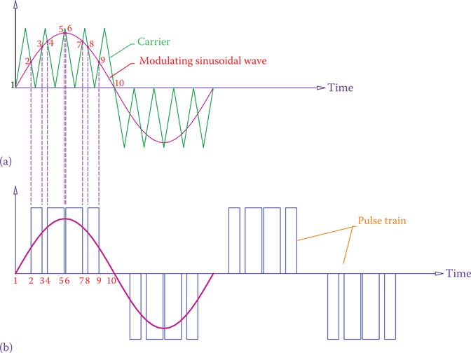
Figure 20.28
Modulating a triangular wave to determine the pulse width for sinusoidal wave generation. (a) Determining the width for pulses. (b) The required pulses.
In PWM, there is no pulse for those intervals when the carrier is larger than the modulating wave. For the intervals when the modulating wave is larger than the carrier, there is a pulse.
The pulses will be used to trigger the thyristors in an inverter. For a single-phase inverter it is easy to see which thyristors must be turned on or off. At each instant, one thyristor from one leg and its counterpart from the other leg must be turned on at the same time (see Figure 20.1). If the scheme in Figure 20.27b is used (no polarity change for pulses), it is possible to reduce the number of switching action. For this scheme it is possible to keep one of the thyristors on for the whole half cycle and only send pulses to its counterpart. This is shown in Figure 20.29. This method is not practicable for the scheme with polarity change pulses (Figure 20.27a).
Note that to generate the pulse train in Figure 20.29 (without polarity change) the same principle is used and the pulse widths are determined based on comparison of the modulating wave and a carrier wave without polarity. The carrier wave has a larger amplitude than the reference waveform (compare Figures 20.28a and 20.29); otherwise, not sufficient intersections can be found. For thyristor numbering, see Figure 20.1.
In practice, the two waves (the carrier and the modulator) can be compared (by a comparator circuit) to determine which one has a larger magnitude. If digital systems (or a digital computer) are used, then it is possible to put the results of the comparison in memory and send the pulses using a memory look-up table. Among other alternative ways to determine the pulse widths is employing mathematical functions that result in a waveform that better resembles a sine wave. Again, the results can be read from memory-stored data.

Figure 20.29
Continuous pulses without polarity and with less switching (refer to Figure 20.1).
Note that in using pulse width modulation both the amplitude ratio and the frequency ratio of the carrier wave to the reference (desired) wave affect the number and width of the pulses. These two parameters are called frequency modulation ratio and amplitude modulation ratio and are denoted by mf and ma, as
Frequency modulation ratio: Ratio of the frequency of the carrier signal to that of the reference signal in pulse width modulation, used in power converters, a number larger than 1 and represented by mf.
Amplitude modulation ratio: Ratio of the amplitude of the reference signal to that of the carrier signal in pulse width modulation, used in power converters.
| mf=fcfr=carrier frequencyreference frequency=frequency modulation ratio | (20.4) |
| ma=VrVc=reference voltagecarrier voltage=amplitude modulation ratio | (20.5) |
To see the effect of changing amplitude modulation ratio, see Figure 20.30 and compare the pulses in the two cases shown (focus on width of the pulses). For the effect of changing frequency modulation ratio, compare Figures 20.29 and 20.30. Count the numbers of pulses and the frequency of the carrier for one cycle of the sinusoidal waveform (10 in Figure 20.29 and 9 in Figure 20.30. Also, observe the symmetry). The value of mf is always greater than 1; it is an odd multiplier of 3 for technical reasons, and its range of values can be between 21 and 35, for instance. The value of ma is normally less than 1. If it has a magnitude larger than 1, it represents overmodulation, which causes distortion in the resulting signal generated from the pulses.
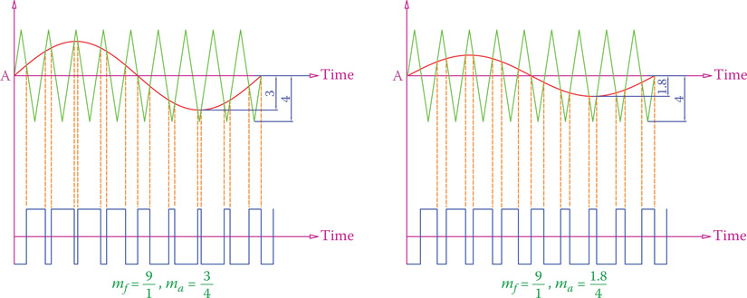
Figure 20.30
Effect of amplitude modulation ratio.
Overmodulation: Having a value larger than 1 for amplitude modulation ratio in pulse width modulation controlled inverters. This happens when the amplitude of the modulating signal is greater than that of the carrier wave.
20.6.4 Pulse Width Modulation for Three-Phase Inverter
The PWM scheme depicted in Figures 20.27 and 20.28 for a single-phase inverter can be extended to three-phase systems. Because there is a 120° phase difference between the three phases, the same pattern for one phase repeats, only with a shift in time. In other words, the same scheme for pulse widths and timing can be used for each individual phase; only they must have a timing shift corresponding to 120° with respect to each other. Figure 20.31 shows the case.
The three pulse trains shown in Figure 20.31 can be used to trigger the gates of the six thyristors in a three-phase inverter. For three-phase system it is not possible to keep any of the thyristors turned on (like the case for a single-phase inverter); thus, a lot of switching is necessary. At each instant, one thyristor of each leg is on and the other is off. At each edge of every pulse (i.e., for both rising edge and falling edge) one thyristor in a leg of the inverter is turned off and the other is turned on, as shown for phase C in Figure 20.32. The thyristor numbers correspond to the arrangement in Figure 20.15.
For a three-phase converter it is not possible to keep any of the thyristors on for a period longer than the associated pulse width.

Figure 20.31
A, Pulse trains for three phases using PWM; B, time intersection of pulses for phase A and their counterpart pulses for B and C.

Figure 20.32
Triggering thyristors for three-phase system inverters using PWM.
For a pulse width modulation inverter to work properly the frequency of the carrier wave must be sufficiently larger than the modulating wave frequency; that is, the modulation frequency ratio needs to be greater than 20. Also, overmodulation is not desirable; thus, the amplitude modulation ratio must be smaller than 1.
20.7 Application in Motor Drives
From the knowledge gained in Chapter 11 on AC electric motors and in this chapter about power converters you observe that
- The speed of an AC motor depends on the line frequency.
- A converter can change DC to AC with a desired frequency.
- A converter can also change AC to DC.
Putting together all these facts and the available technology has led to the generation of a family of devices that can be used today for driving motors. Noting that at the industry level the main supply of electricity is in the form of three-phase AC, we can see that
- DC electricity can be obtained from AC.
- Single-phase or three-phase electricity with a desired frequency can be obtained from DC.
Also,
- 3. The frequency of a converter output can be controlled.
- 4. AC-to-DC and DC-to-AC converters can be put back to back. In such a case, a frequency converter is devised that can provide a variable frequency – variable voltage AC from a fixed frequency AC supply.
As a result, by employing appropriate converters nowadays, (1) DC motors can be run from AC sources and (2) an AC motor speed can be varied as desired. This includes the starting of motors in such a way that they start smoothly without putting too much stress on the machine or on a circuit.
For alternating current machines these devices are called variable speed drives (VSD), or variable frequency drive (VFD), mentioned in Chapter 9. They appear in various forms and at various powers with a variety of options, such as single-phase output from three-phase input, or vice versa in addition to DC output for DC machines.
20.8 Chapter Summary
- An inverter is used to generate AC from DC electricity. An inverter is the opposite of a rectifier.
- An inverter works based on repeatedly altering the direction of current in its load.
- Inverters use switchable diodes or transistors.
- Both single-phase and three-phase inverters are possible.
- Simpler inverters generate square wave. Inverters with an output of stepping waveform have better resemblance to sine wave.
- Single-phase inverters need at least four switching elements; three-phase inverters need six.
- Firing angle is the delay in turning a thyristor or a transistor on, expressed in terms of degrees (referring to a cycle of an AC waveform; that is, 360°). Firing angle is with respect to zero crossing (0° of the AC waveform).
- If rectifiers are made with switchable diodes, their output voltage can be controlled.
- In a rectifier, firing angle can be altered between 0 and 90°.
- In inverters, each switching device has a freewheel diode in parallel with it, but with the opposite polarity (antiparallel). The freewheel diode is for safety and protection of a device.
- In switching devices, there is always some power loss associated with switching.
- Maximum output voltage of an inverter depends on the DC power supply.
- A converter can refer to a rectifier or an inverter because both have the same structure.
- In a three-phase converter if the firing angle is smaller than 90°, the circuit functions as a rectifier, and if the firing angle is greater than 90°, it functions as an inverter.
- Pulse width modulation (PWM) implies defining a pulse train with specified widths of pulses (in terms of time) and frequency to be used for a desired application, such as voltage regulation.
- PWM can be used in single-phase and three-phase inverters and in DC electricity.
- For PWM a carrier wave with much higher frequency is modulated by a reference wave to determine the rate and width of the pulses in a pulse train.
- Both amplitude and frequency of the carrier wave are involved in defining the pulse train.
- The higher the frequency of the pulse train, the closer is the form of an inverter output to the reference (desired) wave but also the more are the switching actions and the energy loss due to switching.
- In inverters the amplitude modulation ratio is the ratio of reference wave voltage to that of the carrier wave. Also, the frequency modulation ratio is the ratio of carrier wave frequency to that of the reference wave.
- If the amplitude modulation ratio is larger than 1, overmodulation occurs, which is undesirable.
Review Questions
- What is an inverter for?
- What is the functioning principle of an inverter?
- What are the main components of an inverter?
- Can an inverter work with ordinary diodes? Why or why not?
- Is the output of an inverter a sinusoidal AC wave? Why or why not?
- If for single-phase inverters four thyristors are required, how many does one need for a three-phase inverter?
- How can the quality of the output waveform of an inverter be improved to better resemble a sine wave?
- Can the output voltage of an inverter be controlled?
- How can the output voltage of an inverter be changed?
- What is the firing angle in a rectifier?
- What is the firing angle in a diode rectifier?
- If a single-phase rectifier is used for a 120 V, 50 Hz line, what is the DC voltage?
- If the same rectifier as in the previous question is used on a 60 Hz line (same voltage), what is the DC voltage?
- What is a freewheel diode for, and where is it used?
- With a 12 V battery, what is the peak-to peak of the AC electricity obtained from a single-phase inverter?
- What is the difference between 180°- and 120°- conducting three-phase inverters?
- How many thyristors are necessary for a three-phase rectifier?
- What does PWM stand for?
- Name two applications of PWM.
- Can one use a three-phase rectifier as a three-phase inverter? Why or why not?
- How can frequency of the AC from an inverter be changed?
- How can output voltage of an inverter be increased?
- Explain what a power converter is.
- What is frequency modulation ratio?
Problems
- A three-phase diode-based rectifier is used on a line with 120 V line-to-neutral voltage. What is the DC voltage, ignoring the losses?
- If the firing angle in a three-phase rectifier used on 380 V line is 25°, what is the DC voltage?
- What is the effective voltage of the output of a converter with sufficiently accurate sine waveform if the DC input is 11,050 V DC?