
Boolean algebra
4.1 Introduction
Boolean algebra can be thought of as the study of the set {0, 1} with the operations + (or),. (and), and − (not). It is particularly important because of its use in design of logic circuits. Usually, a high voltage represents TRUE (or 1), and a low voltage represents FALSE (or 0). The operation of OR (+) is then performed on two voltage inputs, using an OR gate, AND(.) using an AND gate and NOT is performed using a NOT gate. This very simple algebra is very powerful as it forms the basis of computer hardware.
You will probably have noticed that the operations of Λ (AND), ∨ (OR), and ¬ (NOT) used in Chapter 3 for propositions are very similar to the operations ∩ (AND), ∪ OR, and ′ (NOT) (complement) used for sets. This connection is not surprising as membership of a set, A, could be defined using a statements like ‘3 is a member of A’ which is either TRUE or FALSE. In simplifying logic circuits, use is made of the different interpretations that can be put upon the operations and variables. We can use truth tables, borrowed from the theory of propositions, as given in Chapter 3, or we can use Venn diagrams, borrowed from set theory, as given in Chapter 1.
The first thing we shall examine in this chapter is what do we mean by an algebra and why are we able to skip between these various interpretations. Then we look at implementing and minimizing logic circuits.
4.2 Algebra
Before we look at Boolean algebra, we will have a look at some ideas about algebra:
(b) What is an operation?
(c) What do we mean by properties (or laws or axioms) of an algebra?
An algebra is a set with operations defined on it. In Chapter 1 of the Background Mathematics Notes, available on the companion website for this book, we looked at the algebra of real numbers and defined an operation is a way of combining two numbers to give a single number. We could therefore define an operation as a way of combining two elements of the set to result in another element of the set.
Example 4.1
The set of real numbers, ![]() , has the operations + and., for example,
, has the operations + and., for example,
![]()
and we could combine any two numbers in this way and we would always get another real number.
Example 4.2
Consider the set of sets in some universal se ε, for example,
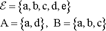
then
![]()
The operations of ∩and ∪ also result in another set contained in ![]() .
.
In both of these examples, the operations are binary operations because they use two inputs to give one output.
There is another sort of operation which is important, called a unary operation, because it only has one input to give one output. Consider Example 4.2: A′ = {b, c, e} gives the complement of A. This is a unary operation as only one input, A, was needed to define the output A'.
If we can find a rule which is always true for an algebra then that is called a property, (law or axiom) of that algebra. For example, (3 + 5) + 4 = 3 + (5 + 4) is an application of the associative law of addition which can be expressed in general in the following way for the set of real numbers:
![]()
If we can list all the properties of a particular algebra then we can give that algebra a name. For instance, the real numbers with the operations of + and. form a field.
4.3 Boolean algebras
Sets as a Boolean algebra
The sets contained in some universal set display a number of properties which can be shown using Venn diagrams.
Example 4.3
Show, using Venn diagrams, that, for any 3 sets A, B, C in some universal set ![]() ,
,
![]()
Solution This can be shown to be true by drawing a Venn diagram of the left-hand side of the expression and another of the right-hand side of the expression. Operations are performed in the order indicated by the brackets and the result of each operation is given a different shading. This is done in Figure 4.1(a) and (b). The region shaded in Figure 4.1(a) representing A ∩ (B ∪ C) is the same as that representing (A ∩ B) ∪ (A ∩ C) in Figure 4.1(b), hence, showing that A ∩ (B ∪ C) = (A ∩ B) ∪ (A ∩C).

In the same way, other properties can be shown to be true. A full list of the properties gives:
For every A, B, C ⊆ ![]()
| (B1) A ∪ A = A | A ∩ A = A | Idempotent |
| (B2) A ∪ (B ∪ C) = (A ∪ B) ∪ C | A ∩ (B ∩ C) = (A ∩ B) ∩ C | Associative |
| (B3) A ∪ B = B ∪ A | A ∩ B = B ∩ A | Commutative |
| (B4) A ∪ (A ∩ B) = A | A ∩ (A ∪ B) = A | Absorption |
| (B5) A ∪ (B ∩ C) = (A ∪ B) ∩ (A ∪ C) | A ∩ (B ∪ C) = (A ∩ B) ∪ (A ∩ C) | Distributive laws |
| (B6) A ∪ | A ∩ ∅ = ∅ | Bound laws |
| (B7) A ∪ ∅ = A | A ∩ | Identity law |
| (B8) A ∪ A' = ɛ | A ∩ A' = ∅ | Complement laws |
| (B9) ∅' = | 0 and 1 laws | |
| (B10) (A ∪ B)' = A' ∩ B' | (A ∩ B)' = A' ∪ B' | De Morgan's laws |
Notice that all the laws come in pairs (called duals). A dual of a rule is given by replacing ∪ by ∩and ∅ by ![]() and vice versa.
and vice versa.
Propositions
We looked at propositions in Chapter 3. Propositions can either be given a value of TRUE (T) or FALSE (F). Examples of propositions are 3 = 5 which is false and 2 < 3 which is true. The logical operators of AND, OR, and NOT are defined using truth tables, which we repeats in Table 4.1.

Properties of propositions and their operations can be shown using truth tables.
Example 4.4
Show, using truth tables, that for any propositions p, q, r
![]()
Solution The truth tables are given in Table 4.2. Note that there are eight lines in the truth table in order to represent all the possible states (T, F) for the three variables p, q, and r. As each can be either TRUE or FALSE, in total there are 23 = 8 possibilities. To find (p ∧ q) ∧ r, p ∧ q is performed first and the result of that is ANDed with r. To find p ∧ (q ∧ r) then q ∧ r is performed first and p is ANDed with the result. As the resulting columns are equal we can conclude that
![]()
Table 4.2
A truth table to show (p ![]() q)
q) ![]() r ⇔ p
r ⇔ p ![]() (q
(q ![]() r). The fifth column gives the truth values of (p
r). The fifth column gives the truth values of (p ![]() q)
q) ![]() r and the seventh column gives the truth value of p
r and the seventh column gives the truth value of p ![]() (q
(q ![]() r). As the two columns are the same we can conclude that (p
r). As the two columns are the same we can conclude that (p ![]() q)
q) ![]() r ⇔ p
r ⇔ p ![]() (q
(q ![]() r)
r)
| p | q | r | p | (p | q | p |
| T | T | T | T | T | T | T |
| T | T | F | T | F | F | F |
| T | F | T | F | F | F | F |
| T | F | F | F | F | F | F |
| F | T | T | F | F | T | F |
| F | T | F | F | F | F | F |
| F | F | T | F | F | F | F |
| F | F | F | F | F | F | F |

Example 4.5
Show that for any two propositions p, q:
![]()
Solution The truth table is given in Table 4.3.
Table 4.3
A truth table to show ¬(p ![]() q) ⇔ (¬p) ∨ (¬q). The fourth column gives the truth values of ¬(p ∨ q) and the seventh column gives the truth value of (¬p)
q) ⇔ (¬p) ∨ (¬q). The fourth column gives the truth values of ¬(p ∨ q) and the seventh column gives the truth value of (¬p) ![]() (¬q). As the two columns are the same we can conclude that ¬(p
(¬q). As the two columns are the same we can conclude that ¬(p ![]() q) ⇔ (¬p) ∨ (¬q)
q) ⇔ (¬p) ∨ (¬q)
| p | q | p | ¬(p | ¬p | ¬q | ¬p ∨ ¬q |
| T | T | T | F | F | F | F |
| T | F | F | T | F | T | T |
| F | T | F | T | T | F | T |
| F | F | F | T | T | T | T |

It turns out that all the properties we listed for sets are also true for propositions. We list them again, for any three propositions p, q, r
| (B1) p ∨ p ⇔ p | p | Idempotent |
| (B2) p ∨ (q ∨ r) ⇔ (p ∨ q) ∨ r | p | Associative |
| (B3) p | p | Commutative |
| (B4) p ∨ (p | p | Absorption |
| (B5) p ∨ (q | p | Distributive laws |
| (B6) p ∨ T ⇔ T | p | Bound laws |
| (B7) p ∨ F ⇔ p | p | Identity laws |
| (B8) p ∨ ¬p ⇔ T | p | Complement laws |
| (B9) ¬F ⇔ T | ¬T ⇔ F | 0 and 1 laws |
| (B10) ¬(p ∨ q) ⇔ ¬p | ¬(p | De Morgan's laws |
Notice again that all the laws are duals of each other. A dual of a rule is given by replacing ∨ by ∧ and F by T, and vice versa.
The Boolean set {0, 1}
The simplest Boolean algebra is that defined on the set {0, 1}. The operations on this set are AND (.), OR (+), and NOT(−). The operations can be defined using truth tables as in Table 4.1, shown again in Table 4.4. This time notice that the first two are usually ordered in order to mimic binary counting, starting with 0 0, then 0 1, then 1 0, then 1 1. This is merely a convention and the rows may be ordered any way you like. a and b are two variables which may take the values 0 or 1.
Table 4.4
The operations of AND (.), OR (+) and NOT (−) defined for any variables a, b taken from the Boolean set {0,1}
| a | b | a.b | a | b | a + b | a | ā |
| 0 | 0 | 0 | 0 | 0 | 0 | 0 | 1 |
| 0 | 1 | 0 | 0 | 1 | 1 | 1 | 0 |
| 1 | 0 | 0 | 1 | 0 | 1 | ||
| 1 | 1 | 1 | 1 | 1 | 1 |

This now looks far more like arithmetic. However, beware because although the operation AND behaves like multiplication, 0.0 = 0, 0.1 = 0,1.0 = 0 and 1.1 = 1 as in ‘ordinary′ arithmetic, the operation OR behaves differently as 1 + 1 = 1.
All the laws as given for sets and for propositions hold again and they can be listed as follows:
For any three variables a, b, c ∈ {0, 1}
| (B1) a + a = a | a.a = a | Idempotent |
| (B2) a + (b + c) = (a + b) + c | a.(b.c) = (a.b).c | Associative |
| (B3) a + b = b + a | a + b = b + a | Commutative |
| (B4) a + (a.b) = a | a.(a + b) = a | Absorption |
| (B5) a + (b.c) = (a + b).(a + c) | a.(b + c) = (a.b) + (a.c) | Distributive laws |
| (B6) a + 1 = 1 | a.0 = 0 | Bound laws |
| (B7) a.1 = a | a + 0 = a | Identity laws |
| (B8) a + ā = 1 | a.ā = 0 | Complement laws |
| (B9) | ī = 0 | 0 and 1 laws |
| (B10) | De Morgan's laws |
We often leave out the‘.’ so that ‘ab’ means ‘a.b’. We also adopt the convention that. takes priority over + hence miss out some of the brackets.
Example 4.6
Evaluate the following where +,., and – are Boolean operators.
(b) ![]()
(c) ![]()
Solution
(a) We use the convention that. is performed first:
![]()
(b) ![]()
(c) ![]()
The algebraic laws can be used to simplify a Boolean expression.
Example 4.7
Simplify
![]()
Solution

Although it is possible to simplify in this way, it can be quite difficult to spot the best way to perform the simplification; hence, there are special techniques used in the design of digital circuits which are more efficient.
4.4 Digital circuits
Switching circuits form the basis of computer hardware. Usually, a high voltage represents TRUE (or 1) while a low voltage represents a FALSE (or 0). Digital circuits can be represented using letters for each input.
There are three basic gates which combine inputs and represent the operators NOT(−), AND (.), and OR (+). These are shown in Figure 4.2.

Other gates
Other common gates used in the design of digital circuits are the NAND gate, ![]() that is, not(ab), the NOR gate,
that is, not(ab), the NOR gate, ![]() that is, not(a + b) and the EXOR gate a⊕b, (exclusive or) a⊕b =
that is, not(a + b) and the EXOR gate a⊕b, (exclusive or) a⊕b = ![]() These gates are shown in Figure 4.3.
These gates are shown in Figure 4.3.

 , NOR
, NOR  , and EXOR (a ⊕ b).
Implementing a logic circuit
First, we need to simplify the expression. Each letter represents an input that can be on or off (lor 0). The operations between inputs are represented by the gates. The output from the circuit represents the entire Boolean expression.
Example 4.8
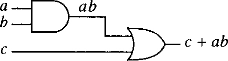
Implement ![]()
Solution We can use absorption to write this as ![]() and this can be implemented as in Figure 4.4 using AND, OR, and NOT gates. Alternatively, we can use the distributive and De Morgan's laws to write the expression as:
and this can be implemented as in Figure 4.4 using AND, OR, and NOT gates. Alternatively, we can use the distributive and De Morgan's laws to write the expression as:
![]()

 (b) An alternative implementation using
which can be implemented using an AND and a NAND gate.
Minimization and Karnaugh maps
It is clear that there are numbers of possible implementations of the same logic circuit. However, in order to use less components in building the circuit it is important to be able to minimize the Boolean expression. There are several methods for doing this. A popular method is using a Karnaugh map. Before using a Karnaugh map, the Boolean expression must be written in the form of a ‘sum of products,. To do this, we may either use some of the algebraic rules or it may be simpler to produce a truth table and then copy the Os and 1s into the Karnaugh map. Example 4.9 is initially in the sum of product form and Example 4.10 uses a truth table to find the Karnaugh map.
Example 4.9
Minimize the following using a Karnaugh map:
![]()
and draw the implementation of the resulting expression as a logic circuit.
Solution Draw a Karnaugh map as in Figure 4.5(a). If there are two variables in the expression then there are 22 = 4 squares in the Karnaugh map. Figure 4.5(b) shows a Karnaugh map with the squares labelled term by term. Figure 4.5(c) shows that the map is like a Venn diagram of the sets a and b. In Figure 4.5(a) we put a 0 or 1 in the square depending on whether that term is present in our expression. Adjacent 1s indicate that we can simplify the expression. Figure 4.6 indicates how we go about the minimization. We draw a line around any two adjacent 1s and write down the term representing that section of the map. We are able to encircle the second row, representing a, and the second column, representing b. As all the 1s have now been included we know that a + b is a minimization of the expression. Notice that it does not matter if one of the squares with a 1 in it has been included twice but we must not leave any out. The implementation of a + b is drawn in Figure 4.7.
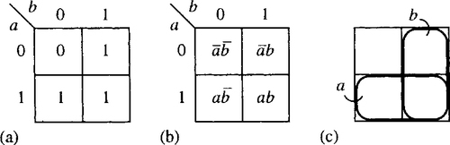
 (b) A two-variable Karnaugh map with all the boxes labelled. (c) A Karnaugh map is like a Venn diagram. The second row represents the set a and the second column represents the set b.
 .
.
Example 4.10
Minimize ![]() and draw the implementation of the resulting expression as a logic circuit.
and draw the implementation of the resulting expression as a logic circuit.
Solution First, we need to find the expression as a sum of products. This can be done by finding the truth table and then copying the result into the Karnaugh map. The truth table is found in Table 4.5. Notice that we calculate various parts of the expression and build up to the final expression. With practice, the expression can be calculated directly for instance when a = 0, b = 0, and c = 0 then ![]()
![]()
Table 4.5
A truth table to find ![]()
| a | b | c | ab | ||||||
| 0 | 0 | 0 | 0 | 1 | 1 | 0 | 1 | 0 | 0 |
| 0 | 0 | 1 | 0 | 0 | 1 | 0 | 1 | 1 | 1 |
| 0 | 1 | 0 | 0 | 1 | 1 | 0 | 1 | 0 | 0 |
| 0 | 1 | 1 | 0 | 0 | 1 | 0 | 1 | 1 | 1 |
| 1 | 0 | 0 | 0 | 1 | 1 | 0 | 1 | 0 | 0 |
| 1 | 0 | 1 | 0 | 0 | 1 | 0 | 1 | 1 | 1 |
| 1 | 1 | 0 | 1 | 1 | 0 | 1 | 1 | 0 | 1 |
| 1 | 1 | 1 | 1 | 0 | 0 | 0 | 1 | 1 | 1 |

Draw a Karnaugh map as in Figure 4.8(a) and copy in the expression values as found in Table 4.5. There are three variables in the expression, therefore, there are 23 = 8 squares in the Karnaugh map.
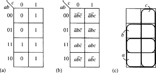
 . (b) A three-variable Karnaugh map with all the boxes labelled. (c) A Karnaugh map is like a Venn diagram. The third and fourth rows represent the set a and the second and third rows represent the set b. c is represented by the second column.
Figure 4.8(b) shows a Karnaugh map with the squares labelled term by term. Figure 4.8(c) shows the Venn diagram equivalence with sets a, b, and c. In Figure 4.8(a) we put a 0 or 1 in the square depending on whether that term is present, as given in the truth table in Table 4.5.
Adjacent l s indicate that we can simplify the expression. Figure 4.9 indicates how we go about the minimization. We draw a line around any four adjacent l s and write down the term representing that section of the map. The second column represents c and has been encircled. Then we look for any two adjacent l s. We are able to encircle the third row, representing ab As all the l s have now been included we know that c + ab is a minimization of the expression. An implementation of c + ab is drawn in Figure 4.10.

Example 4.11
Minimize ![]() using a Karnaugh map and draw the implementation of the resulting expression as a logic circuit.
using a Karnaugh map and draw the implementation of the resulting expression as a logic circuit.
Solution Draw a Karnaugh map as in Figure 4.11(a). There are four variables in the expression therefore there are 24 = 16 squares in the Karnaugh map. Figure 4.11 (b) shows a Karnaugh map with the squares labelled term by term. Figure 4.11 (c) shows the Venn diagram equivalence with sets a, b, c, and d. In Figure 4.11(a), we put a 0 or 1 in the square depending on whether that term is present in our expression. However, the term ![]() involves only three out of the four variables. In this case, it must occupy two squares. As d could be either 0 or 1 for
involves only three out of the four variables. In this case, it must occupy two squares. As d could be either 0 or 1 for ![]() to be true, we fill in the squares for
to be true, we fill in the squares for ![]() and
and ![]() . The number of squares to be filled with a 1 to represent a certain product is 2mwhere m is the number of missing variables in the expression. In this case,
. The number of squares to be filled with a 1 to represent a certain product is 2mwhere m is the number of missing variables in the expression. In this case, ![]() has no d term in it so the number of squares representing it is 21.
has no d term in it so the number of squares representing it is 21.

 . (b) A four-variable Karnaugh map with all the squares labelled. (c) A Karnaugh map is like a Venn diagram. The third and fourth rows represent the set a and the second and third rows represent the set b. c is represented by the third and fourth columns and d by the second and third columns.
Adjacent l s indicate that we can simplify the expression. Figure 4.12 indicates how we go about the minimisation. We draw a line around any eight adjacent ln s of which there are none. Next we look for any four adjacent 1 s and write down the term representing that section of the map. The third row represents ab and has been encircled. The middle four squares represent bd and have been encircled. Then we look for any two adjacent l s. The bottom two squares of the second column represent ![]() . As all the l s have now been included we know that
. As all the l s have now been included we know that ![]() is a minimization of the expression. This is implemented in Figure 4.13.
is a minimization of the expression. This is implemented in Figure 4.13.

 .
.
 .
.Example 4.12
To display the digits 0–9, a seven-segment light emitting diode (LED) display may be used as shown in Figure 4.14. The various states may be represented using a four-variable digital circuit. The logic control signals for the lamp drivers are given by the truth table given in Table 4.6. The X indicates a ‘don't care′ condition in the truth table. The column for the segment labelled p can be copied into a Karnaugh map as given in Figure 4.15. Wherever a 1 appears in the truth table representation for p there is a 1 copied to the Karnaugh map. Similarly, the Os and the ‘don't care′ crosses are copied. Minimize the Boolean expression for p using the Karnaugh map.

Table 4.6
A truth table giving the logic control signals for the lamp drivers for the LED segments pictured in Figure 4.14
| Digit displayed | Circuit inputs | Segments | |||||||||
| a | b | c | d | p | q | r | s | t | u | v | |
| 0 | 0 | 0 | 0 | 0 | 1 | 1 | 1 | 1 | 1 | 1 | 0 |
| 1 | 0 | 0 | 0 | 1 | 0 | 1 | 1 | 0 | 0 | 0 | 0 |
| 2 | 0 | 0 | 1 | 0 | 1 | 1 | 0 | 1 | 1 | 0 | 1 |
| 3 | 0 | 0 | 1 | 1 | 1 | 1 | 1 | 1 | 0 | 0 | 1 |
| 4 | 0 | 1 | 0 | 0 | 0 | 1 | 1 | 0 | 0 | 1 | 1 |
| 5 | 0 | 1 | 0 | 1 | 1 | 0 | 1 | 1 | 0 | 1 | 1 |
| 6 | 0 | 1 | 1 | 0 | 0 | 0 | 1 | 1 | 1 | 1 | 1 |
| 7 | 0 | 1 | 1 | 1 | 1 | 1 | 1 | 0 | 0 | 0 | 0 |
| 8 | 1 | 0 | 0 | 0 | 1 | 1 | 1 | 1 | 1 | 1 | 1 |
| 9 | 1 | 0 | 0 | 1 | 1 | 1 | 1 | 1 | 0 | 1 | 1 |
| − | 1 | 0 | 1 | 0 | X | X | X | X | X | X | X |
| − | 1 | 0 | 1 | 1 | X | X | X | X | X | X | X |
| − | 1 | 1 | 0 | 0 | X | X | X | X | X | X | X |
| − | 1 | 1 | 0 | 1 | X | X | X | X | X | X | X |
| − | 1 | 1 | 1 | 0 | X | X | X | X | X | X | X |
| − | 1 | 1 | 1 | 1 | X | X | X | X | X | X | X |


Solution The minimization is represented in Figure 4.15(b). We first look for any eight adjacent squares with a 1 or a X in them. The bottom two rows are encircled giving the term a. Now we look for groups of four. The central four squares represent bd and the third column represents cd. Finally, we can count the four corner squares as adjacent. This is because two squares may be considered as adjacent if they are located symmetrically with respect to any of the lines which divide the Karnaugh map into equal halves, quarters, or eighths. This means that squares that could be curled round to meet each other, as if the Karnaugh map where drawn on a cylinder, are considered adjacent and also the four corner squares. Here, the four corner squares represent the term ![]() . Hence, the minimization for p gives
. Hence, the minimization for p gives
![]()
4.5 Summary
(1) An algebra is a set with operations defined on it. A binary operation as a way of combining two elements of the set to result in another element of the set. A unary operation has only one input element producing one output.
(2) A Boolean algebra has the operations of AND, OR, and NOT defined on it and obeys the set of laws given in Section 4.3 as (B 1)–(B 10). Examples of a Boolean algebra are: the set of sets in some universal set ![]() , with the operations of ∩, ∪ and′; the set of propositions with the operations of ∧, ∨, and ¬; the set {0, 1} with the operations‘.′ +, and −.
, with the operations of ∩, ∪ and′; the set of propositions with the operations of ∧, ∨, and ¬; the set {0, 1} with the operations‘.′ +, and −.
(3) Logic circuits can be represented as Boolean expressions. Usually, a high voltage is represented by 1 or TRUE and a low voltage by 0 or FALSE. There are three basic gates to represent the operators AND (.), OR (+), and NOT (–).
(4) A Boolean expression may be minimized by first expressing it as a sum of products and then using a Karnaugh map to combine terms.
4.6 Exercises
4.1 Show the following properties of sets using Venn diagrams:
(b) ![]()
4.2 p = ‘It rained yesterday′
q = ‘I used an umbrella yesterday′
(a) Construct English sentences to express, (∧⇔‘and, ∨⇔‘or′ ¬⇔‘not′)
(ii) p ∨ q
(iii) ¬p ∨ q
(iv) p ∧¬q
(v) ¬(p ∧ q)
(vi) ¬p ∨¬q.
(b) Given that p is true and q is false, what is the truth value of each part of section (a)?
4.3 Showthe following properties of propositions using truth tables
(b) ![]()
4.4 Using Venn diagrams or truth tables find simpler expressions for the following:
(b) ![]()
(c) a + abc
(a) Draw implementations of the following as logic circuits:
(ii) a + bc
(iii) ![]()
(iv) ![]()
(b) If a = 1, b = 0 and c = 1, what is the value of each of the expressions in section (a)?
4.6 Minimize the following expressions and draw their logic circuits:
(b) ![]()
(c) ![]()
4.7 Obtain a Boolean expression for the logic networks shown in Figure 4.16.

4.8 Consider the LED segment labelled r in Figure 4.14 given in the text. Follow the method given in
Example 4.12
to find a minimized expression for r and draw its logic network.