![18.6 DESIGN 1: DESIGN SPACE EXPLORATION WHEN s1 = [1 −1]](https://imgdetail.ebookreading.net/cover/cover/software_development/EB9780470934630.jpg)
18.6 DESIGN 1: DESIGN SPACE EXPLORATION WHEN s1 = [1 −1]
Figure 18.2 shows the DAG for the polynomial division algorithm based on our timing function choice s1. The equitemporal planes are the diagonal lines shown as gray lines on the right of the diagram. The associated time index values are shown at the right of the diagram. We note from the figure that the signals corresponding to the coefficients of B and the estimated q output are all pipelined, as indicated by the arrows connecting the nodes. However, the estimated partial results for Q and R are broadcast, as indicated by the diagonal lines without arrows. There are three simple projection vectors such that all of them satisfy Eq. 18.21 for the scheduling function in Eq. 18.17. The three projection vectors will produce three designs:
(18.22)
![]()
(18.23)
![]()
(18.24)
![]()
Figure 18.2 Directed acyclic graph (DAG) for polynomial division algorithm when s1 = [1 −1], n = 9, and m = 5.

The corresponding projection matrices are
(18.25)
![]()
(18.26)
![]()
(18.27)
![]()
Our design space now allows for three configurations for each projection vector for the chosen timing function. As it turns out, the choice of d1b or d1c would produce n nodes or tasks but only m of them are active at any time step. Through proper relabeling of the tasks, we would obtain the design corresponding to d1a. Therefore, we consider only the case when s1 and d1a. There will be m tasks that are all active at each time step. The design will result in the well-known Fibonacci (Type 1) LFSR. A point in the DAG given by the coordinates p = [i j]t will be mapped by the projection matrix P1a into the point ![]() = P1ap. The
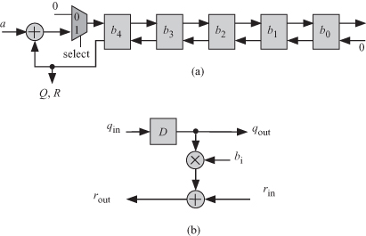
= P1ap. The ![]() corresponding to design 1 is shown in Fig. 18.3. There will be m tasks where input coefficients of A are fed from the right and the partial remainders are pipelined among the processors. Coefficient bj of divisor polynomial B is stored in task Tj. The task processing details are shown in Fig. 18.3b for hardware systolic implementation where D denotes a 1-bit register to store the partial output. The input to the LFSR is obtained from a multiplexer (MUX) so that in the first m time steps the q inputs are all zero.
corresponding to design 1 is shown in Fig. 18.3. There will be m tasks where input coefficients of A are fed from the right and the partial remainders are pipelined among the processors. Coefficient bj of divisor polynomial B is stored in task Tj. The task processing details are shown in Fig. 18.3b for hardware systolic implementation where D denotes a 1-bit register to store the partial output. The input to the LFSR is obtained from a multiplexer (MUX) so that in the first m time steps the q inputs are all zero.
Figure 18.3 Task processing workload details at each SPA stage for Fibonacci (Type 1) LFSR when s1 = [1 −1], d1a = [1 0]t, n = 9, and m = 5. (a) The resulting tasks at each SPA stage. (b) The task workload details.
Let qi, 0 ≤ i < m, be the present output of task Ti. The next state output ![]() is given by
is given by
(18.28)
![]()
The above expression is represented by the angled arrows at the top left of Fig. 18.2. And we identify the two outputs Q and R and inputs q of the Fibonacci (Type 1) LFSR as
(18.29)
![]()
(18.30)
![]()
The above equations determine the operation of the Fibonacci (Type 1) LFSR as follows:
1. Clear all the registers.
2. At time step 0, coefficient q4 is calculated, which is simply a copy of a9, which is the first bit of the input divisor polynomial.
3. At time step 1, only one node is active which calculates q3.
4. At time step 2, two nodes are active which calculate q2.
5. This sequence of operations is continued up to time step 5.
6. At time step 5, coefficient r4 of the remainder polynomial R is obtained.
7. At time step 6, the select signal is set to 0 to ensure that register D4 is cleared. In effect, r3 is obtained and feedback path from coefficient b4 in node T4 is broken.
8. At time step 7, r2 is obtained and feedback paths from coefficients b3 and b4 are broken.
9. This pattern continues till the end of iterations at time step 9.