
2.4 USING MEMORY HIERARCHY
An ideal memory, which is not available yet, should possess several attributes:
1. Nonvolatile so that memory contents are not lost when power is turned off
2. Short access time to match processor speed so that memory load and store operations do not require several clock cycles to complete
3. Large capacity to be able to store massive amounts of data
4. Inexpensive both in terms of the silicon real estate area they require and in price since many data have to be stored
Such an ideal memory does not exist yet. Several memory technologies exist that satisfy some of the above attributes but not all of them simultaneously. The system designer must build the computer storage requirements using a memory hierarchy to take advantage of each memory technology as shown in Fig. 2.3. The types of storage technologies used by current processors are
- registers;
- cache;
- RAM; and
- mass storage, such as magnetic, optical, and flash drives.
Figure 2.3 Memory hierarchy.
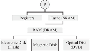
The processor talks directly to the fastest memory module available, which is the registers and the cache memory. The only problem is that these two memory modules do not have a large capacity and are expensive to build.
The interconnection pattern of the memory hierarchy is such that each memory module shown in the figure communicates with the neighboring modules connected to it by the shown lines. Data migrate to the processor from the bottom of the hierarchy. Likewise, data from the processor migrates downwards down the hierarchy. The thickness of each line symbolizes the speed of communication of the line. For example, the processor can directly communicate with its registers and the cache at high speed, matching the clock speed of the processor. Both of these memory components are very fast since they are always implemented on the same chip as the CPU. This ensures speeds that match the processor instruction execution speeds. The goal is to make sure that the processor operates most of the time using only the data and instructions residing in its registers and cache. Whenever the processor needs data or instructions from the memory, things slow down considerably until such data migrate to the cache.
The closest memory to the CPU is the register bank memory, which is built using the same gate technology as the rest of the processor. Hence, registers are very fast and match the processor speed. It is not possible to satisfy all the system storage requirements using registers since a chip has a limited silicon area. Register memory is therefore of small capacity and most computers have a limited amount of registers. For example, Intel’s Itanium processor has 96 registers.
The cache is also very close to the CPU and can communicate with the processor. Similar to registers, the cache communicates at speed matching CPU speed. The cache also communicates with the off-chip dynamic random access memory (DRAM) using slower communication links. A cache is useful because most tasks or applications display temporal locality and spatial locality. Temporal locality refers to the near future. Spatial locality refers to using data stored near the current data. For this reason, data load/store operations between the shared memory and the caches take place using blocks of data. Cache memory is built using static random access memory (SRAM) technology. SRAM is both fast and nonvolatile but also has limited capacity since the number of transistors to store a bit varies between four and six.
DRAM, or memory, is a slower memory but with a large capacity compared with the cache. However, DRAM is considered extremely fast compared with the mass storage disk drives. The problem with DRAM is its volatility. It loses all its content due to current leakage even when power is applied. The entire memory content must be refreshed every 1 millisecond or so. DRAM is slow because it is built on a different chip and its large capacity dictates slow data access operations. In summary DRAM constitutes the main memory of any processor. This memory is inexpensive, slower than cache, but much faster than mass disk storage.
The most inexpensive memory is mass disk storage, whether it uses magnetic storage or optical storage as in CD, DVD, Blu-ray, and so on. Disk storage is inexpensive and has a large capacity. However, it is slow since it is based on mechanical devices. A recent addition to disk storage is electronic disks based on flash memory cards. This is usually referred to as solid state disk or flash drive. Relative to magnetic disks, flash drives are high-speed devices and are starting to have a consistently large capacity. However, their speed does not match the processor speed since they are off-chip memory. We are already seeing advances in flash memory, which possesses most of the desirable features of a memory. It is nonvolatile and fast, and its capacity is increasing with advances in technology.
2.4.1 Cache Memory Operation
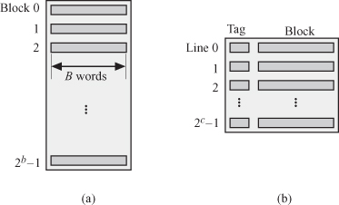
Communication between the main memory and the cache occurs in chunks of words called blocks. Figure 2.4 shows the organization in the main memory and the cache from the point of view of communicating between the two modules. Figure 2.4a shows that the main memory is organized in blocks having B words each. Each block is addressed by a b-bit address so that memory is divided into 2b blocks as far as memory/cache interaction is concerned. Figure 2.4b shows that the cache is organized in lines where each line contains a block from the main memory and an associated tag. The cache capacity is much smaller than the memory and it can store only 2c lines. The tag stores the address of the block in memory corresponding to the line in the cache. This way, a cache line is identified with the corresponding memory block.
Figure 2.4 Cache and memory organization. (a) Memory organization into blocks for communicating with cache. (b) Cache organization into lines.
When the processor requires to read the data, it issues a read instruction and generates the memory address of the word. If the word is in the cache, then we have a cache hit and the word is delivered to the processor at a very high rate. If, however, the processor does not find the word it needs in the cache, then we have a cache miss, and data access halts until the contents of the cache are updated from the main memory. The block containing the word is fetched from the memory and loaded into the cache. The desired word is forwarded to the processor. Communication between cache and memory is performed over blocks of data and progresses at the speed of the DRAM memory access.
2.4.2 Cache Design
We saw that processing speed is high as long as memory read/write operation concerns data and instructions that are located in the cache. Things slow down considerably if the data are not located in the cache. The design of cache memories is beyond the scope of this book, and there are several excellent textbooks dealing with such issues as References 18 and 19. There are several factors that increase the chances of cache hits, which include
- cache size (2c);
- mapping technique to associate the address of a block in memory with the address of a line in the cache;
- cache replacement or update policy; this policy is concerned with choosing blocks of memory to load into the cache and with removing lines from the cache; and
- using cache hierarchy, as will be discussed in the next section.
2.4.3 Cache Hierarchy
Cache memory communicates directly with the processor, and there is always the need to increase the cache capacity to prevent the penalty of cache misses. Since the memory hierarchy model proved very useful in providing the processor with the best of the different storage technologies, it is now common to use the memory hierarchy to construct a parallel model for cache hierarchy. Cache could be organized in different levels. Figure 2.5 shows the different cache levels used to construct a cache hierarchy. Level 1 cache (L1) is an on-chip cache, which is very fast but has a small capacity. This is indicated by the thick line connecting the CPU and the L1 cache. Level 2 (L2) cache is slower than L1 cache since it is off-chip but has a larger capacity. Such memory is built using fast SRAM technology but has a larger capacity compared with the smaller L1 cache.
Figure 2.5 Cache hierarchy.

2.4.4 Mapping Memory Blocks into Cache Lines
A mapping function establishes a correspondence between the main memory blocks and the lines in the cache [19]. Assume we have a memory of size 64 K—that is, the memory address line has 16 bits. Figure 2.6 shows how data are addressed in memory. Figure 2.6a is the case when the memory is organized into words and a memory address specifies a specific word in memory. Sixteen bits are required to specify and access a specific word in the memory.
Figure 2.6 Main memory. (a) Organized into words. (b) Organized into blocks.

Figure 2.6b is the case when the memory is organized into blocks and a memory address specifies a specific block in memory. Assume that each block contains 16 words. The 16 address bits are now broken down into two fields: the most significant 12 bits are required to specify and access a specific block in the memory. The remaining least significant 4 bits specify a word in a given block.
Now assume we have a cache memory that can accommodate 128 blocks. In that case, 7 bits are needed to specify the location of a line in the cache. Now we need a mapping function that picks a block from the memory and places it at some location in the cache. There are three mapping function choices:
1. Direct mapping
2. Associative mapping (also known as fully associative mapping)
3. Set-associative mapping
Direct Mapping
In direct mapping, we take the 12-bit address of a block in memory and store it in the cache based on the least significant 7 bits as shown in Fig. 2.7. To associate a line in the cache with a block in the memory, we need 12 bits composed of 7 bits for address of the line in the cache and 5 tag bits.
Figure 2.7 Direct-mapped cache.
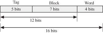
Now we see that a line in the cache corresponds to 32 blocks from the main memory, which correspond to the 5-bit tag address. This is because there are exactly 32 blocks in the main memory whose least significant 7 bits are all identical out of the 12-bit line address.
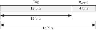
2.4.5 Associative Mapping
In associative or fully associative mapping, we place the block of memory in any available location in the cache, in this case, the tag is used to associate a block with a line as shown in Fig. 2.8. To associate a line in the cache with a block in the memory, we need 12 bits composed of the 12 tag bits (Fig. 2.8).
Figure 2.8 Associative mapped cache.
2.4.6 Set-Associative Mapping
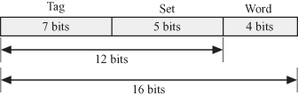
Set-associative mapping could be thought of as a combination of direct and associative mapping. We divide the cache into 2m sets and associate a block to a set based on the m least significant bits of the block address bits. The block is mapped to any empty location in the set. For a cache with capacity of 128 blocks, if we divide the cache into 32 sets, we would be able to store four blocks per set. The breakdown of the 12-bit block address is shown in Fig. 2.9. To associate a line in the cache with a block in the memory, we need 12 bits composed of 5 bits for the address of the set in the cache and 7 tag bits.
Figure 2.9 Set-associative mapped cache for the case of dividing the cache into 32 sets.
2.4.7 Effects of Cache Size on Cache Misses
Cache misses can be classified into three categories (the three Cs) [20]:
Compulsory misses: caused when a block is initially required but has never been loaded into the cache. This type of cache miss is also called cold-start miss. Cache size has no effect on compulsory misses.
Capacity misses. Caused when the cache cannot hold the blocks needed during the execution of a program. In that case, blocks are replaced then later loaded back into the cache. Capacity misses are reduced by enlarging the cache size.
Conflict misses: Occur in set-associative or direct-mapped caches when the cache cannot accommodate the blocks in a set. Such misses would not have occurred in a fully associative cache. Conflict misses are also called collision misses. Conflict misses are reduced by increasing the associativity or by increasing the number of lines to map to in the cache. This can be accomplished either by increasing the cache size or by reducing the block size.