13
Semiconductors: And Their Junctions
13.1 Introduction
In this chapter, we will examine semiconductors, diodes, transistors, and other components that changed electronics forever.
13.2 It All Started with a Light Bulb
A light bulb is composed of a filament inside a vacuum glass enclosure. This filament is made of a heat‐resistant material, like tungsten, that can become incandescent for long periods of time without melting.
The incandescence produces light and emits a cloud of electrons around the filament.
Figure 13.1 shows a light bulb with an incandescent filament and a cloud of electrons, represented by orange circles with the minus sign.
Electrons are negative charges. What would happen if a metallic plate was added to the light bulb and charged with a positive charge? Remember that opposite charges attract themselves.
Figure 13.2 shows a light bulb with a metallic plate at the opposite end. The metallic plate is connected to the positive of a couple of batteries in series.

Figure 13.1 A light bulb.

Figure 13.2 A primitive vacuum tube.
As expected, the positive plate will attract the electrons from the filament cloud. The bigger the plate’s positive charge, the more intense is the force attracting the electrons from the cloud.
If we make the plate negative, instead of positive, it will repel the electrons from the cloud, because charges with the same polarity repel each other.
A new component was created: the vacuum tube or simply known as tube or valve (in the United Kingdom).
If we have electrons moving from one element to the other, we have current flow in the opposite direction.
However, notice that the electrons move from the filament to the plate and not the other way around. Consequently, current can only move in one direction. If so, we have this device that allows current to flow in one direction (when the anode is positive) but not to the other (when the anode is negative). A new component is born: the diode.
Figure 13.3 shows the diode symbol for the vacuum tube, where anode, cathode, and heater can be seen from top down.
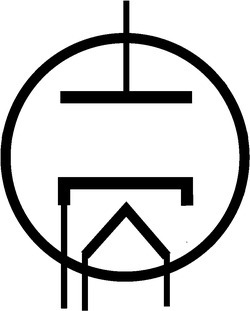
Figure 13.3 Diode symbol (vacuum tubes).
The next step on the vacuum tube evolution was placing a metallic grid between the anode and the cathode to control the flux of current between these two elements.
This grid, also called control grid, could be made positive or negative, blocking or letting pass electrons.
A new component was born: the triode.
Figure 13.4 shows the symbol for the triode, where the anode, the grid, the cathode, and the heater can be seen from top down.

Figure 13.4 Triode symbol (vacuum tubes).
13.3 Semiconductors
During the Second World War, vacuum tubes were used as the central element of electronic circuits.
Tubes did the job relatively well, but they were fragile and required high voltages to work – not to mention they require a lot of current and power to operate and their filaments do not last that long.
In 1948, William Shockley, researcher at the legendary Bell Labs, invented something he called “circuit element utilizing semiconductive material”, the basis of what we call, today, transistor.
13.3.1 Bipolar Junction
The first transistors were made of germanium (Ge). Today, transistors are made of silicon (Si).
Silicon is a hard and brittle crystalline solid with a blue‐gray metallic luster and is classified chemically as a metalloid. Metalloids are chemical elements with properties intermediate between those of typical metals and nonmetals.
Every silicon atom contains four electrons in their valence shell, as illustrated in Figure 13.5.
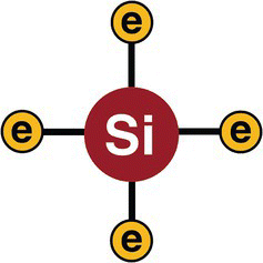
Figure 13.5 A silicon atom.
When a structure of silicon is formed, every atom bonds to its neighbor by sharing one electron from the valence shell. This kind of bond is known as covalent bond, represented in Figure 13.6.
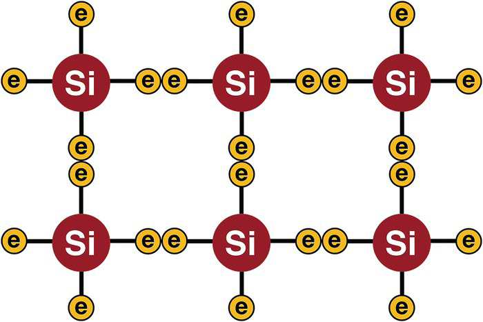
Figure 13.6 Silicon structure.
In a structure like this, all electrons are combined to their neighbors, and there are no free electrons to move. This kind of structure can be classified as an insulator with a very high electrical resistance or as an element with a very little electrical conductivity.
13.3.1.1 Making the Structure More Negative
To make a silicon structure a better conductor, we must add more electrons to it.
The solution was to add phosphorus atoms to the silicon structure.
Phosphorus atoms contain five electrons on their valence shell (Figure 13.7).
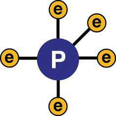
Figure 13.7 Phosphorus atom.
The technique of adding phosphorus to the silicon structure is called doping. The result is represented in Figure 13.8.
It is now clear that each phosphorus atom will add a free electron to the structure. Millions and millions of these free electrons will now be embedded in the silicon structure, increasing its conductivity.
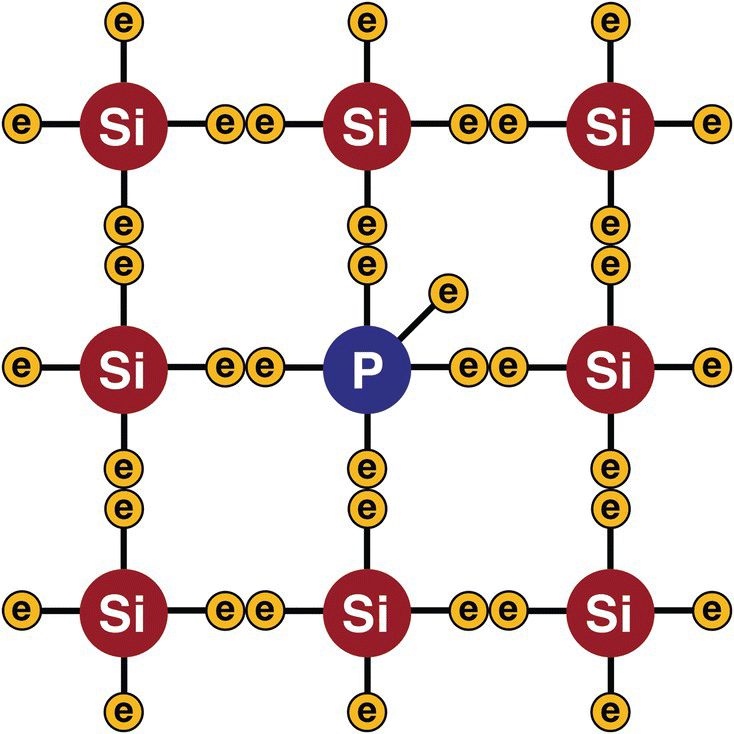
Figure 13.8 N‐type silicon structure.
13.3.1.2 Making the Structure More Positive
Boron atoms, on the other hand, differently from phosphorus, have just three electrons on the valence shell. See Figure 13.9.
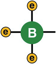
Figure 13.9 Boron atom.
If we take silicon and dope it with boron, instead of phosphorus, we will create a structure that have empty spots, like holes, that represent “parking spots” for electrons. In other words, a structure that lacks electrons consequently is less negative or more positive (see Figure 13.10).

Figure 13.10 P‐type structure.
13.3.1.3 Pure Magic
Something magical happens when we put together an N‐type and a P‐type block of silicon: the excess of electrons from the N‐type block migrates to the P‐type block, at the junction between the two materials. This will make the N‐type material less negative and the P‐type material more negative, at the border.
Figure 13.11 shows both materials put together, P‐type and N‐type, and the depletion region formed at their junction.
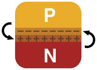
Figure 13.11 PN junction.
This will create a permanent electric field at the junction, a barrier that will make impossible the migrations of more electrons. This barrier is known as depletion region and represents an insulation barrier between the two materials.
In other words, the barrier existence means that current will only flow across the junction where a voltage potential greater than the barrier potential is applied.
13.3.1.4 Reverse Biasing
If we connect the positive and negative poles of a battery to the N‐type and P‐type blocks of a PN junction, respectively, we will increase the depletion region size.
The battery will polarize the blocks in such a way that more holes from the P‐type will be attracted to the negative pole and electrons from the N‐type will be attracted to the positive pole, enlarging the depletion barrier, raising the barrier’s electric potential, and making current circulation impossible. See Figure 13.12. This is called reverse biasing.
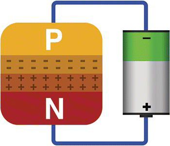
Figure 13.12 PN junction – reverse biased.
13.3.1.5 Forward Biasing
If, on the other hand, we invert the battery, we will decrease the barrier potential by attracting electrons from the P‐type into the N‐type. The battery will force the barrier to contract. In this case, current will flow as soon as the battery can provide a potential bigger than 0.7 V (see Figure 13.13). This is called forward biasing.

Figure 13.13 PN junction – forward biased.
13.3.1.6 Biasing Curve
The previous description of a junction that can block current flow when reverse biased and allow current flow when forward biased represents the ideal case. In real life, imperfections will prevent junctions to behave like that.
If we forward bias a PN junction using a variable power supply, starting with 0 V and gradually increasing the voltage, the junction barrier will be contracted to a point where it will start to conduct, and this will happen when the power supply is providing around 0.7 V. This is shown in region A in Figure 13.14.

Figure 13.14 PN junction biasing curve.
Point Vd is a point beyond which the junction will start to conduct from the P‐type to the N‐type.
If we invert the power supply and gradually start to increase the voltage, the junction that should block current at all costs will not resist and let current flow, but in the opposite direction, from the N‐type to the P‐type. Current is negligible, near zero, on the order of microamperes. See region B on Figure 13.14.
If we continue to increase the power supply, keeping the power supply reversed, at some point, the junction will not resist and fail catastrophically, letting current pass at full blast, in the opposite direction. This point is called breakdown voltage or avalanche voltage and is marked as Vbr on region C in Figure 13.14.
13.3.1.7 Thermal Voltage
Atoms are constantly vibrating inside the silicon structure and this vibration produces heat.
If we subject the material to low temperatures, for example, 0 K, all vibrations stop.
As temperature rises, electrons acquire energy, start to vibrate, and become available to move freely across the structure. This proportion of free electrons and temperature is ruled by the Boltzmann constant.1
This vibration has a direct relation with temperature and generates an electric potential, called thermal voltage (VT), expressed by the next formula.
Conversion from Celsius to Kelvin can be calculated by the following formula.
The thermal voltage for a room temperature of, for example, 300 K would be calculated as
13.3.1.8 Barrier Voltage
The famous barrier voltage of the PN junction being equal to 0.7V comes from the following formula.
13.3.1.9 Relation Between Current and Voltage
The relation between current and voltage across a PN junction, or diode, is expressed by the following formula, known as the “diode equation.”
Notes
- 1 Equal to
 (Joules per Kelvin), in honor to Ludwig Eduard Boltzmann, an Austrian physicist and philosopher who developed a theory that explains and predicts how the properties of atoms determine the physical properties of matter. The Boltzmann constant was modified recently by the SI. This value was previously equal to
  .
. - 2 The electron charge value was modified recently by the SI. This value was previously equal to
 .
.