29
Transistor Amplifiers: The Magic Component
29.1 Introduction
In this chapter, we will examine the usage of transistors as amplifiers.
We will show how transistors are able to “amplify”1 signals and will briefly introduce the reader to how they work.
29.2 Transistor as Amplifiers
Nothing is farther from the truth than thinking transistors are magical devices that can amplify the signals they receive, like a magical portal that receives the signal and amplifies it.
In fact, transistors are like switches that can manipulate and modulate the voltage coming from the power supply to generate a huge copy of the input signal, creating the illusion of amplification.
The output signal is not the input signal amplified but rather the power supply voltage modulated to look like the input signal.
29.3 The Water Storage Tank
Imagine a huge water store tank with a large output pipe. At the bottom of the tank, a tiny water valve is connected electronically to a huge water valve that opens or closes the main pipe. Therefore, if you rotate this tiny valve to one direction, it will make the huge water valve open and let a gigantic amount of water exit from the tank. If you rotate the tiny water valve to the other direction, the huge valve will close.
Thus, small rotations of the tiny valve will produce huge rotations of the largest valve.
This can be interpreted as an amplification: a small rotation producing a large rotation.
This is what roughly happens with transistors: a tiny current flowing into the input will produce a large current flowing across the output.
29.4 Current Gain
If the reader remembers what we have explained previously about transistors, a transistor, which symbol for an NPN type is shown in Figure 29.1, is a three‐terminal device, with a collector (C), a base (B), and an emitter (E).
In an NPN type transistor, a small current flowing from the base to the emitter (base current) will produce a larger current flowing from the collector to the emitter (collector current). This effect is known as “current gain,” also known as transistor hFE or β.

Figure 29.1 NPN transistor.
Different transistors offer different values for the current gain, which can vary from 10, 20, and 50 to values like 800.
Therefore, the collector current will be the base current multiplied by hFE, or
29.5 Power Supply Rails
All electronic circuits are powered by some kind of voltage source. The voltage source can be a battery or an electrical device of some kind.
Suppose this voltage source is a 9 V battery. This battery has a positive and a negative pole. These two poles or voltage limits are known as rails.
In an amplifier, the output should never exceed the rails or distortion will appear at the output, and damage can happen to the power supply.
29.6 Amplifying
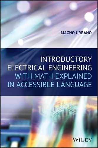
Suppose we want to amplify a sinusoidal wave like the one shown in Figure 29.2. This wave varies from 1 V to −1 V; therefore, this is a 2 V peak‐to‐peak voltage, or 2 Vpp. This means the audio signal varies between positive and negative values.

Figure 29.2 2 Vpp audio signal.
Suppose our amplifier is powered by a 9 V battery. If this is the case, the maximum output signal we can collect at the output, in theory, will be a 9 Vpp signal, as shown in Figure 29.3.
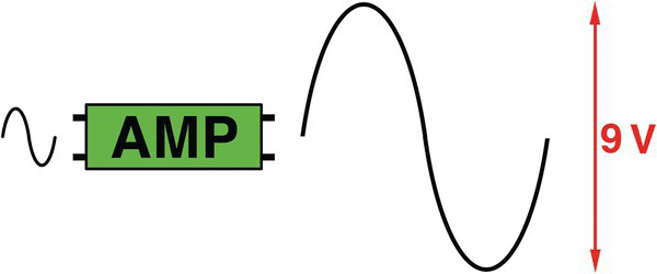
Figure 29.3 Input signal and maximum output possible.
This happens because the amplifier output is limited by the power supply voltage.
Therefore, for an input signal of 2 Vpp, the amplifier will only be able to amplify the signal 4.5 times to get a 9 Vpp output.
When the output varies the full range possible, in this case from the battery negative pole or 0 V to the maximum battery voltage, or 9 V, equivalent to the battery positive pole, it is said that the output does a full swing or full rail, going from the minimum to the maximum rail, provided by the power supply.
29.7 Quiescent Operating Point
To work as an amplifier, a transistor must be configured properly to operate within a certain range of parameters. This operating point is called “quiescent operating point” or “Q‐point.”
Adjusting the operating point of a transistor is called biasing.
Suppose a transistor amplifier will be used to amplify audio signals. An audio signal has positive and negative values. If our amplifier is powered by 9 V battery and the output cannot go beyond this value, we must bias the transistor in a way that the output sits at 4.5 V, the middle of the rail, when there is no input signal. By biasing the transistor like that, the output will be able to swing from 4.5 to 9 V during the output positive cycle and from 4.5 to 0 V during the negative cycle (see Figure 29.4).

Figure 29.4 Input and output signals.
29.8 Amplifier Classes
Transistors can be used to create amplifiers in very different ways, called “classes.” Every class is more or less energy efficient than another.
These classes are named with letters, like A, AB, B, C, D, E, F, G, H, S, and variations of B.
The simplest class of them all is class A and, for that reason, will be the theme of this chapter, specifically in a configuration called common emitter, as we will examine later in this chapter.
29.8.1 Class A
Class A amplifiers are probably the cheapest and the simplest to produce.
Class A amplifiers are good amplifiers with a relatively low output distortion.
The problem with class A is that it consumes too much power. The transistors in a class A configuration are always conducting current, meaning that they are consuming power even if there is no signal at the input.
Therefore, they are not the best amplifiers to use in portable devices, powered by batteries.
To improve the energy efficiency of class A amplifiers, engineers created other classes that improve the energy problem, but these new classes introduce other problems, like signal distortion.
29.8.1.1 Common Emitter
To make a transistor work as an amplifier, it must be properly biased.
Biasing a transistor means adjusting its voltages and currents, so it can operate as an amplifier.
Common‐emitter mode is the most popular way to use a transistor as an amplifier.
It is called “common‐emitter” amplifier since the emitter is common to both the input and the output circuit.
Common‐emitter amplifiers have the following characteristics:
- Signal enters by the base and exits by the collector.
- Medium input and output impedances.
- Medium current and voltage gains.
- High power gain.
- Input and output have a phase relationship of 180°.
29.8.1.1.1 Biasing a Transistor
Biasing a transistor to work as a common‐emitter amplifier can be done in three basic ways: fixed base biasing, collector feedback biasing, and voltage divider biasing.
We will examine these configurations in the next sections.
Fixed Base Biasing
This method for biasing a common‐emitter class A amplifier is seen in Figure 29.5.
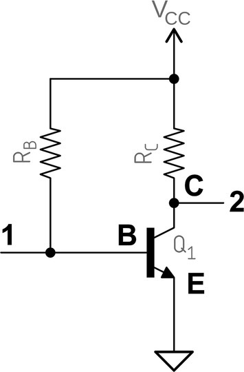
Figure 29.5 Fixed base biasing common‐emitter amplifier.
In Figure 29.5, VCC represents the power supply’s positive pole, and the triangle pointing down, known as the ground point, represents the power supply’s negative pole. RC is the collector resistor and RB is the base resistor.
This fixed base biasing configuration uses a resistor connected between VCC and the collector and another one from the same point to the transistor base. The purpose of these resistors is to provide voltage levels and currents for the transistor operation. The emitter is connected to the ground, as shown in Figure 29.5.
Figure 29.6 Currents and voltages in a fixed base biasing common‐emitter amplifier.
In the common‐emitter configuration, the input signal enters by the transistor base, point 1 in Figure 29.5, and exits by the collector (C), or point 2. Therefore, the input signal will be connected between point 1 and ground, and the output will be collected between point 2 and ground.
To set the operating point for the fixed base biasing configuration, we start by specifying the currents. Figure 29.6 shows the several currents of this kind of configuration: the collector current (iC), the base current (iB), and the emitter current (iE).
Figure 29.6 also shows the voltage across collector–emitter (VCE) and the voltage base–emitter (VBE).
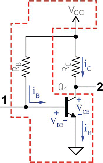
Figure 29.7 Input mesh of a fixed base biasing common‐emitter amplifier.
Figure 29.6 shows that the base is positive compared with the emitter, meaning that the base must have a greater electrical potential. In fact, to work properly, the voltage at the base must be at least 0.7 V greater than the emitter. If so, current will flow from collector to emitter.
The signals of VCE in Figure 29.6 show that the voltage at the collector will be greater than the emitter during normal operation.
Currents
We start by applying Kirchhoff’s voltage law (KVL) to the circuit’s input mesh shown in Figure 29.7, composed of the base resistor, the power supply, and the base–emitter junction.
This mesh is equivalent to the circuit shown in Figure 29.8.
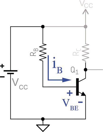
Figure 29.8 Equivalent input mesh of a fixed base biasing common‐emitter amplifier.
If we apply KVL to this mesh, we get
Therefore, we can find the base current by rearranging the equation
We know that the collector current is

Figure 29.9 Output mesh of a fixed base biasing common‐emitter amplifier.
In the next step, we find the voltage across collector–emitter by applying KVL to the output mesh, shown in Figure 29.9.
This output mesh is composed of the collector resistor, the collector–emitter block, and the power supply, as shown in Figure 29.9, and can be redrawn as shown in Figure 29.10.
If we apply KVL to this mesh, we get
Therefore,

Figure 29.10 Output mesh equivalent of a fixed base biasing common‐emitter amplifier.
and
A transistor can be one of three states, namely, cutoff, saturated, or conducting, this later being equal to the normal operating mode as an amplifier.
If a transistor is saturated, the collector–emitter voltage, VCE, will be 0. Therefore, current will be flowing at maximum intensity, just limited by the collector resistor.
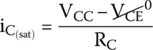
In this case, the saturation collector current will be
On the other operation extreme, or when the transistor is cutoff or not conducting, VCE will be equal to the power supply voltage, VCC, because there is no current flowing across the collector; therefore,
If we want the transistor to work correctly as an amplifier, we must make sure that it operates in the middle point between saturation and cutoff in what is called the “active region.” We also have to be sure that the input signal does not drive the circuit out of this region.
Setting It Up
We will set this project to use the low power general‐purpose silicon‐based transistor model 2N2222A and to be powered by a 9 V battery.
Transistor manufacturers publish datasheets about their products where the electric characteristics of their devices are specified at detail. The datasheet for transistor 2N2222A is available at MIT.
You can access their document using our shortcut at http://transistor.katkay.com
The datasheet shows the collector–emitter saturation voltage curve, shown in Figure 29.11.
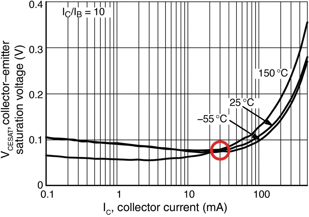
Figure 29.11 Collector–emitter saturation voltage for transistor 2N2222A.
This graph shows that the collector–emitter voltage keeps its value relatively stable until the collector current reaches about 30 mA. After that, its values increase exponentially. Therefore, we must choose a collector current that is below 30 mA to keep the transistor operating in a stable region. We choose 10 mA for this project.
We read the datasheet again and this time we look for the current gain curve (hFE), shown in Figure 29.12.

Figure 29.12 Current gain curve for transistor 2N2222A.
Figure 29.12 shows a value for the hFE parameter equal to 225 for a current of 10 mA at room temperature.
Thermal Runaway
Figure 29.12 shows three curves for hFE, one for each different temperature. The higher the temperature, the bigger the hFE value, making it clear that hFE increases when the temperature rises.
A transistor will normally heat during normal operation due to the current flowing between collector and emitter. This temperature rise will increase the hFE value. The collector–emitter current is product of the base current and the hFE. If hFE rises, the collector–emitter current will increase and so on, which can lead to the transistor destruction.
This effect is called “thermal runaway,” and the best way to prevent this situation is to add a resistor between the emitter and the ground, something that this circuit lacks.
The lack of an emitter resistor in this circuit is condition enough not to use this kind of project, but we will show other situations that makes this, in this fixed base biasing method not good as an amplifier.
We have established four values for our amplifier design so far: the power supply voltage, the collector current, the current gain, and the base–emitter voltage:
The ideal amplifier would be the one that can provide a full swing output. In this given example, it would be an amplifier that could provide an output varying from 0 to 9 V.
But like we have explained before, a few conditions will prevent an amplifier from using the full rail. One of these conditions is the collector–emitter voltage.
Reading the graph in Figure 29.11, we see that the transistor 2N2222A has a collector–emitter saturation voltage of, approximately, 0.1 V for 10 mA. As a rule of thumb, we think that it is too dangerous, in terms of transistor stabilization, to have a collector–emitter voltage below 0.7 V, and we recommend always having it bigger than 1 V.
To make sure we will have a stable amplifier, we will choose to have this minimum voltage set to 2 V through this chapter. Therefore, the minimum collector–emitter we choose is
The emitter is connected to the ground, as we can see in Figure 29.9. Consequently, 2 V is also the minimum collector voltage, or in other words, the collector voltage when the output is at its minimum value.
The collector is where the signal output exits, meaning that the output is collected between collector and ground.
We have just selected 2 V as the minimum voltage for the collector, meaning that no collector voltage must be below that point. That is the same as saying that the amplifier will only be able to vary from 2 to 9 V. Therefore, the larger output signal may have only the difference between these two values, that is, 7 V peak to peak.
Consequently, the output wave will only be able to vary by 3.5 V up and the same amount down.
If the maximum allowable voltage for the collector is 9 V, then it must be adjusted to be 3.5 V below that point when at rest, equivalent to 5.5 V = 9 − 3.5, a voltage we call “middle point collector voltage,” or “collector at rest voltage,” which can also be found by the following formula:
or
Therefore,
Now the output can swing 3.5 V up, from 5.5 to 9 V during the positive cycle and 3.5 V down, from 5.5 to 2 V during the negative cycle.
Resistors
We must calculate, now, the resistors that will make every chosen voltage and current possible.
This is what we have chosen so far:

We can start by finding the collector resistor by using Eq. (29.3):
We can use Eq. (29.2) to find the base current:
But we also know by Eq. (29.1) that
and we can use this equation to find the base resistor:
AC Analysis
What happens to the circuit when an audio signal is applied to the input?
First, we must remember that the way we have designed this amplifier was in such a way to establish the currents flowing in the transistor, the base voltage as 0.7 V and the collector voltage at rest, to be at 5.5 V.
Suppose we now inject a sinusoidal audio signal at the transistor base, like the one shown in Figure 29.13. This signal can be from a microphone, for example, and varies from +40 to −40 μA.

Figure 29.13 Audio signal.
The Positive Cycle
At the beginning, the audio signal sits at 0 μA (see Figure 29.13). Therefore, there is no current injected at the transistor base, and all other currents or voltages in the circuit keep their calculated values.
As time passes, the audio signal increases from 0 μA and reaches its peak at +40 μA.
We have calculated the base current to be 44.44 μA, but now, there is this new additional current of +40 μA coming from the audio signal, making the base current increase to 84.44 μA.
This new base current will make the collector current increase to
In other words, the collector current increased from 10 to 19 mA.
If we go back to the output mesh’s KVL equation and solve for VCE, using this new collector current, we get the new collector–emitter voltage:
In resume, during the positive cycle of the audio signal, it varied from 0 to +40 μA, making the base current increase from 44.44 to 84.44 μA, forcing the collector voltage to vary from 5.5 to 2.35 V.
In other words, an increase in the input current produced a decrease in the output voltage, showing that this amplifier is an inverter, meaning that all signals injected at the input will be collected at the output inverted, with a 180° phase offset.
The Negative Cycle
In this section we will see what happens during the negative cycle of the audio input.
The time passes and the audio signal decreases to −40 μA. This new negative current is added to the base current, making it drop from 44.44 to only 4.44 μA.
This new current will produce the following collector current:
If we go back again to the output mesh’s KVL equation and solve for VCE using this new current, we get
In resume, the audio signal varied from 0 to −40 μA, making the base current drop from 44.44 to 4.44 μA, forcing the collector voltage to vary from 5.5 to 8.65 V.
In other words, a decrease in the input current produced an increase in the output voltage, confirming this amplifier as an inverter.
Conclusion
This fixed biased transistor amplifier works as an amplifier within certain parameters, but it is rarely used in real life because it has a lot of problems.
The first problem is lacking an emitter resistor, which can lead the transistor to self‐destruction, for the reasons we have explained.
The other problem is that the design is highly dependable on the hFE value. In real life, even the same type of transistor can have different values for hFE. The slightest difference in hFE will result in different voltages and currents across the circuit.
To see the dependence of hFE of this kind of circuit, consider the voltage gain of this amplifier.
The voltage gain will be the output voltage divided by the input voltage.
Looking at Figure 29.6, we can see that the output voltage is
and that the input voltage is
Thus, the voltage gain is
We have iC and iB in the formula and we know that
Therefore, the voltage gain is
You can see that hFE is in the voltage gain formula and that iB is in both nominator and denominator, making the voltage gain dependent on these values.
Even the same kind of transistor hardly has the same hFE. Imagine designing a product to be sold to thousands of customers that behave differently for every person.
With this kind of design, voltages and currents do not remain stable during transistor operation and can vary enormously, and even if the transistor does not self‐destruct, due to the thermal runaway problem, its temperature will affect and change hFE, increasing the output current and disturbing all other voltages and currents across the circuit.
For all these problems, this circuit design is not recommended.
In the following section, we will examine other types of transistor biasing and see if we can solve this problem.
Collector Feedback Biasing
Figure 29.14 shows a collector feedback biasing circuit where RC is the collector resistor and RB is the base resistor or the feedback resistor. The base resistor is connected to the collector, instead of being connected to the power supply.
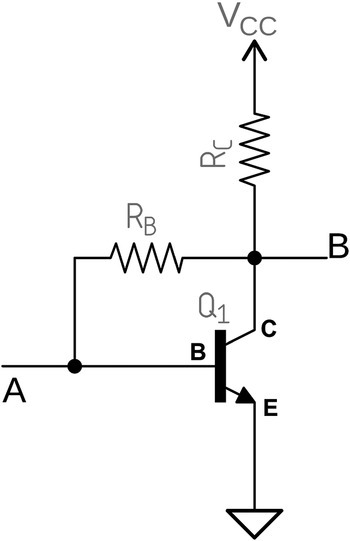
Figure 29.14 Collector feedback biasing.
This situation creates what is called collector feedback. The word feedback is used because part of the collector current is injected into the base. The collector feedback current ensures that the transistor is always biased in the active region.
Like we have seen previously, when the collector current increases, the voltage at the collector drops, because the voltage drop across the collector resistor increases. This reduces the base current that in turn reduces the collector current and so on until it stabilizes at a certain value.

Figure 29.15 Collector feedback biasing (currents).
We will see in the next paragraphs that this kind of amplifier design is also an inverter amplifier.
This feedback resistor is, in fact, creating a negative feedback into the input, because part of the inverted output signal is being injected into the input.
There are several benefits of negative feedback in any kind of amplifier like improving system stabilization, reducing distortion and noise, and improving the system bandwidth. However, a reduction in gain is present for all amplifiers using feedback.
Currents
The first thing is to establish the currents flowing in the circuit, like shown in Figure 29.15.
By the diagram in Figure 29.15, we can establish that
We know that
Therefore, current across RC will be
Consequently, voltage drop across RC is

Figure 29.16 Input mesh of a collector feedback biasing circuit.
If we apply KVL to the input mesh (Figure 29.16), formed by the collector and the base resistor and the base–emitter junction, we get
which means that the power supply voltage subtracted from the voltage drops across the collector and the base resistors subtracted from the base–emitter voltage is equal to 0.
This can be expanded into
Upon substituting (29.4),
Therefore, the base current will be
Figure 29.17 Output mesh of a collector feedback biasing circuit.
If we apply KVL to the output mesh (Figure 29.17), formed by the collector resistor and the collector–emitter block, we get
This can be expanded into
Upon substituting (29.4),
Therefore,
By comparing the base current (29.5) and the collector current (29.6), it is clear that both the collector and the base currents are highly dependable upon hFE.
To see the dependence of hFE of this kind of circuit, consider the voltage gain of this amplifier.
The voltage gain will be the output voltage divided by the input voltage.
Looking at Figure 29.6, we can see that the output voltage is
and that the input voltage is
Thus, the voltage gain is
We have iC and iB in the formula and we know that
Therefore, the voltage gain is
You can see that hFE is in the voltage gain formula and that iB is in both nominator and denominator, making the voltage gain dependent on these values.
This design shows the same problem as the fixed base biasing one: currents and voltages will vary wildly if hFE changes. An additional issue with this design is the lack of an emitter resistor to prevent the thermal runaway problem.
We must continue our epic journey to find another biasing method that can solve these problems.
29.8.1.1.2 Voltage Divider Biasing
This method of transistor biasing is shown in Figure 29.18, known as voltage divider biasing, and is the most popular method of biasing a transistor.
In this kind of biasing, RC is the collector resistor and RB is the base resistor.
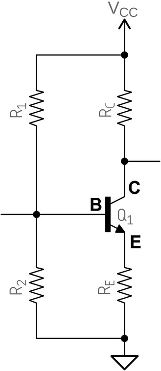
Figure 29.18 Voltage divider biasing.
R1 and R2 are called the bias resistors, configured as a voltage divider that runs a large current across, compared with the base current, and helps to establish a stable base voltage and minimize any variations in the base current.
The thermal runaway problem is finally solved by adding an emitter resistor.
The emitter resistor RE is, in fact, the sum of two resistors: the emitter resistor RE itself and a resistor we will call “gain resistor,” proper from the transistor, that controls the voltage gain or the amplification factor. We will disregard this resistor in this book because it falls outside the book’s objective.
Parameters
The first thing we must do is to establish the transistor operating point.
We have added an emitter resistor to solve the thermal runaway. A current will flow across this resistor and cause a voltage drop. Therefore, the emitter (Figure 29.18) will have a voltage that is not 0, like the previous designs we have examined, because the emitter is not connected to the ground anymore.
If our intention is to make an amplifier with the maximum output voltage swing possible, we must choose a value for the emitter voltage that is the lowest we can get, because this voltage will reduce the output swing by the same amount.
Remember when we first examined this that the possible output voltage range is VCC subtracted from the collector–emitter voltage. Now with another voltage drop on the output mesh, the maximum output range possible will be VCC subtracted from the collector–emitter voltage and the emitter resistor voltage drop.
It is recommended to have the voltage drop across the emitter resistor around 1 V.
Like the last time, we chose a collector current of 10 mA, which will result in a value for hFE equal to 225 for transistor 2N2222A.
This transistor is silicon based; therefore, its required base–emitter voltage is 0.7 V.
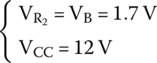
We will use a 12 V power supply for this project, instead of a 9 V battery.
These are the parameters we have so far:


Figure 29.19 Voltage divider biasing (currents).
Currents
Figure 29.19 shows the currents flowing in the voltage divider biasing circuit.
To find the current equations, we start by defining the circuit’s input and output meshes, shown in Figure 29.20.
By applying KVL to the input mesh, we get
Doing the same for the output mesh, we obtain

Figure 29.20 Voltage divider biasing (input and output meshes).
Design
Like the previous project, the collector needs a minimum voltage that is recommended not to be less than 2 V.
Therefore,
If the emitter voltage was chosen to be 1 V and ![]() is 2 V, then the collector minimum voltage will be the sum of these two values, or
is 2 V, then the collector minimum voltage will be the sum of these two values, or
This means that the output voltage will not be able not to vary from 0 to 12 V but rather from 3 to 12 V.
Therefore, to have maximum output amplitude, we must set the collector voltage to be at the middle of this range, or in the middle value between 3 and 12 V, or
Consequently, the output voltage will be able to vary from 7.5 to 12 V during the positive cycle and from 7.5 to 3 V during the negative cycle, a 4.5 V variation for both sides.
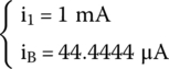
We have the collector current and hFE; therefore we can find the base current:
The emitter current is equal to the sum of collector and base currents, but because the base current is infinitely less than the collector current, we can ignore it and say that, for most purposes, the emitter current is equal to the collector current.
However, in this book, we will always consider the base current.
Therefore, the emitter current is
Knowing these values, we can find the emitter resistor:
Similarly, the voltage drop across the collector resistor is
The collector voltage is also equal to the sum of the voltage across the collector–emitter and the voltage across the emitter resistor, or
If we substitute this in the output mesh equation in equation (29.8), we get another way to represent the voltage across the collector resistor:
which is the power supply voltage subtracted from the collector voltage we have already established before.
Therefore, because Eqs. (29.9) and (29.10) represent the same thing, we can equate them and find the collector resistor:
The bias resistors R1 and R2 are configured as a voltage divider.
Current i1 flows across R1, and a current i2 flows across R2 (Figure 29.19).
Current i1 will be the sum of the base current iB with i2, or
What this means is that the base current will be a fraction of the current flowing across R1. In other words, the base current is drained from the current flowing across R1.
We must consider that the currents across R1 and R2 will establish a voltage divider that will establish the base voltage. Therefore, if we want this base voltage to be as invariable as possible, knowing the base current will be drained from the current i1 across R1, we must choose a value for i1 that is much larger than the base current. This will make sure that the base current being drained from i1 will not disturb the voltage set by the divider.
As a rule of thumb, we generally choose i1 to be 10 times smaller than the collector current iC, or
We already know the collector current. Therefore, we can calculate i1:
We know that the base voltage will be equal to the sum of the emitter voltage and the base–emitter voltage, which, for silicon‐based transistors, is approximately equal to 0.7 V.

Figure 29.21 Voltage divider biasing – The base.
We also know the emitter voltage; therefore, we can find the base voltage:
In Figure 29.19, we see that the base is connected between resistors R1 and R2, as shown in Figure 29.21.
Resistor R2 is connected between the base and ground. The voltage across this resistor is equal to the product of its resistance and current, which is also the base voltage in relation to ground, or
We have two equations for VA. Consequently we can equate them:
We already know that
and
Therefore,
We can now find R2:
Substituting

To find R1, we go back to the input mesh equation:
We already know that
Therefore,
We already know i1, and therefore we can find R1:
In resume, these are the values we have designed so far:
However, when choosing components like resistors, capacitors, inductors, and so on, we must rely on values that are available for sale on the market and some of the calculated values are not.
Checking Appendix G, we choose the final values for 20% tolerance resistors:

These new values will change voltages and currents across the circuit. By the end of this chapter, at the exercises section, we will examine the effect of such changes.
29.8.1.1.3 Conclusion
One thing that should be observed about the voltage divider method is that the base current and the base voltage depend basically on the currents circulating through R1 and R2 and the voltages established by these resistors are independent from hFE.
To see the dependence of hFE of this kind of circuit, consider the voltage gain of this amplifier.
The voltage gain will be the output voltage divided by the input voltage.
Looking at Figure 29.19, we can see that the output voltage is
and the input voltage is
Therefore, the voltage gain is
We do not see hFE on the voltage gain formula because there is no dependence on the base current too, showing how the gain is independent from hFE.
Exercises
- Consider the voltage divider biasing common‐emitter class A amplifier shown in Figure 29.22.
The circuit uses the NPN silicon‐based low power general‐purpose transistor type 2N2222A.

Figure 29.22 Voltage divider biasing.
Figure 29.23 shows the hFE curve for this transistor.

Figure 29.23 hFE DC current gain (transistor 2N2222A).
The power supply voltage and the collector current should be

Design this amplifier for maximum output swing possible.
Solutions
The first thing we do is to define a voltage for the emitter. This will be the voltage across the emitter resistor and as a rule of thumb should be around 1 V to keep the amplifier stable and prevent the thermal runaway.
The current collector was chosen to be 8 mA. This value gives us a value of hFE equal to 225 for this 2N2222A transistor.
This is a silicon transistor; therefore, the base–emitter voltage is approximately 0.7 V.
These are the values we have so far:

The base current can be calculated:


We have chosen the emitter voltage to be 1 V. As a rule of thumb, we know that the collector–emitter voltage should be at least 2 V to keep the transistor out of the saturation zone:
Therefore, the minimum value for the collector voltage during the negative cycle of the output will be


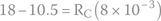
This means that the collector will be able to swing from 3 to 18 V and consequently will have an amplitude of 15 V peak to peak, equivalent to the subtraction of 18 and 3 V.
Therefore, for maximum swing, we must position the collector voltage at a middle point between 3 and 18 V, or


The collector sitting at 10.5 V will be able to swing from 10.5 to 18 V during the positive cycle and from 10.5 to 3 V during the negative cycle of the output signal.
The emitter current is the sum of the collector current and base current, or


Now we can find the emitter resistor:


Similarly, the voltage drop across the collector resistor is

and is also

Therefore, we can equate these two equations and find the collector resistor:

R1 and R2 are a voltage divider. As a rule of thumb, the current across R1 should be 10 times less than the collector current.
We can use this to get the current across R1:


We have defined the voltage across the emitter resistor to be 1 V.
We know that the voltage across base–emitter, for silicon‐based transistors, is around 0.7 V.
Therefore, we can find the base voltage:


R2 is connected between the base and ground. Therefore, the voltage across this resistor is the same as the base voltage, or

Therefore,


But we know that

Therefore, we can find R2:

If R1and R2 are a voltage divider and we know the voltage between them and the current flowing, we can use this to find R1:

We have finished the project.
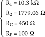
These are the values we have so far:
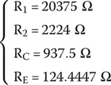
However, most of these values do not exist in the market. We must replace them with the available values listed on Appendix G.
The next list contains the values we have chosen for 20% tolerance resistors:
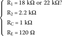
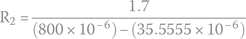
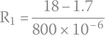
The calculated value for R1 = 20375 Ω is approximately equidistant of the available values of 18 and 22 kΩ. For this reason, we are not exactly sure which one we must choose.
To know which one is the best one for our purposes, let us test both options using a software simulator.2
The results provided by the simulator were the following:
Choosing R1 equal to 18 kΩ will increase the current across R1 from 800 μA to about 900 μA and an increase on the current across R2 from 764 μA to around 852 μA. These two changes modify the base voltage from 1.69 to 1.87 V.
Collector voltage drops from 9.81 to 7.52 V and the emitter voltage rises from 1.08 to 1.3 V. In technical terms, the output swing is now limited to vary from 3.3 to 18 V. This is not the middle point between 3.3 and 18 V.
If the collector voltage is now sitting at 7.52 V, it means that it can vary 10.48 V up, from 7.52 to 18 V, and just 4.22 V down, from 7.52 to 3.3 V. Because the output amplification must always be equally up and down, we must limit the amplification to swing 4.22 V up and down. So, the maximum output voltage we may have without clipping is a wave with 8.44 V peak to peak.
However, if we choose R1 to be 22 kΩ, the simulator tells us that the current across R1 will drop from 800 to 746 μA and the current across R2 will drop from 764 to 714 μA. These changes will modify the base voltage from 1.7 to 1.57 V.
The collector voltage will rise from 9.81 to 10.01 V, and the emitter voltage will drop from
 to
to  .
.The reader can already realize the changes now are less dramatic, compared with what we have designed.
The collector voltage sitting at 10.01 V provides output variations of 8 V up to 18 V and 7.049 V down to 2.961 V.
For the same reasons as before, the output must be limited to 7.049 V up and down, making the total output’s peak‐to‐peak amplitude equal to 14.098 V, almost twice the previous case.
Therefore, choosing R1 equal to 22 kΩ makes a much better amplifier, closer to what we have designed.
Notes
- 1 The reader will understand why this word is between quotes later in this book.
- 2 www.systemvision.com, for example, or any other the reader prefers.