30
Operational Amplifiers: A Brief Introduction
30.1 Introduction
In this chapter, we will do a brief explanation about operational amplifiers.
30.2 Operational Amplifiers
An operational amplifier or an op‐amp is a high‐gain voltage amplifier with a differential input and, generally, a single output. In this configuration, an op‐amp produces an output voltage that is commonly hundreds of thousands of times larger than the difference voltage between its input terminals.
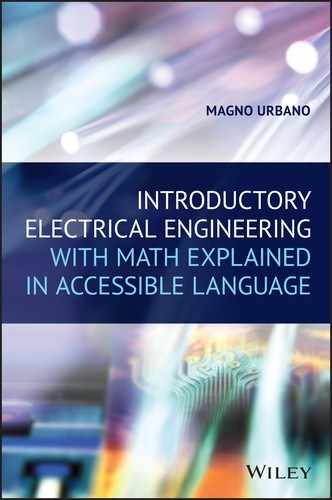
Figure 30.1 shows the symbol for the operational amplifier.
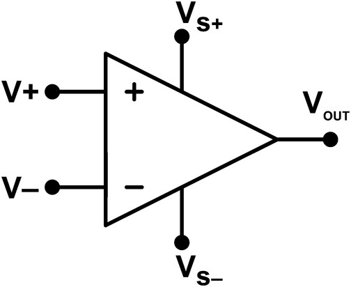
Figure 30.1 Operational amplifier.
30.3 How Op‐Amp Works
An op‐amp is basically a voltage amplifier to be used with external feedback components like resistors and capacitors between its inputs and output terminals. These components will determine the operation to be performed by the amplifier, for example, sum, subtraction, integration, differentiation, etc., which is the reason why it is called operational amplifier.
Op‐amps have two inputs, a non‐inverting input and an inverting input. These inputs are called differential inputs.
Internally they are as shown in Figure 30.2.

Figure 30.2 Operational amplifier (internal circuit).
Signals applied to the non‐inverting input will appear at the output amplified but with the same phase as the input, like shown in Figure 30.3.

Figure 30.3 Non‐inverting input.
However, if the same signal is applied to the inverting input, it will appear 180° inverted in phase at the output, as shown in Figure 30.4.
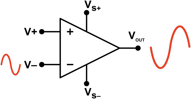
Figure 30.4 Inverting input.
As mentioned earlier, op‐amps have differential inputs, meaning that if the same signal is applied at both of its inputs, the output will be the difference, or the subtraction of both signals, as shown in Figure 30.5.
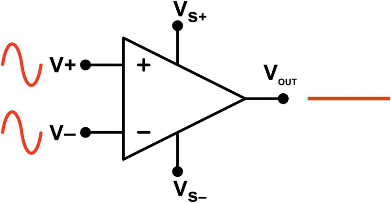
Figure 30.5 Differential inputs.
In Figure 30.5, the line at the output can be interpreted as 0 or as no change, meaning that the output will be constant if both inputs are the same. This is known as “common mode rejection ratio.”
VS+ and VS− terminals should be connected to the positive and negative power rails. Op‐amps generally like to operate with symmetrical power supplies, meaning that the power supply should provide a positive voltage, a negative voltage, and a ground reference.
If the reader remembers the mountain analogy, negative and positive voltages are relative and, therefore, can be simulated by, for example, establishing a voltage divider using two resistors, like shown in Figure 30.6.
Figure 30.5 shows two resistors in series connected to a 9‐V battery to create a voltage divider and simulate a symmetrical power supply with +4.5 V, −4.5 V, and ground (GND) in a configuration known as virtual ground. This method is very limited, and any current gain above certain levels will make the ground level to change, unbalancing the voltages.
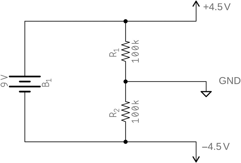
Figure 30.6 Virtual ground.
30.4 Op‐Amp Characteristics
- The voltage gain is very high, something that can go up to 10000 or more.
- Very high input impedance, generally near infinity, resulting in basically no current flowing into either of its two inputs and zero offset between the same inputs.
- Very low output impedance, generally near 0.
- The output of an op‐amp will be the difference between the voltage signals applied to its inputs multiplied by a certain gain.
- The gain of an op‐amp will be infinite if there is no element connecting the input and the output. In this case, the gain is known as “open‐loop gain.”
- If an element, like a resistor, is connected between the input and the output, the total gain will be reduced and therefore can be adjusted to a predetermined level.
30.5 Typical Configurations
An op‐amp can be basically configured as an inverting op‐amp and a non‐inverting op‐amp.
30.5.1 Inverting Op‐Amp
Figure 30.7 shows a typical inverting op‐amp circuit.
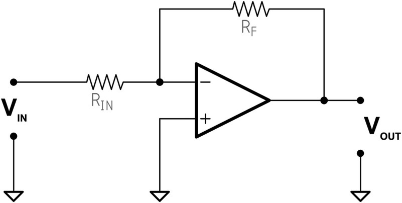
Figure 30.7 Inverting op‐amp.
To find the output voltage and consequently the gain, let us establish some points and currents, as shown in Figure 30.8.

Figure 30.8 Inverting amplifier (currents).
By using Kirchhoff’s current law, we know that
and that the current flowing across an op‐amp input is extremely low, is negligible, and can be considered 0.
Therefore,
We get the feedback current by applying nodal analysis to the output node:
The same nodal analysis can be applied to node X to get iIN:
We can substitute both equations in (30.1) and obtain
We know that the difference between the op‐amps inputs is 0, and we notice that the non‐inverting input is connected to ground. Therefore, the voltage across the non‐inverting input is 0, and consequently the voltage of the inverting input will also be 0, or
Substituting this in (30.2),
We get the final output voltage.
Consequently, the gain is
30.5.2 Non‐inverting Op‐Amp
Figure 30.9 shows a typical non‐inverting op‐amp circuit.

Figure 30.9 Non‐inverting op‐amp.
This kind of amplifier will amplify the signal and keep the signal with the same phase as the input.
To find the output voltage and consequently the gain, let us establish some points and currents, as shown in Figure 30.10.
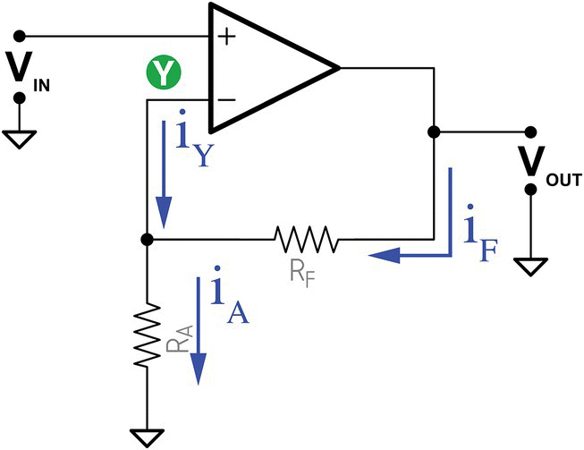
Figure 30.10 Non‐inverting amplifier (currents).
By applying Kirchhoff’s current law in node Y, we get
Like in the last example, we know that the current flowing across an op‐amp input is extremely low, is negligible, and can be considered 0.
Therefore,
We get the feedback current by applying nodal analysis to the output node:
The same nodal analysis can be applied to node Y to get iA:
We can substitute both equations in (30.3):


But we know that for op‐amps the input voltages are the same; therefore,
Consequently, we get the final formula for the output voltage,
and for the gain,
30.5.3 Voltage Follower
Figure 30.11 shows an amplifier where the feedback resistor, RF, was replaced with a wire.
This kind of configuration is called “voltage follower” or “buffer,” also known as “unity‐gain amplifier” or “isolation amplifier,” because this amplifier has a gain of 1, as follows:

Figure 30.11 Voltage follower.
But
therefore,
A voltage follower does not provide any amplification to the signal. The reason it is called a voltage follower is because the output voltage directly follows the input voltage, meaning the output voltage is the same as the input voltage. A voltage follower acts as an isolation, a buffer, providing no amplification or attenuation to the signal and can be used, for example, as an interface to interconnect two circuits, providing isolation between the two.
One example of the advantage of having isolation can be explained using the voltage divider circuit we have mentioned in Figure 30.6.
As explained earlier, this virtual ground works by the principle that the 9 V provided by the battery will be split into +4.5 V, −4.5 V, and ground. This will only work and keep the symmetry if the ground value remains stable at 0 V.
The big problem of this circuit is that the negative and the positive part of the power supply must supply circuits that drain the same current from both sides. If this is not true, the virtual ground will move from zero and the power supply will not be symmetrical anymore.
Let us see what happens if we connect a load of 10 kΩ to the negative part, as shown in Figure 30.12.

Figure 30.12 Virtual ground plus load.
Resistors R2 and RL are now in parallel. According to the first Ohm law, they can be replaced by an equivalent:
The voltage divider will now be equal to what is shown in Figure 30.13.

Figure 30.13 Voltage divider as virtual ground.
The voltage divider that was composed of two 100 kΩ resistors is now composed of a resistor R1 of 100 kΩ and another resistor, REQ, of approximately 9 kΩ. This means that the voltage between ground and V− that was −4.5 V before is now just −0.75 V or six times less.
If the voltage dropped in the negative part, it raised on the positive side. Now the voltage between ground and V+ that was +4.5 V is now +8.25 V.
The conclusion is that the ground voltage is not in the middle between V− and V+, anymore.
Thus, a voltage divider using resistors is not a good solution to build a symmetrical power supply from a nonsymmetrical voltage source. We need something that can isolate the load from the divider. Any ideas how we can accomplish this?
The solution to our problem is the one shown in Figure 30.14.

Figure 30.14 Voltage divider improved with a voltage follower.
Now, the voltage follower input is connected between the load RL and the voltage divider, isolating one from the other. The current drained by the load will not affect the voltage divider that much and will keep its value stable. This solution is not completely perfect but is better than having the voltage divider alone.
This solution works because the op‐amp offers a very high input impedance and, for that reason, will drain very little current from the voltage divider. With a very high input impedance, something around 100 MΩ or more, it is now that impedance in parallel with R2 that gives an equivalent resistor still equal to R2, keeping the relationship between R1 and R2 the same and consequently the voltage balance stable.
The following are simple examples of circuits using op‐amps.
30.5.4 Non‐inverting Summing Amplifier
Figure 30.15 shows a non‐inverting summing amplifier that can be used to add multiple voltages.

Figure 30.15 Non‐inverting summing amplifier.
To find the output voltage, let us establish some points and currents, as shown in Figure 30.16.
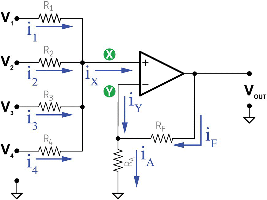
Figure 30.16 Non‐inverting summing amplifier (currents).
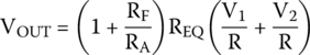
We have already calculated previously in this chapter that the output voltage for the non‐inverting amplifier is
or in this given example,
We know that both op‐amps have the same voltage, or
Therefore, the following formula is also true:
We also know that the sum of the input currents is equal to the current flowing into the non‐inverting input, or
However, the current flowing across an op‐amp input is extremely low and negligible, and we can consider it to be 0.
Therefore,
We get each current by applying nodal analysis to node X, for each input.
Therefore,
and so on for the multiple inputs.
By substituting these equations into (30.5), we obtain
We can expand this equation into
Isolating all VX on one side,
We notice that the block
is equal to the equivalent resistance of resistors in parallel and we can, consequently, replace the whole block with that resistance, or
Therefore, by substituting this into (30.6), we get
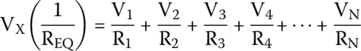
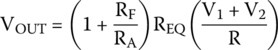
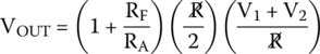
Upon substituting (30.7) in (30.4), we get the final equation for the output voltage.
30.5.4.1 Summing Two Inputs
If we are summing just two signals and the input resistors are the same, a very typical case in the real world, the output voltage will be
We know that the equivalent resistor of two resistors in parallel is
For two equal resistors, we have
By substituting into (30.9), we get the final formula for the output voltage for two inputs,

30.5.4.2 Summing Three Inputs
If we have three inputs, the result is slightly different.
We know that the equivalent resistor of three resistors in parallel is
If we solve that for equal resistors, we have
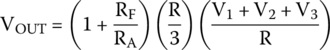
By substituting into (30.10), we get the final formula for the output voltage for three inputs,
30.5.5 Inverting Summing Amplifier
This case is like the previous one, where we want to sum several input signals. However, this is an inverter amplifier, where the output is 180° out of phase, compared to the input.
To sum more than two voltages, the inverting summing amplifier circuit, as shown in Figure 30.17, is the best one to choose.

Figure 30.17 Inverting summing amplifier.
To find the output voltage, let us establish some points and currents, as shown in Figure 30.18.

Figure 30.18 Inverting summing amplifier (currents).
We have already calculated previously in this chapter that the output voltage for the inverting amplifier is
or in this given example,
We know that both inputs have the same voltage. Because the non‐inverting input is connected to ground, we have
We know that the sum of the input currents is equal to the current flowing into the inverting input, or
However, the current flowing across an op‐amp input is extremely low and negligible, and we can consider it to be 0.
Therefore,
We get each current by applying nodal analysis to node X, for each input.
Therefore,
and so on for the multiple inputs.
By substituting (30.12) into these equations, we get
Therefore, Equation (30.13) is now

and we get the final equation for the output voltage.
30.5.6 Integrator
Like explained at the beginning of this chapter, operational amplifiers have this name because they can perform mathematical operations. Performing the integral of the input signal is just one of these operations.
The output of this circuit is the integral of the input (see Figure 30.19).

Figure 30.19 Op‐amp integrator.
To find the output voltage equation, we start by specifying some currents and points, like shown in Figure 30.20.
By applying Kirchhoff’s current law to node X, we get
However, we know that the current flowing across any of the op‐amp inputs is negligible and can be considered to be 0.

Figure 30.20 Op‐amp integrator (currents).
Therefore,
By applying nodal analysis to node X, we find the current across R:
We know that both op‐amp inputs have the same voltage, which in this case is 0, because the non‐inverting input is connected to ground.
Thus,
and consequently,
For the capacitor case, we know that the current flowing across this element is
The voltage across the capacitor is
Therefore, the current is
By substituting
we get
We can substitute iRand iF in (30.14):
or,
If we integrate both sides, we get the formula for the voltage output.
30.5.7 Differentiator
The differentiator circuit, able to differentiate the input signal, is shown in Figure 30.21.

Figure 30.21 Differentiator.
To get the output voltage equation, we do the same thing we did in the previous example to get
where
Therefore,
We get the output voltage equation as follows.