14
Diodes and Transistors: Active Components
14.1 Introduction
In this chapter, we will examine diodes and transistors, the first two practical applications coming from the invention of N‐type and P‐type materials.
14.2 Diodes
We have explained before that PN junctions allow current to flow in one direction but not on the other. This is the exact definition of a diode.
When a diode is forward biased, current flows and behaves, roughly, like a closed switch or like a resistor of small value.
However, if reverse biased, a diode will block current flow and behave like an open switch or a resistor of large value.
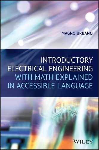
Figure 14.1 shows the symbol used for diodes. The triangle is the anode and the line represents the cathode, equivalent to materials P and N, respectively. The anode is the positive side and the cathode is the negative side.

Figure 14.1 Diode symbol.
14.3 NPN Junction
Suppose we add one more N‐type block to the PN structure and create an NPN block like shown in Figure 14.2. What happens now?

Figure 14.2 NPN structure.
Now, we have two electrical barriers between the two N‐type and the P‐type materials.
If the junction PN is equal to a diode, this NPN block is equal to two connected diodes like shown in Figure 14.3.
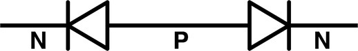
Figure 14.3 NPN junction “diodes.”
14.4 Biasing
Suppose that we take our NPN junction and connect it to a battery, like shown in Figure 14.4.
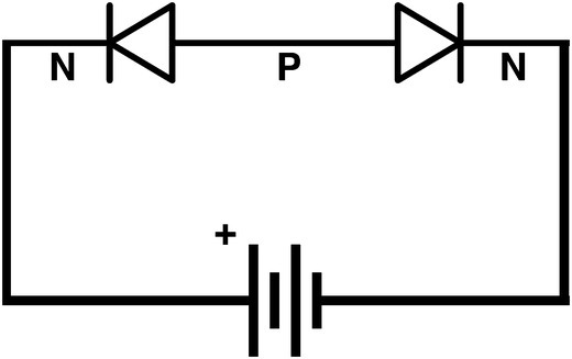
Figure 14.4 NPN structure and a battery.
If the battery can provide a voltage superior to 0.7 V, it will make the first N‐type element more positive and the second N‐type element more negative than normal. This will make the diodes be polarized as illustrated in Figure 14.5.

Figure 14.5 NPN structure and a battery.
The cathode of the first diode is now positive and its anode is negative, meaning that it is reverse biased and will not conduct current. However, the second diode has its anode positive and its cathode negative, meaning it is forward biased and can conduct current.
If we reverse the battery, the first diode will be forward biased and the second one reverse biased.
14.5 The Transistor, Finally!
The NPN structure we have already shown in Figure 14.3 is, in fact, what we call NPN transistor. Its symbol is shown in Figure 14.6.
Figure 14.6 NPN transistor.
In Figure 14.6, we see that transistors are formed by three parts, called collector (C), base (B), and emitter (E). The collector and the emitter are the N‐type materials and the base is the P‐type material. The base is the point where both elements connect.
There is another kind of transistor called PNP transistor. We will not talk about PNP transistors in this book because they work similarly to the NPN equivalents. The only difference is that current flows in the opposite directions and their voltages are reversed. Figure 14.7 shows their symbol.
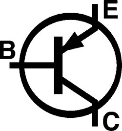
Figure 14.7 PNP transistor.
14.5.1 How Transistors Work?
We will examine in detail how transistors work late in this book, but broadly speaking, a transistor is a device that lets current flow from collector to emitter controlled by the current that flows into its base. The larger the current flowing into the base, the larger the current flowing from collector to emitter.1
Current will flow from collector to emitter only if the base voltage is, at least, 0.7 V greater than the emitter voltage.
When a transistor conducts, or enters the “on” state, the collector–emitter junction is seen, by the circuit, as a resistor of a small value.
When a transistor cuts off, or enters the “off” state, that is, does not conduct, the collector–emitter junction is seen as an open circuit.
The amount of current flowing into the base will control the amount of current flowing from collector to emitter. A small base current will make a huge current flow from collector to emitter.
How huge a collector current is compared with the base current is called current gain, known as hFE2 or β (beta). Values like 10, 20, 60, 300, 600, or more for hFE are common, depending on the transistor.
Figure 14.8 shows a general‐purpose low power transistor in a TO‐92 package.

Figure 14.8 Low power transistor (TO‐92 package).