2.5 TI C55x DSP
The Texas Instruments C55x DSP is a family of digital signal processors designed for relatively high performance signal processing. The family extends on previous generations of TI DSPs; the architecture is also defined to allow several different implementations that comply with the instruction set.
Accumulator architecture
The C55x, like many DSPs, is an accumulator architecture, meaning that many arithmetic operations are of the form accumulator = operand + accumulator. Because one of the operands is the accumulator, it need not be specified in the instruction. Accumulator-oriented instructions are also well-suited to the types of operations performed in digital signal processing, such as a1 x1 + a2 x2 + …. Of course, the C55x has more than one register and not all instructions adhere to the accumulator-oriented format. But we will see that arithmetic and logical operations take a very different form in the C55x than they do in the ARM.
Assembly language format
C55x assembly language programs follow the typical format:
MPY *AR0, *CDP+, AC0
label: MOV #1, T0
Assembler mnemonics are case-insensitive. Instruction mnemonics are formed by combining a root with prefixes and/or suffixes. For example, the A prefix denotes an operation performed in addressing mode while the 40 suffix denotes an arithmetic operation performed in 40-bit resolution. We will discuss the prefixes and suffixes in more detail when we describe the instructions.
The C55x also allows operations to be specified in an algebraic form:
AC1 = AR0 * coef(*CDP)
2.5.1 Processor and Memory Organization
We will use the term register to mean any type of register in the programmer model and the term accumulator to mean a register used primarily in the accumulator style.
Data types
The C55x supports several data types:
Registers
The C55x has a number of registers. Few to none of these registers are general-purpose registers like those of the ARM. Registers are generally used for specialized purposes. Because the C55x registers are less regular, we will discuss them by how they may be used rather than simply listing them.
Most registers are memory-mapped—that is, the register has an address in the memory space. A memory-mapped register can be referred to in assembly language in two different ways: either by referring to its mnemonic name or through its address.
Program counter and control flow
The program counter is PC. The program counter extension register XPC extends the range of the program counter. The return address register RETA is used for subroutines.
Accumulators
The C55x has four 40-bit accumulators AC0, AC1, AC2, and AC3. The low-order bits 0-15 are referred to as AC0L, AC1L, AC2L, and AC3L; the high-order bits 16-31 are referred to as AC0H, AC1H, AC2H, and AC3H; and the guard bits 32-39 are referred to as AC0G, AC1G, AC2G, and AC3G. (Guard bits are used in numerical algorithms like signal processing to provide a larger dynamic range for intermediate calculations.)
Status registers
The architecture provides six status registers. Three of the status registers, ST0 and ST1 and the processor mode status register PMST, are inherited from the C54x architecture. The C55x adds four registers ST0_55, ST1_55, ST2_55, and ST3_55. These registers provide arithmetic and bit manipulation flags, a data page pointer and auxiliary register pointer, and processor mode bits, among other features.
Stack pointers
The stack pointer SP keeps track of the system stack. A separate system stack is maintained through the SSP register. The SPH register is an extended data page pointer for both SP and SSP.
Auxiliary and coefficient data pointer registers
Eight auxiliary registers AR0-AR7 are used by several types of instructions, notably for circular buffer operations. The coefficient data pointer CDP is used to read coefficients for polynomial evaluation instructions; CDPH is the main data page pointer for the CDP.
Circular buffers
The circular buffer size register BK47 is used for circular buffer operations for the auxiliary registers AR4-7. Four registers define the start of circular buffers: BSA01 for auxiliary registers AR0 and AR1; BSA23 for AR2 and AR3; BSA45 for AR4 and AR5; and BSA67 for AR6 and AR7. The circular buffer size register BK03 is used to address circular buffers that are commonly used in signal processing. BKC is the circular buffer size register for CDP. BSAC is the circular buffer coefficient start address register.
Single repeat registers
Repeats of single instructions are controlled by the single repeat register CSR. This counter is the primary interface to the program. It is loaded with the required number of iterations. When the repeat starts, the value in CSR is copied into the repeat counter RPTC, which maintains the counts for the current repeat and is decremented during each iteration.
Block repeat registers
Several registers are used for block repeats—instructions that are executed several times in a row. The block repeat counter BRC0 counts block repeat iterations. The block repeat start and end registers RSA0L and REA0L keep track of the start and end points of the block.
The block repeat register 1 BRC1 and block repeat save register 1 BRS1 are used to repeat blocks of instructions. There are two repeat start address registers RSA0 and RSA1. Each is divided into low and high parts: RSA0L and RSA0H, for example.
Temporary registers
Four temporary registers T0, T1, T2, and T3 are used for various calculations. These temporary registers are intended for miscellaneous use in code, such as holding a multiplicand for a multiply, holding shift counts, and so on.
Transition registers
Two transition register TRN0 and TRN1 are used for compare-and-extract-extremum instructions. These instructions are used to implement the Viterbi algorithm.
Data and peripheral page pointers
Several registers are used for addressing modes. The memory data page start address registers DP and DPH are used as the base address for data accesses. Similarly, the peripheral data page start address register PDP is used as a base for I/O addresses.
Interrupts
Several registers control interrupts. The interrupt mask registers 0 and 1, named IER0 and IER1, determine what interrupts will be recognized. The interrupt flag registers 0 and 1, named IFR0 and IFR1, keep track of currently pending interrupts. Two other registers, DBIER0 and DBIER1, are used for debugging. Two registers, the interrupt vector register DSP (IVPD) and interrupt vector register host (IVPH), are used as the base address for the interrupt vector table.
The C55x registers are summarized in Figure 2.21.
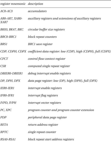
Figure 2.21 Registers in the TI C55x.
Memory map
The C55x supports a 24-bit address space, providing 16 MB of memory, as shown in Figure 2.22. Data, program, and I/O accesses are all mapped to the same physical memory. But these three spaces are addressed in different ways. The program space is byte-addressable, so an instruction reference is 24 bits long. Data space is word-addressable, so a data address is 23 bits. (Its least-significant bit is set to 0.) The data space is also divided into 128 pages of 64K words each. The I/O space is 64K words wide, so an I/O address is 16 bits. The situation is summarized in Figure 2.23.
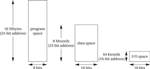
Figure 2.22 Address spaces in the TMS320C55x.
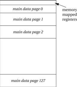
Figure 2.23 The C55x memory map.
Not all implementations of the C55x may provide all 16 MB of memory on chip. The C5510, for example, provides 352 KB of on-chip memory. The remainder of the memory space is provided by separate memory chips connected to the DSP.
The first 96 words of data page 0 are reserved for the memory-mapped registers. Because the program space is byte-addressable, unlike the word-addressable data space, the first 192 words of the program space are reserved for those same registers.
2.5.2 Addressing Modes
Addressing modes
The C55x has three addressing modes:
• Absolute addressing supplies an address in the instruction.
Absolute addressing
Absolute addresses may be any of three different types:
• A k16 absolute address is a 16-bit value that is combined with the DPH register to form a 23-bit address.
• A k23 absolute address is a 23-bit unsigned number that provides a full data address.
• An I/O absolute address is of the form port(#1234), where the argument to port() is a 16-bit unsigned value that provides the address in the I/O space.
Direct addressing
Direct addresses may be any of four different types:
Doffset is calculated by the assembler; its value depends on whether you are accessing a data page value or a memory-mapped register.
Soffset is an offset supplied by the programmer.
• Register-bit direct addressing accesses bits in registers. The argument @bitoffset is an offset from the least-significant bit of the register. Only a few instructions (register test, set, clear, complement) support this mode.
• PDP addressing is used to access I/O pages. The 16-bit address is calculated as
![]()
The PDPoffset identifies the word within the I/O page. This addressing mode is specified with the port() qualifier.
Indirect addressing
Indirect addresses may be any of four different types:
• AR indirect addressing uses an auxiliary register to point to data. This addressing mode is further subdivided into accesses into data, register bits, and I/O. To access a data page, the AR supplies the bottom 16 bits of the address and the top 7 bits are supplied by the top bits of the XAR register. For register bits, the AR supplies a bit number. (As with register-bit direct addressing, this only works on the register bit instructions.) When accessing the I/O space, the AR supplies a 16-bit I/O address. This mode may update the value of the AR register. Updates are specified by modifiers to the register identifier, such as adding + after the register name. Furthermore, the types of modifications allowed depend upon the ARMS bit of status register ST2_55: 0 for DSP mode, 1 for control mode. A large number of such updates are possible: examples include *ARn+, which adds 1 to the register for a 16-bit operation and 2 to the register for a 32-bit operation; *(ARn + AR0) writes the value of ARn + AR0 into ARn.
• Dual AR indirect addressing allows two simultaneous data accesses, either for an instruction that requires two accesses or for executing two instructions in parallel. Depending on the modifiers to the register ID, the register value may be updated.
• CDP indirect addressing uses the CDP register to access coefficients that may be in data space, register bits, or I/O space. In the case of data space accesses, the top 7 bits of the address come from CDPH and the bottom 16 come from the CDP. For register bits, the CDP provides a bit number. For I/O space accesses specified with port(), the CDP gives a 16 bit I/O address. Depending on the modifiers to the register ID, the CDP register value may be updated.
• Coefficient indirect addressing is similar to CDP indirect mode, but is used primarily for instructions that require three memory operands per cycle.
Any of the indirect addressing modes may use circular addressing, which is handy for many DSP operations. Circular addressing is specified with the ARnLC bit in status register ST2_55. For example, if bit AR0LC=1, then the main data page is supplied by AR0H, the buffer start register is BSA01, and the buffer size register is BK03.
Stack operations
The C55x supports two stacks: one for data and one for the system. Each stack is addressed by a 16-bit address. These two stacks can be relocated to different spots in the memory map by specifying a page using the high register: SP and SPH form XSP, the extended data stack; SSP and SPH form XSSP, the extended system stack. Note that both SP and SSP share the same page register SPH. XSP and XSSP hold 23-bit addresses that correspond to data locations.
The C55x supports three different stack configurations. These configurations depend on how the data and system stacks relate and how subroutine returns are implemented.
• In a dual 16-bit stack with fast return configuration, the data and system stacks are independent. A push or pop on the data stack does not affect the system stack. The RETA and CFCT registers are used to implement fast subroutine returns.
• In a dual 16-bit stack with slow return configuration, the data and system stacks are independent. However, RETA and CFCT are not used for slow subroutine returns; instead, the return address and loop context are stored on the stack.
• In a 32-bit stack with slow return configuration, SP and SSP are both modified by the same amount on any stack operation.
2.5.3 Data Operations
Move instruction
The MOV instruction moves data between registers and memory:
MOV src,dst
A number of variations of MOV are possible. The instruction can be used to move from memory into a register, from a register to memory, between registers, or from one memory location to another.
The ADD instruction adds a source and destination together and stores the result in the destination:
ADD src,dst
This instruction produces dst = dst + src. The destination may be an accumulator or another type. Variants allow constants to be added to the destination. Other variants allow the source to be a memory location. The addition may also be performed on two accumulators, one of which has been shifted by a constant number of bits. Other variations are also defined.
A dual addition performs two adds in parallel:
ADD dual(Lmem),ACx,ACy
This instruction performs HI(ACy) = HI(Lmem) + HI(ACx) and LO(ACy) = LO(Lmem) + LO(ACx). The operation is performed in 40-bit mode, but the lower 16 and upper 24 bits of the result are separated.
Multiply instructions
The MPY instruction performs an integer multiplication:
MPY src,dst
Multiplications are performed on 16-bit values. Multiplication may be performed on accumulators, temporary registers, constants, or memory locations. The memory locations may be addressed either directly or using the coefficient addressing mode.
A multiply and accumulate is performed by the MAC instruction. It takes the same basic types of operands as does MPY. In the form
MAC ACx,Tx,ACy
the instruction performs ACy = ACy + (ACx * Tx).
Compare instruction
The compare instruction compares two values and sets a test control flag:
CMP Smem == val, TC1
The memory location is compared to a constant value. TC1 is set if the two are equal and cleared if they are not equal.
The compare instruction can also be used to compare registers:
CMP src RELOP dst, TC1
The two registers can be compared using a variety of relational operators RELOP. If the U suffix is used on the instruction, the comparison is performed unsigned.
2.5.4 Flow of Control
Branches
The B instruction is an unconditional branch. The branch target may be defined by the low 24 bits of an accumulator
B ACx
or by an address label
B label
The BCC instruction is a conditional branch:
BCC label, cond
The condition code determines the condition to be tested. Condition codes specify registers and the tests to be performed on them:
• Test the value of an accumulator: <0, <=0, >0, >=0, =0, !=0.
• Test the value of the accumulator overflow status bit.
• Test the value of an auxiliary register: <0, <=0, >0, >=0, =0, !=0.
• Test the value of a temporary register: <0, <=0, >0, >=0, =0, !=0.
• Test the control flags against 0 (condition prefixed by !) or against 1 (not prefixed by !) for combinations of AND, OR, and NOT.
Loops
The C55x allows an instruction or a block of instructions to be repeated. Repeats provide efficient implementation of loops. Repeats may also be nested to provide two levels of repeats.
A single-instruction repeat is controlled by two registers. The single repeat counter, RPTC, counts the number of additional executions of the instruction to be executed; if RPTC = N, then the instruction is executed a total of N + 1 times. A repeat with a computed number of iterations may be performed using the computed single-repeat register CSR. The desired number of operations is computed and stored in CSR; the value of CSR is then copied into RPTC at the beginning of the repeat.
Block repeats perform a repeat on a block of contiguous instructions. A level 0 block repeat is controlled by three registers: the block repeat counter 0, BRC0, holds the number of times after the initial execution to repeat the instruction; the block repeat start address register 0, RSA0, holds the address of the first instruction in the repeat block; the repeat end address register 0, REA0, holds the address of the last instruction in the repeat block. (Note that, as with a single instruction repeat, if BRCn’s value is N, then the instruction or block is executed N + 1 times.)
A level 1 block repeat uses BRC1, RSA1, and REA1. It also uses BRS1, the block repeat save register 1. Each time that the loop repeats, BRC1 is initialized with the value from BRS1. Before the block repeat starts, a load to BRC1 automatically copies the value to BRS1 to be sure that the right value is used for the inner loop executions.
Nonrepeatable instructions
A repeat cannot be applied to all instructions—some instructions cannot be repeated.
Subroutines
An unconditional subroutine call is performed by the CALL instruction:
CALL target
The target of the call may be a direct address or an address stored in an accumulator. Subroutines make use of the stack. A subroutine call stores two important registers: the return address and the loop context register. Both these values are pushed onto the stack.
A conditional subroutine call is coded as:
CALLCC adrs,cond
The address is a direct address; an accumulator value may not be used as the subroutine target. The conditional is as with other conditional instructions. As with the unconditional CALL, CALLCC stores the return address and loop context register on the stack.
The C55x provides two types of subroutine returns: fast-return and slow-return. These vary on where they store the return address and loop context. In a slow return, the return address and loop context are stored on the stack. In a fast return, these two values are stored in registers: the return address register and the control flow context register.
Interrupts
Interrupts use the basic subroutine call mechanism. They are processed in four phases:
1. The interrupt request is received.
2. The interrupt request is acknowledged.
3. Prepare for the interrupt service routine by finishing execution of the current instruction, storing registers, and retrieving the interrupt vector.
4. Processing the interrupt service routine, which concludes with a return-from-interrupt instruction.
The C55x supports 32 interrupt vectors. Interrupts may be prioritized into 27 levels. The highest-priority interrupt is a hardware and software reset.
Most of the interrupts may be masked using the interrupt flag registers IFR1 and IFR2. Interrupt vectors 2-23, the bus error interrupt, the data log interrupt, and the real-time operating system interrupt can all be masked.
2.5.5 C Coding Guidelines
Some coding guidelines for the C55x [Tex01] not only provide more efficient code but in some cases should be paid attention to in order to ensure that the generated code is correct.
As with all digital signal processing code, the C55x benefits from careful attention to the required sizes of variables. The C55x compiler uses some nonstandard lengths of data types: char, short, and int are all 16 bits, long is 32 bits, and long long is 40 bits. The C55x uses IEEE formats for float (32 bits) and double (64 bits). C code should not assume that int and long are the same types, that char is 8 bits long or that long is 64 bits. The int type should be used for fixed-point arithmetic, especially multiplications, and for loop counters.
The C55x compiler makes some important assumptions about operands of multiplications. This code generates a 32-bit result from the multiplication of two 16-bit operands:
long result = (long)(int)src1 * (long)(int)src2;
Although the operands were coerced to long, the compiler notes that each is 16 bits, so it uses a single-instruction multiplication.
The order of instructions in the compiled code depends in part on the C55x pipeline characteristics. The C compiler schedules code to minimize code conflicts and to take advantage of parallelism wherever possible. However, if the compiler cannot determine that a set of instructions are independent, it must assume that they are dependent and generate more restrictive, slower code. The restrict keyword can be used to tell the compiler that a given pointer is the only one in the scope that can point to a particular object. The -pm option allows the compiler to perform more global analysis and find more independent sets of instructions.
Example 2.8 shows a C implementation of an FIR filter on the C55x.
Example 2.8 FIR Filter on the C55x
Here is assembly code generated by the TI C55x C compiler for the FIR filter with manually generated comments:
MOV AR0, *SP(#1) ; set up the loop
MOV T0, *SP(#0)
MOV #0, *SP(#2)
MOV #0, *SP(#3)
MOV *SP(#2), AR1
|| MOV #8, AR2
CMP AR1 >= AR2, TC1
|| NOP ; avoids Silicon Exception CPU_24
BCC $C$L2,TC1
; loop body
$C$L1:
$C$DW$L$_main$2$B:
MOV SP, AR3 ; copy stack pointer into auxiliary registers for address computation
MOV SP, AR2
MOV AR1, T0
AMAR *+AR3(#12) ; set up operands
ADD *SP(#2), AR3, AR3
MOV *SP(#3), AC0 ; put f into auxiliary register
AMAR *+AR2(#4)
MACM *AR3, *AR2(T0), AC0, AC0 ; multiply and accumulate
MOV AC0, *SP(#3) ; save f on stack
ADD #1, *SP(#2) ; increment loop count
MOV *SP(#2), AR1
|| MOV #8, AR2
CMP AR1 < AR2, TC1
|| NOP ; avoids Silicon Exception CPU_24
BCC $C$L1,TC1
; return for next iteration