
Chapter 38. Modern Graphics Hardware
In computer design it is a truism that smaller means faster.
Richard Russell
38.1. Introduction
All modern personal computers include special-purpose hardware to accelerate rasterized 2D and 3D rendering. With the exception of the interface that connects the PC to the display, this hardware is, strictly speaking, unnecessary, because the rendering could be done on the PC’s general-purpose processor. In this chapter we consider why PCs include special-purpose rendering hardware, how that hardware is organized, how it is exposed to you, the graphics programmer, and how it efficiently accelerates 3D rendering and other algorithms.
The history of computing includes many examples of failed special-purpose computing hardware. Examples include language accelerators, such as Lisp machines [Moo85] and Java interpreters [O’G10], numeric accelerators, and even graphics accelerators, such as the Voxel Flinger [ST91]. Modern graphics processing units, whose complexity and transistor counts can exceed those of the general-purpose CPU, are a prominent exception to this rule. Four conditions have allowed special-purpose graphics processing units, which we will refer to as GPUs, to become and remain successful. These are performance differentiation, workload sufficiency, strong market demand, and the inertia of ubiquity.
• Performance differentiation: Special-purpose hardware can execute graphics algorithms far more quickly than a general-purpose CPU. The most important reason is parallelization: GPUs employ tens or hundreds [Ake93] of separate processors, all working simultaneously, to execute graphics algorithms. While it is difficult to parallelize general computations, graphics algorithms are easily partitioned into separate tasks, each of which can be executed independently. They are thus more amenable to parallel implementation.1 Historically, graphics parallelization employed separate processors for the different stages in the graphics pipeline described in Chapters 1 and 14. In addition to pipeline parallelism, contemporary GPUs also employ multiple processors at each pipeline stage. The trend is toward increased per-stage parallelism in pipelines of fewer sequential stages.
1. Indeed, graphics is sometimes referred to as embarrassingly parallel, because it offers so many opportunities for parallelism.
Parallelism and other factors that contribute to GPU performance differentiation are explored further in Section 38.4.
• Workload sufficiency: Graphics workloads are huge. Interactive applications such as games render scenes comprising millions of triangles producing images, each comprising one or two million pixels, and do so 60 times per second or more. Current interactive rendering quality requires thousands of floating-point operations per pixel, and even this demand continues to increase. Thus, workloads of contemporary interactive graphics applications cannot be sustained by a single general-purpose CPU, or even by a small cluster of such processors.
• Strong market demand: Technical computing applications, in fields such as engineering and medicine, sustained a moderate market in special-purpose graphics accelerators during the 1980s and early 1990s. During this period companies such as Apollo Computer and Silicon Graphics developed much of the technological foundation that modern GPUs employ [Ake93]. But GPUs became a standard component of PC architecture only when demand for the computer games they enabled increased dramatically in the late ’90s.
• Ubiquity: Just as in the software and networking businesses, there is an inertia that inhibits utilization of uncommon, special-purpose add-ins, and that encourages and rewards their utilization when they have become ubiquitous. Strong market demand was a necessary condition for personal-computer GPUs to achieve ubiquity, but ubiquity also required that GPUs be interchangeable from an infrastructure standpoint. Two graphics interfaces—OpenGL [SA04] and Direct3D [Bly06]—have achieved industry-wide acceptance. Using these interfaces application programmers can treat GPUs from different manufacturers, and with different development dates, as being equivalent in all respects except performance. The abstraction that Direct3D defines is considered further in Section 38.3.
GPUs based on the classic graphics pipeline, exemplified by the NVIDIA GeForce 9800 GTX considered in the next section, have achieved a stable position in the architecture of personal computers. They are therefore well worth studying and understanding. The situation may change, however, as it has for so many other special-purpose functional units.
Parallelism, in the form of multiple processors (a.k.a. cores) on a single CPU, has replaced increasing clock frequency as the engine of exponential CPU performance improvement. The number of cores on a CPU is expected to increase exponentially, just as clock frequency has in the past. The resultant parallelism may make general-purpose CPUs more performance-competitive with GPUs, thereby reducing the demand for special-purpose hardware.
Alternatively, the limitations of the classic-pipeline architecture discussed in this chapter may allow a contending architecture to overcome and replace current GPUs. Because GPUs have tended toward brute force algorithms, such as the z-buffer visible-surface algorithm described in Chapter 36, the workload argument is somewhat circular: GPUs amplify their own work requirements by implementing inefficient algorithms. Accelerated ray tracing is one candidate architecture to replace current GPUs.
Perhaps the most likely outcome is that GPU architecture will steadily evolve, as it has in the past decade, to accommodate new algorithms and architecture features.
The remainder of this chapter describes graphics architectures in part by using three exemplars: the OpenGL and Direct3D software architectures, and the NVIDIA GeForce 9800 GTX GPU, released in April 2008. While this GPU is already fading in popularity, the decisions that influenced its design will remain current for a long while.
This chapter defines many terms that you’ve already encountered earlier in the book. It does so for two reasons: First, the reader with some prior experience in graphics may profitably read this chapter first, even though it appears at the end of the book; second, some definitions in this chapter have been chosen to correspond to industry practice (so that, for instance, a “color” is an RGB triple rather than a percept in the human brain!), and we want to be certain that you understand exactly what’s being said.
38.2. NVIDIA GeForce 9800 GTX
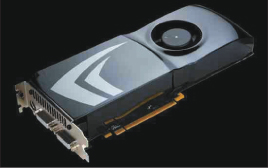
Figure 38.1 illustrates the key components and interconnections in a state-of-the-art personal computer (PC) system, as of early 2009. The Intel Core 2 Extreme QX9770 CPU, Intel X48 Express chipset, and NVIDIA GeForce 9800 GTX GPU were among the highest-performance components then available for desktop computing. This is the sort of system a serious computer gamer would have bought if the $5,000 price were within reach. With this context in mind, let’s look at the performance and design of the 9800 GTX GPU.

Like the Extreme CPU, the GTX GPU is a single component—a packaged silicon chip—that is mounted to a circuit board by hundreds of soldered circuit interconnections. The CPU, chipset, and CPU memory are mounted to the primary system circuit board, called the motherboard, along with most of the PC’s remaining electronics. The GPU and GPU memory are mounted to a separate PCIe circuit board that is connected to the motherboard through a multiconnector socket (see Figure 38.2).
Perhaps the most notable characteristic of the GeForce 9800 GTX is its extremely high performance. The GTX can render 340 million small triangles per second and, when rendering much larger triangles, a peak of almost 11 billion pixels per second. Executing application-specified code to compute the shaded colors of rendered pixels, the GTX can perform 576 billion floating-point operations per second (GFLOPS). This is more GFLOPS than the most powerful supercomputer available just over a decade ago, and is more than five times the 102.4 GFLOPS that the Intel Core 2 Extreme QX9770 CPU can sustain. Memory bandwidth—the rate data is moved between a processor chip and its external random access memory—is an equally important metric of performance. The Core 2 Extreme QX9770 CPU accesses external memory through the X48 Express chipset. While the chipset supports memory transfers at up to 25.6 GB/s, the Front Side Bus that connects the CPU to the chipset limits CPU-memory transfers to a maximum of 12.8 GB/s. The GPU accesses its memory directly and achieves a peak transfer rate of 70.4 GB/s, more than five times that available to the CPU.
In the same way that interest compounds on invested money, CPU and GPU performance have reached their current state through steady exponential increase. Underlying this exponential increase is Moore’s Law, Gordon Moore’s 1965 prediction that the number of transistors on an economically optimum integrated circuit would continue to increase exponentially, as it had since Intel had begun producing integrated circuits a few years earlier [Moo65]. Over the succeeding four decades the actual increase held steady at about 50% per year, resulting in the near-iconic status of Moore’s prediction. Compounding at high rates quickly results in huge gains. A decade of 50% annual compounding, for example, yields an increase of 1.510 = 57.67 times. And a decade of 100% annual compounding yields an increase of 210 = 1,024 times, so quantities with the same initial value that grow at these two rates differ by a factor of almost 20 after a decade. Driven by Moore’s Law, the storage capacity of integrated circuit memory, which is proportional to transistor count, has increased by a factor greater than ten million since its first commercial availability in the early 1960s.
Increased transistor count allows increased circuit complexity, which engineers parlay into increased performance through techniques such as parallelism (performing multiple operations simultaneously) and caching (keeping frequently used data elements in small, high-speed memory near computational units). Increases in transistor count are driven primarily by the steady reduction in the dimensions of transistors and interconnections on silicon integrated circuits. (The interconnections on the Intel Core 2 Extreme QX9770 CPU have a drawn width of just 45 nm, 1/2,000th the width of a human hair, and about one-tenth the wavelength of blue light.) Smaller transistors change state more quickly, and shorter interconnections introduce less delay, so circuits can be run at higher speeds. Increases in transistor count and circuit speed compound, allowing the performance of well-engineered components to increase at rates approaching 100% per year.
GPU designers have made excellent use of increases in both transistor count and circuit speed. Over the ten years between 2001 and 2010 performance metrics of NVIDIA GPUs, such as triangles drawn per second and pixels drawn per second, have increased by 70% to 90% per year. Memory bandwidth has increased by only 50% per year. But data compression techniques, themselves enabled by increased circuit complexity, have allowed an increase in effective memory bandwidth of 80% per year, supporting the correspondingly large increases in drawing performance.
CPU designers have taken full advantage of increased circuit speed, but they have been less successful converting increased transistor count into performance. CPU performance has historically increased by 50% per year, an amazing achievement, but still significantly lower than the 70% to 90% annual increases in GPU performance. Today’s relative performance advantage of GPUs over CPUs is the direct result of compounding performance at unequal rates.
Shortly after the year 2000, CPUs reached a power dissipation somewhat over 100 watts, near the maximum that can be dissipated by a single component in a personal computer cabinet. Because circuit power is directly proportional to circuit speed, the annual 20% increase in CPU clock speed, which had been a major driver of CPU performance increases for two decades, dropped suddenly to essentially zero. This event has motivated CPU designers to incorporate more parallelism into their circuits, an approach that has been very successful for GPUs. The Intel Core 2 Extreme QX9770 CPU is a quad-core design, meaning that it contains four microprocessor cores in a single component package. Dual-core Intel CPUs were introduced in 2005, and quad-core designs are now available. Each core has four floating-point Arithmetic and Logic Units (ALUs), each ALU including an addition unit and a multiplication unit, for a total of 32 floating-point units in the Core 2 Extreme QX9770. By comparison, the NVIDIA GeForce 9800 GTX GPU has 16 cores, each with eight floating-point ALUs, and each ALU with two multiplication units and one addition unit, for a total of 384 floating-point units. While the CPU cores are clocked at roughly twice the rate of the GPU cores (3.2 GHz to 1.5 Ghz), the sheer number of floating-point units in the GPU gives it a greater than five-to-one GFLOPS advantage (576 to 102).
In summary, as of 2009 GPUs sustained significantly higher performance than CPUs because they were doing more calculations in parallel, and they did this by devoting a greater percentage of their silicon area to computation than do CPUs. As of 2013, there’s no sign of this trend slowing down. GPU parallelism is considered further in the following sections.
38.3. Architecture and Implementation
When you write code that uses a GPU for graphics, you do not directly manipulate the hardware circuits of the GPU. Instead, you code to an abstraction, which is implemented by a combination of the GPU hardware, GPU firmware (code that runs on the GPU), and a device driver (code that runs on the CPU). The firmware and the device driver are implemented and maintained by the GPU’s manufacturer, which is NVIDIA in the case of the GeForce 9800 GTX. They are as fundamental to the implementation of the abstraction as the GPU hardware itself.
The distinction between an abstraction and its implementation, and the value conferred by this distinction, are familiar concepts in software development. Information hiding was introduced by Parnas in 1972 [Par72]. Today C++ developers isolate implementation details behind interfaces constructed using abstract classes. Prior to the development of C++, C programmers were trained to use functions, header files, and isolated code files to achieve many of the benefits that C++ classes came to provide.
The importance of separating interface and implementation was identified even earlier by computer hardware developers. Gerrit Blaauw and Fred Brooks, who with Gene Amdahl and others brought computing into the modern age with the creation of the IBM System/360 in 1964 [ABB64], define the architecture of a system as “the system’s functional appearance to its immediate user, its conceptual structure and functional behavior as seen by one who programs in machine language” [BJ97]. They use the terms implementation and realization to refer to the logical organization and physical embodiment of a system. Careful distinction between architecture and implementation2 allowed the System/360 to be implemented as a family of computers, with differing implementations and realizations (and correspondingly different costs and performances), but a single interface exposed to programmers. Code written for one member of the family was guaranteed to run correctly on all other family members.
2. Modern usage of the term “architecture” sometimes includes implementation, but we will maintain the distinction carefully in this chapter.
By analogy, Direct3D, which was introduced in Chapter 16 and further discussed in Section 15.7, and OpenGL specify the architecture of modern GPUs. They enable code portability just as the System/360 architecture did. But the analogy runs deeper. Both GPU architectures and CPU architectures do the following.
• They allow for differences in configuration, which for CPUs includes memory size, disk storage capacity, and I/O peripherals, and for GPUs includes framebuffer size, texture memory capacity, and specific color codings available in each.
• They make no specification of absolute performance, allowing implementations to cover a wide gamut of cost and optimization.
• They tightly specify the semantics of all inputs, both valid and invalid, to further ensure code compatibility.
An important way that GPU and CPU architectures differ is in level: Direct3D and OpenGL are specified as libraries of function calls, which are compiled into application code, while CPUs are described by instruction set architectures, or ISAs, for which instructions are generated by a compiler. The relatively higher level of abstraction of GPU architecture has given GPU implementors more room to innovate, and it is probably a factor in the historically greater rate of GPU performance increase discussed in the previous section. Both Direct3D and OpenGL were carefully designed to allow highly parallel implementations, for example.
38.3.1. GPU Architecture
While both Direct3D and OpenGL specify their abstractions in exacting detail, as befits an architectural specification, here we do not completely define either interface. Instead, we develop a simplified pipeline model that matches both architectures at the chosen level of detail. Figure 38.3 is a block diagram of this architecture.
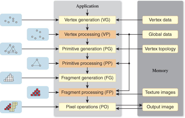
Figure 38.3: Graphics pipeline. This matches both Direct3D and OpenGL at this level of detail. Arrows indicate data flow while drawing.
As you’ve seen in earlier chapters, graphics architectures perform operations on aggregate data types—vertices, primitives (e.g., triangles), pixel fragments (often just fragments), and pixels—and on multidimensional arrays of pixels (e.g., 2D images and 1D, 2D, and 3D textures). Pixels in a texture are called texels. Operations are performed in the fixed sequence illustrated in Figure 38.3. The sequence cannot generally be modified by the application, although some stages (e.g., primitive processing) may be omitted.
We briefly review the operation of the graphics pipeline by considering the processing of a single triangle (see Figure 38.3, left column). Prompted by the application, the vertex generation stage creates three vertices from geometric and attribute data (e.g., coordinates and color) stored in memory. The vertices are passed to the vertex processing stage, where operations such as coordinate-space transformations are performed, resulting in homogeneous clip-coordinate vertices. The primitive generation stage assembles the clip-coordinate vertices into a single triangle, possibly accessing topology information in memory to do so. The triangle is passed to the primitive processing stage, where it may be culled, replaced by a finite set of related primitives (e.g., subdivided into four smaller triangles), or left unchanged. After reaching the fragment generation stage, the triangle is clipped against the viewing-frustum boundaries, projected to screen coordinates, then rasterized such that a fragment (a piece of geometry so small that it contributes to only a single pixel) is generated for each pixel in the output image that geometrically intersects the triangle. The fragment processing stage colors each fragment by performing lighting calculations and accessing texture images. Finally, the colored fragment is merged into the corresponding pixel in the output image. Operations performed in the pixel operation stage, such as z-comparisons and simple color arithmetic, determine whether and how the fragment values affect or replace corresponding pixel values.
Three of the pipeline stages—the vertex, primitive, and fragment processing stages—are application-programmable. A (typically) simple program, specified by the application using a C-like language, is assigned to the fragment processing stage, where it is executed on each fragment. Likewise, programs are specified and assigned to the vertex and primitive processing stages, where they operate on individual vertices and primitives. Floating-point arithmetic, logical operations, and conditional flow control are supported by each programmable processing stage, as are indexing of global data and filtered sampling (i.e., interpolation) of texture images, both stored in memory. The remaining stages—the vertex, primitive, and fragment generation stages and the pixel operations stage—are referred to as fixed-function stages, because they cannot be programmed by the application. (They can, however, be configured by various modal specifications.)
Modern graphics architectures support two types of commands, those that specify state (the majority) and those that cause rendering to occur. Thus, drawing is a two-step process: 1) Set up all the required state, and then 2) run the pipeline to cause drawing to happen.3 Vertex data and topology, texture images, and the application-specified programs for the processing stages are all large components of pipeline state. In addition, modal state associated with each fixed-function stage determines the details of its operation (e.g., aliased or antialiased rasterization at the fragment generation stage). Figure 38.3 emphasizes drawing, rather than state setup, both by omitting modal state and by indicating read-only access to bulk memory state (e.g., texture images).
3. Early OpenGL interfaces blurred this distinction by providing commands that both specified vertex state and resulted in drawing. This is what is usually meant by the term “immediate-mode” rendering, as discussed in Chapter 16.
Certain properties of the graphics pipeline architecture have great significance for both graphics applications and GPU implementations. One such property is read-only access, during drawing operation, of all bulk memory state other than the output image. (Writing greatly complicates coherence, the requirement that memory state values appear consistent to all the processors in a parallel system [see Section 38.7.2].) Perhaps even more significant is the requirement for in-order operation. This applies both to drawing (fragments must reach the output image in the order that their corresponding triangles were specified) and to state changes (drawing activated prior to a state change cannot be affected by that change, and drawing specified after must be). GPU implementors struggle mightily with in-order drawing, while read-only bulk state (state such as texture memory that cannot be modified during rendering operation) simplifies their task. Conversely, application developers are constrained by read-only state semantics, but they are supported by in-order drawing semantics. The art of architecture design includes identifying such conflicts and making the best tradeoffs. If either constituency is entirely happy with the architecture, it probably isn’t right. This is so important that we embody it in a principle.
![]() The Design Tradeoff Principle
The Design Tradeoff Principle
The art of architecture design includes identifying conflicts between the interests of implementors and users, and making the best tradeoffs.
38.3.2. GPU Implementation
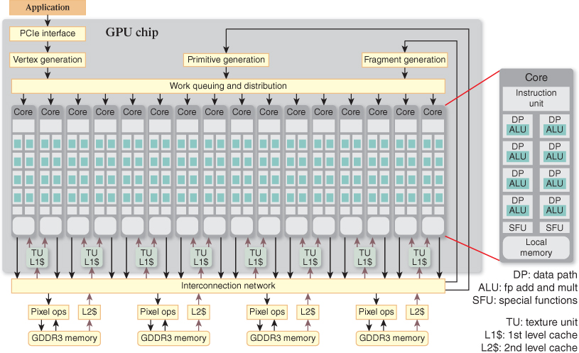
Now we turn our attention to an implementation of the graphics pipeline architecture—NVIDIA’s GeForce 9800 GTX. Figure 38.4 is a block-diagram depiction of this implementation. Block names have been chosen to best illustrate the correspondence to the blocks on the pipeline block diagram shown in Figure 38.3. There is a one-to-one correspondence between the vertex, primitive, and fragment generation stages in the pipeline and the identically named blocks in the implementation diagram. Conversely, all three programmable stages in the pipeline correspond to the aggregation of 16 cores, eight texture units (TUs), and the block titled “Work queuing and distribution.” This highly parallel, application-programmable complex of computing cores and fixed-function hardware is central to the GTX implementation—we’ll have much more to say about it. Completing the correspondence, the pixel operation stage of the pipeline corresponds to the four pixel ops blocks in the implementation diagram, and the large memory block adjacent to the pipeline corresponds to the aggregation of the eight L1$, four L2$, and four GDDR3 memory blocks in the implementation. The PCIe interface and interconnection network implementation blocks represent a significant mechanism that has no counterpart in the architectural diagram. A few other significant blocks, such as display refresh (regularly transferring pixels from the output image to the display monitor) and memory controller logic (a complex and highly optimized circuit), have been omitted from the implementation diagram.
38.4. Parallelism
As we have seen, several decades of exponential increase in transistor count and performance have given computer system designers ample resources to design and build high-performance systems. Fundamentally, computing involves performing operations on data. Parallelism, the organization and orchestration of simultaneous operation, is the key to achieving high-performance operation. It is the subject of this section. We defer the discussion of data-related performance to Section 38.6.
We are all familiar with doing more than one thing at the same time. For example, you may think about computer graphics architecture while driving your car or brushing your teeth. In computing we say that things are done in parallel if they are in process at the same time. In this chapter, we’ll further distinguish between true and virtual parallelism. True parallelism employs separate mechanisms in physically concurrent operation. Virtual parallelism employs a single mechanism that is switched rapidly from one sequential task to another, creating the appearance of concurrent operation.
Most parallelism that we are aware of when using a computer is virtual. For example, the motion of a cursor and of the scroll bar it is dragging appear concurrent, but each is computed separately on a single processing unit. By allowing computing resources to be shared, and indeed by allocating resources in proportion to requirements, virtual parallelism facilitates efficiency in computing. But it cannot scale performance beyond the peak that can be delivered by a single computing element.
All computing hardware therefore employs true parallelism to increase computing performance. For example, even a so-called scalar processor, which executes a single instruction at a time, is in fact highly parallel in its hardware implementation, employing separate specialized circuits concurrently for address translation, instruction decoding, arithmetic operation, program-counter advancement, and many other operations. At an even finer level of detail, both address translation and arithmetic operations utilize binary-addition circuits that employ per-bit full adders and “fast-carry” networks that all operate in parallel, allowing the result to be computed in the period of a single instruction. In a modern, high-performance integrated circuit the longest sequential path typically employs no more than 20 transistors, yet billions of transistors are employed overall. The circuit must be massively parallel.
Because true hardware parallelism is an implementation artifact, it cannot be specified architecturally. Instead, an architecture specifies parallelism that can be implemented either virtually (by sharing hardware circuits) or truly (with separate hardware circuits), or, typically, through a combination of the two. To better understand these alternatives, and to illustrate that parallelism has long been central to computing performance, we will briefly consider the architecture and implementation of a decades-old system: the CRAY-1 supercomputer.
The CRAY-1 was developed by Cray Research, Inc., primarily to satisfy the computing needs of the U.S. Department of Defense (see Figure 38.5). When introduced in 1976, it was the fastest scalar processor in the world: Its cycle time of 12.5 ns supported the execution of 80 million instructions per second.4 Key to its peak performance of 250 million floating-point operations per second (MFLOPS), however, were special instructions that specified arithmetic operations on vectors of up to 64 operands. Data vectors were gathered from memory, stored in 64-location vector registers, and operated on by arithmetic vector instructions (e.g., the vector sum or vector per-element product of two vector operands could be computed), and the results returned to main memory.
4. The analysis in this discussion is slightly simplified, because even in scalar operation the CRAY-1 could in some cases execute two instructions per cycle.
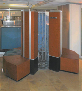
Figure 38.5: The CRAY-1 supercomputer was the fastest system available when it was introduced in 1976. (Courtesy of Clemens Pfeiffer. Original image at http://upload.wikimedia.org/wikipedia/commons/f/f7/Cray-1-deutschesmuseum.jpg.)
Because these per-element operations had no dependencies (i.e., the sum of any pair of vector elements is independent of the values and sums at all other pairs of vector elements) the 64 operations specified by a vector instruction could all be computed at the same time. While such an implementation was possible in principle, it was impractical given the circuit densities that could be achieved using the emitter-coupled transistor logic (ECL) that was employed. Indeed, had such an implementation been possible, its peak performance would have approached 64 × 80,000,000 = 5,120 MFLOPS, more than 20 times the peak performance that was actually achieved. Instead, the architectural parallelism of equivalent operations on 64 data pairs was implemented as virtual parallelism—the 64 operations were computed sequentially using a single arithmetic circuit.
The roughly 3x improvement in peak arithmetic performance over scalar performance was instead achieved using a parallelism technique called pipelining. Two specific circuit approaches were employed. First, because floating-point operations are too complex to be computed by a single ECL circuit in 12.5 ns, the floating-point circuits were divided into stages: 6 for addition, 7 for multiplication, and 14 for reciprocation. Each stage performed a portion of the operation in a single cycle, then forwarded the partial result to the next stage. Thus, floating-point operations were organized into pipelines of sequential stages (e.g., align operands, check for overflow), with the stages operating in parallel and the final stage of each unit producing a result each cycle. The reduced complexity of the individual stages allowed the 12.5 ns cycle time to be achieved, and therefore enabled sustained scalar performance of 80 MFLOPS. Second, a specialized pipelining mechanism called chaining allowed the results of one vector instruction to be used as input to a second vector instruction immediately, as they were computed, rather than waiting for the 64 operations of the first vector instruction to be completed. As illustrated in Figure 38.6, this allowed small compound operations on vectors, such as a × (b + c), to be computed in little more time than was required for a single vector operation. In the best case, with all three floating-point processors active, the combination of stage pipelining and operation chaining allows a performance of 250 MFLOPS to be sustained.
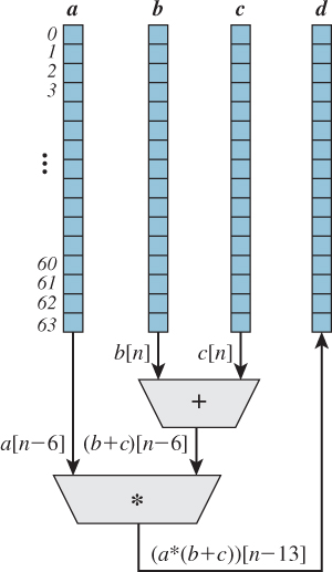
Figure 38.6: Chained evaluation of the vector expression d = a × (b + c) on the CRAY-1 supercomputer. The floating-point addition unit takes six pipelined steps to compute its result; the multiplication unit takes seven.
Another important characterization of parallelism is into task and data parallelism. Data parallelism is the special case of performing the same operation on equivalently structured, but distinct, data elements. The CRAY-1 vector instructions specify data-parallel operation: The same operation is performed on up to 64 floating-point operand pairs. Task parallelism is the general case of performing two or more distinct operations on individual data sets. Pipeline parallelism, such as the CRAY-1 floating-point circuit stages and operation chaining, is a specific organization of task parallelism. Other examples of task parallelism include multiple threads in a concurrent program, multiple processes running on an operating system, and, indeed, multiple operating systems running on a virtual machine.
GPU parallelism can also be characterized using these distinctions. GPU architecture (see Figure 38.3) is a task-parallel pipeline. The GeForce 9800 GTX implementation of this pipeline is a combination of true pipeline parallelism and virtual pipeline parallelism. Fixed-function vertex, primitive, and fragment generation stages are implemented with separate circuits—they are examples of true parallelism. Programmable vertex, primitive, and fragment processing stages are implemented with a single computation engine that is shared among these distinct tasks. Virtualization allows this expensive computation engine, which occupies a significant fraction of the GPU’s circuitry, to be allocated dynamically, based on the instantaneous requirements of the running application. A true-parallel implementation would assign fixed amounts of circuitry to these pipeline tasks, and thus would be efficient only for applications that tuned their vertex, primitive, and fragment workloads to the static, circuit-specified allocations. Such a static allocation is forced for the fixed-function stages, but these circuits occupy a small fraction of the overall GPU, so they can be overprovisioned without significantly increasing the cost of the GPU.
Task parallelism, in the form of pipeline stages, is only the top level of a hierarchy of parallelism in the GeForce 9800 GTX implementation, which continues down to small groups of transistors. The next lower layers of parallelism are the 16 task-parallel computing cores, each of which is implemented as a data-parallel, 16-wide vector processor. Unlike the CRAY-1, whose vector implementation was virtual parallel, the GeForce 9800 GTX vector implementation is a hybrid of virtual and true parallel—there is separate circuitry for eight vector data paths, each of which is used twice to operate on a 16-wide vector. (This parallel circuitry is represented by the eight data paths [DPs] in each of the 16 cores of Figure 38.4.) A true-parallel vector implementation is sometimes referred to as SIMD (Single Instruction Multiple Data) because a single decoded instruction is applied to each vector element. SIMD cores are desirable because they yield much more computation (GFLOPS) per unit area of silicon than scalar (SISD) cores do. And compute rate is a high priority for GPU implementations.
It is important to understand that SIMD vector implementation of the GPU cores is not revealed directly in the GPU architecture (as it is in the CRAY-1 vector instructions). While the GPU programming model executes the same program for each element (e.g., each vertex), that vertex program may contain branches, and the branches may be taken differently for each vertex. The implementation includes extra circuitry that implements predication. When all 16 vector data elements take the same branch path, operation continues at full efficiency. A single branch taken differently splits the vector data elements into two groups: those that take one branch path and those that take the other. Both paths are executed, one after the other, with execution suppressed for elements that don’t belong to the path being executed. (Figure 38.9 in Section 38.7.3 illustrates diverging and nondiverging predicated execution.) Nested branches may further split the groups. In the limit separate execution could be required for each element, but this limit is rarely reached. Thus, a Single Program Multiple Data (SPMD) architecture is implemented with predicated SIMD computation cores.
38.5. Programmability
We begin our discussion of programmability by examining a simple coding example. Listing 38.1 is a complete fragment processing program written in the Direct3D High-Level Shading Language (HLSL). This program specifies the operations that are applied to each pixel fragment5 resulting from the rasterization of a primitive. While more complex operations are often specified, in this case the operation is a simple one: The red, green, blue, and alpha components of the fragment’s color are attenuated by the floating-point variable brightness. The term shader, taken from Pixar’s RenderMan Shading Language, is often used to refer to fragment processing programs (and also to vertex processing and primitive processing programs) although they have far more functionality than simply computing color.
5. Use of the term “fragment” to distinguish the data structures generated by rasterization (and operated upon by the fragment processing pipeline stage) from the data structures stored in the framebuffer (pixels) was established by OpenGL in 1992 and has since become an accepted industry standard. Microsoft Direct3D and HLSL blur this distinction by referring to both data structures as pixels. The confusion is compounded by the HLSL use of “fragment” to refer to a separable piece of HLSL code. The reader is warned.
Listing 38.1: A simple HLSL fragment processing program (Microsoft refers to this as a “pixel shader”). Fragment color is attenuated by the floating-point variable brightness.
1 float brightness = 0.5;
2
3 struct v2f {
4 float4 Position : POSITION;
5 float4 Color : COLOR0;
6 };
7
8 struct f2p {
9 float Depth : DEPTH0;
10 float4 Color : COLOR0;
11 }
12
13 // attenuate fragment brightness
14 void main(in v2f Input, out f2p Output) {
15 Output.Depth = Input.Position.z;
16 Output.Color = brightness * Input.Color;
17 }
HLSL is designed to be familiar to C and C++ programmers. As it would in C++, the first line of the shader declares brightness as a global, floating-point variable with initial value 0.5. Again, as in C++, because brightness is a global variable, its value can be changed by nonlocal code. In HLSL such nonlocal code includes the code of the Direct3D application that is driving the GPU pipeline. For example, the application can change the value of brightness to 0.75 by calling the Direct3D function.
SetFloat("brightness",0.75);
Structures v2f and f2p are defined much as they would be in C++. There are two important additions: vector data types and semantics. Vector data types, such as float4, are a shorthand notation that is similar to a C++ array typedef (in this case, typedef float[4] float4;), but with additional capabilities. This notation can be used for vectors of lengths two, three, and four. It is also available for square matrices (e.g., float4x4) and for all HLSL data types (i.e., for half, float, double, int, and bool). Semantics are the predefined tokens, such as POSITION and COLOR0, that are separated by colons from the variable names (such as Position and Color). These tokens associate HLSL-program variables with mechanisms in the fixed-function stages of the pipeline—they are the glue that connects application-specified shaders to architecture-specified fixed-function mechanisms.
Operation of the fragment shader is specified by the main function. Input to main is through structure variable Input of type v2f, and output is through structure variable Output of type f2p. In the body of main the output depth value is copied from the input depth value, while the output color is set to the attenuated input color. Note that HLSL defines multiplication of a vector value (Input.Color) by a scalar value (brightness) in the mathematical sense: The result is a vector of the same dimension, with each component multiplied by the scalar value.
Beginning with Direct3D 10 (2006) HLSL is the only way that programmers can specify a vertex, primitive, or fragment shader using Direct3D. Earlier versions of Direct3D included assembly-language–like interfaces that were deprecated in Direct3D 9 and are unavailable in Direct3D 10. Thus, HLSL is the portion of the Direct3D architecture through which programmers specify the operation of a shader. While it is not the intention of this section to provide a coding tutorial for Direct3D shaders, this simple example includes many of the key ideas.
A useful metaphor for the operation of this simple shader is that of a heater operating on a stream of flowing water. Pixel fragments arrive in an ordered sequence, like water flowing through a pipe. A simple operation is applied to each pixel fragment, just as the heater warms each unit of water. Finally, the pixel fragments are sent along for further processing, just as water flows out of the heater through the exit pipe. Indeed, this metaphor is so apt that GPU processing is often referred to as stream processing. That’s how we treat GPU programmability in this section, although the following section (Section 38.6) will consider an important exception with significant implications for GPU implementation.
Writing highly parallel code on a general-purpose CPU is difficult—only a small subset of computer programmers is thought to be able to achieve reliable operation and scalable performance of parallel code.6 Yet writing shaders is a straightforward task: Even novice programmers achieve correct and high-performance results. The difference in difficulty is the result of differences between the general-purpose architectures of CPUs and the special-purpose architectures of GPUs. The Single Program Multiple Data (SPMD) abstraction employed by GPUs allows shader writers to think of only a single vertex, primitive, or fragment while they code—the implementation takes care of all the details required to execute the shaders in the correct order, on the correct data, while efficiently utilizing the data-parallel circuitry. CPU programmers, on the other hand, must carefully consider parallelism while they code, because their code specifies the details of any thread-level parallelism that is to be supported.
6. It’s easy to write code that exploits the circuit-level parallelism of the CPU, and operating systems make it easy to exploit virtual parallelism by concurrently executing multiple programs. The parallelism that is difficult to exploit is at the intermediate level: multiple-thread task parallelism within a single program.
While GPU programming is experienced as a recent and exciting development, the ability to program GPUs is as old as GPUs themselves. The Ikonas graphics system [Eng86], introduced in 1978, exposed a fully programmable architecture to application developers. Ten years later Trancept introduced the TAAC-1 graphics processor, which included a C-language microcode compiler to simplify the development of application-specific code. The architectures of these early GPUs were akin to extended CPU architectures; they bore little similarity to the more specialized pipeline architecture that is the subject of this chapter, and that has coevolved with mainstream GPU implementations since the early 1980s. Unlike these CPU-like architectures, the pipeline architecture was without support for application-specified programs (shaders) until both OpenGL and Direct3D were extended in 2001. Since that time support for shaders has become a defining feature of GPUs.
Despite the delay in exposing programmability to application programmers, from the start essentially all implementations of OpenGL and Direct3D were programmed by their developers. For example, the programmable logic array (PLA) that specified the behavior of the Geometry Engine, which formed the core of Silicon Graphics’ graphics business in the early ’80s, was programmed prior to circuit fabrication using a Stanford-developed microcode assembler. Subsequent Silicon Graphics GPUs included microcoded compute engines, which could be reprogrammed after delivery as a software update. But application programmers were not allowed to specify these program changes. Instead, they were limited to specifying modes that determined GPU operation within the constraints of the seemingly “hardwired” pipeline architecture.
There are several reasons that the programmability of mainstream GPUs remained hidden behind modal architectural interfaces throughout the ’80s and ’90s. Directly exposing implementation programming models, which differed substantially from one GPU to another, would have forced applications to be recoded as technology evolved. This would have broken forward compatibility, a key tenet of any computing architecture. (Programmers reasonably expect their code to run without change, albeit faster, on future systems.) Today’s GPU drivers solve this problem by cross-compiling high-level, implementation-independent shaders into low-level, implementation-dependent microcode. But these software technologies were just maturing during the ’80s and ’90s; they would have executed too slowly on CPUs of that era.
These reasons and others can be summarized in the context of exponential performance and complexity advances.
• Need: Increasing GPU performance created the need for application-specified programmability, both because more complex operations could be supported at interactive rates, and because modal specification of these operations became prohibitively complex.
• GPU hardware capability: High-performance GPUs of the ’80s and ’90s were implemented using multiple components sourced from various vendors. But increased transistor count allows modern GPUs to be implemented as single integrated circuits. Single-chip implementations give implementors much more control, simplifying cross-compilation from a high-level language to the GPU microcode by minimizing implementation differences from one product generation to the next.
• CPU hardware capability: Increasing CPU performance allowed GPU driver software to perform the (simplified) cross-compilation from high-level language to hardware microcode with adequate performance (both of the compilation and of the resultant microcode).
38.6. Texture, Memory, and Latency
Thus far our discussions of parallelism and programmability have treated the graphics pipeline as a stream processor. Such a processor operates on individual, predefined, and (typically) small data units, such as the vertices, primitives, and fragments of the graphics pipeline, without accessing data from a larger external memory. But the graphics pipeline is in reality not so limited. Instead, as can be seen in Figure 38.3, most pipeline stages have access to a generalized memory system, in addition to the data arriving from the previous stage. In this section we consider both the opportunities and the performance challenges of such memory access, using texture mapping as an archetypal example.
38.6.1. Texture Mapping
Recall from Chapter 20 that texture mapping maps image data onto a primitive. In the graphics pipeline this is implemented in two steps: correspondence and evaluation.
Correspondence specifies a mapping from the geometric coordinates of the primitive to the image-space coordinates of the texture image. In the modern graphics pipeline (see Figure 38.3) correspondence is specified by assigning texture image coordinates to the vertices of primitives. The assignment may be done directly by the application, using interfaces such as OpenGL’s TexCoord* commands, or indirectly through calculations specified by the vertex shader (i.e., the application-specified program executing on the vertex processing pipeline stage can generate texture coordinates, or modify application-specified texture coordinates). To determine the correspondence at sample locations within individual pixel fragments, the texture coordinates specified at vertices are linearly interpolated to the sample’s corresponding position within the primitive. Texture coordinate interpolation to the centers of pixel fragments is implemented as a part of the rasterization process in the fragment generation pipeline stage. Because interpolation is to be linear in the primitive’s coordinates, but it is implemented in the warped, post-projection coordinates of the framebuffer, the mathematics require a high-precision division for each correspondence calculation (typically, one division for each pixel fragment that is generated by rasterization). While this division is inexpensive to implement in modern GPUs, it was a nearly insurmountable burden prior to the ’80s, and it is a significant reason why texture mapping was available only in expensive, specialized graphics systems such as flight training simulators prior to that.
Evaluation is also an interpolation. But unlike the interpolation of texture coordinates, which involves accessing only the few coordinates assigned to the vertices of a primitive, evaluation accesses multiple pixels (called texels) within a texture image. And texture images can be very large—Direct3D 10 implementations must support 4,096×4,096-texel images, which require a minimum of 8 million bytes of storage. Thus, large-memory access, which is typically not required for texture correspondence, is fundamental to texture evaluation.
Images are equivalent to 2D tables of colors, and table-driven interpolation—constructing new data points within a regularly spaced range of discrete data points by computing a weighted average of nearby data points—is a fundamental mathematical operation that is available in many nongraphical systems. The heavily used interp1, interp2, and interp3 commands in MATLAB are good examples: They construct new points within ranges specified as 1D, 2D, or 3D arrays. Texture image interpolation has always been a part of OpenGL and Direct3D, but prior to application programmability it was hidden within their fixed-function texture-mapping mechanisms.
Now, like MATLAB, both the Direct3D and OpenGL shading languages expose 1D, 2D, and 3D versions of table interpolation, which operate on 1D, 2D, and 3D texture images. Critically, these image-interpolation functions accept parameters that specify the image position to be evaluated. (Regardless of the image size, parameter values between 0 and 1 specify positions from one edge of the image to the other. Parameter values outside [0, 1] may wrap, reflect, or clamp, as specified ahead of time.) Thus, a shader can specify coordinates that have been interpolated across the primitive during rasterization (i.e., they can implement traditional texture correspondence) or they can choose to specify coordinates that have been computed arbitrarily, perhaps as functions of the results of other texture image interpolations. Such dependent texture image interpolation is a very powerful feature of modern GPUs, but, as we will see in Section 38.7.2, it complicates their implementation.
Listing 38.2 replaces the constant-based color attenuation of the example fragment shader in Listing 38.1 with attenuation defined by a 1D texture image: brightness_table. Like the global variable brightness, brightness_table is specified by the application prior to rendering and remains constant throughout rendering. Unlike brightness, however, which was stored in a GPU register (e.g., within a core in Figure 38.4), brightness_table is bulk memory state (see Section 38.3), stored in the off-chip GPU memory system (e.g., GDDR3 memory in Figure 38.4). Sampler s is a simple data structure that specifies a texture image (brightness_table) and the technique to be used to evaluate it (linear interpolation between texels).
Listing 38.2: Another simple HLSL fragment shader.
1 texture1D brightness_table;
2
3 sampler1D s = sampler_State {
4 texture = brightness_table;
5 filter = LINEAR;
6 };
7
8 struct v2f {
9 float4 Position : POSITION;
10 float4 Color : COLOR0;
11 float TexCoord : TEXCOORD0;
12 };
13
14 struct f2p {
15 float Depth : DEPTH0;
16 float4 Color : COLOR0;
17 }
18
19 // attenuate fragment brightness with a 1-D texture
20 void main(in v2f Input, out f2p Output) {
21 Output.Depth = Input.Position.z;
22 Output.Color = tex1D(s, Input.TexCoord) * Input.Color;
23 }
The input structure v2f is extended with a third component, TexCoord, with semantic TEXCOORD0, which specifies the texture location to be evaluated. Within main, the 1D texture interpolation function tex1D is called with sampler s (specifying that brightness_table is to be interpolated linearly) and coordinate Input.TexCoord (indicating where brightness_table is to be evaluated), and it returns the floating-point result. The four-component vector Input.Color is scaled by this value, and the result, an attenuated, four-component color vector, is assigned to Output.Color.
The process of texture image interpolation can be further partitioned into three steps.
1. Address calculation: Based on the specified interpolation coordinates, the memory addresses of the nearby texels are computed.
2. Data access: The texels are fetched from memory.
3. Weighted summation: Based on the specified interpolation coordinates, an individual fractional weight is computed and applied to each accessed texel, and the sum of the weighted texels is computed and returned.
GPUs such as the GeForce 9800 GTX implement these sequential steps using true, hardware-instantiated parallelism: The steps are implemented as a sequential pipeline of data-parallel operations. Among these steps weighted summation parallelizes particularly well: The 1D interpolation in our example sums only two weighted values, but interpolations of 2D and 3D images sum four and eight values, respectively.
Image interpolation samples images accurately, but high-quality image reconstruction requires both accuracy and sufficiency of image samples. Reconstruction from an insufficient number of samples results in aliasing: low-frequency artifacts in the reconstructed image corresponding to high-frequency components in the sampled image. These artifacts are objectionable in still images (see Figures 18.10 and 18.11) but are particularly annoying in dynamic 3D graphics because they introduce false motions (e.g., shimmering and flickering) that strongly and incorrectly direct the viewer’s attention. Modern graphics systems are designed to minimize aliasing artifacts.
Typically the image is reconstructed in the framebuffer, with each pixel’s color specified by a pixel-fragment shader that takes a single sample of the texture image (as does the example shader in Listing 38.1). In this case adequate image sampling is ensured only when the texture-image samples corresponding to two adjacent framebuffer pixels are separated in texture coordinates by no more than a single texel.7 Texture-coordinate separations corresponding to unit-pixel separations are a complex function of model geometry, transformation, and projection, and cannot in general be predicted prior to rasterization. So a fragment shader risks undersampling and aliasing unless it is written to detect and, when necessary, compensate for undersampling. One reason that writing such shaders is undesirable is that, in the worst case (when the entire texture corresponds to a single framebuffer pixel), compensation would require that a single fragment shader access, weight, and sum every texel in the texture image!
7. Recall that Chapter 18 discusses sampling, reconstruction, and aliasing.
GPUs solve this problem by separating the process into two parts: a pre-rendering phase that is executed only once, and additional rendering semantics that enable interpolation instructions such as tex1D to detect undersampling, and, when necessary, compensate for it in constant time. This two-phase approach, called MIP mapping, was first published by Lance Williams in 1983 [Wil83].
During the prerendering phase a MIP map, comprising the original texture image and a sequence of reduced-size versions of it, is computed (see Figure 38.7). The dimensions of the original image must all be powers of two, though they need not be equal. A half-size version of this image is computed, ideally using high-quality filtering to avoid aliasing. This process is repeated (quarter-size, eighth-size, etc.) until an image with all dimensions equal to one results. If the dimensions of the original image differ, smaller dimensions reach unit length early—they remain unit length until the algorithm terminates.
Figure 38.7: A MIP map includes the original image and repeated half-size reductions of it. The smallest image is a single pixel.
Triangle rasterization generates pixel fragments in groups of four, called quad fragments, with each group corresponding to a 2 × 2-pixel framebuffer region. The sole purpose of rasterizing to quad fragments is to allow sample-to-sample separations to be computed reliably and inexpensively.8 Separations in 1D textures are simple differences. Separations in 2D and 3D textures are correctly computed as square roots of summed squares of differences, but conservative approximations such as sum of differences are sometimes employed to reduce computation. Both left-to-right and top-to-bottom separations are computed. From these separations a single representative separation ρ is computed. If ρ ≤ 1, the texture image is sampled sufficiently—texture image interpolation is performed on the original texture image and the resultant color is returned.
8. There are costs associated with quad-fragment rasterization too. See Fatahalian et al. [FBH+10] for an example.
If ρ > 1, interpolation of the original texture image may result in aliasing. But interpolation of the first MIP-map image (half-size) will alias only if ρ > 2, and interpolation of the second MIP-map image (quarter-size) will alias only if ρ > 4. Thus, aliasing is always avoided when interpolation is performed on the nth MIP-map image, where n = ![]() log2 ρ
log2 ρ![]() .
.
While interpolating the nth MIP-map image in isolation avoids aliasing, it introduces artifacts of its own, especially in dynamic 3D graphics, because screen-adjacent pixels for which different values of n are computed will be colored by different MIP-map images, and these discontinuities will move with object and camera movements. An additional interpolation is required to avoid this.9 Both the nth and the (n – 1)th MIP-map images are interpolated (n = 0 implies the original texture image). Then these two interpolated values are themselves interpolated, using ![]() log2 ρ
log2 ρ![]() – log2 ρ as the weighting factor. The term trilinear MIP mapping is sometimes used to describe this common MIP-mapping algorithm, when it is applied with 2D texture images, because interpolation is done in three dimensions: two spatial and one between images. But this term is imprecise and should be avoided because, for example, a 3D texture sampled at only one MIP-map level is also trilinearly interpolated.
– log2 ρ as the weighting factor. The term trilinear MIP mapping is sometimes used to describe this common MIP-mapping algorithm, when it is applied with 2D texture images, because interpolation is done in three dimensions: two spatial and one between images. But this term is imprecise and should be avoided because, for example, a 3D texture sampled at only one MIP-map level is also trilinearly interpolated.
9. This problem and its solution are a recurring theme in dynamic 3D graphics: Any algorithm that can introduce frame-to-frame discontinuities is interpolated to avoid them.
Texture mapping algorithms in modern GPUs are immensely complicated—many important details have been simplified or even ignored in this short discussion. For a concise but fully detailed description of texture mapping, or indeed of any particular of GPU architecture, refer to the OpenGL specification. The latest version of this specification is always available at www.opengl.org.
38.6.2. Memory Basics
To understand how and why memory access complicates the implementation of high-performance GPUs, and in particular their texture-mapping capability, we now detour into the study of memory itself.
Memory is state. In this abstract, theoretical sense, there is no difference between a bit stored in a memory chip, a bit stored in a register, and a bit that is part of a finite-state machine. Each exists in one of two conditions—true or false—and each can have its value queried or specified. In this sense, all bits are created equal.
But all bits are not created equal. The practical difference is their location; specifically, the distance between a bit’s physical position and the position of the circuit that depends on (or changes) its value. Ideally, all bits would be located immediately adjacent to their related circuits. But in practice only a few bits can be so located, for many reasons, but fundamentally because bit storage implementations must be physically distinct.10 Thus, it is capacity that distinguishes what we call memory (large aggregations of bits that are necessarily distant from their related circuits) from simple state (small aggregations of bits that are intermingled with their related circuits).
10. Quantum storage approaches, such as holography, may ease this limitation in the future, but they are not used in today’s computing systems.
Why does distance matter? Fundamentally, because information (the value of a bit) cannot travel faster than 1/3 of a meter per nanosecond. In our daily experience this limit—the speed of light in a vacuum—is insignificant; we are unaware that the propagation of light takes any time at all. But in high-performance systems this limit is crucial and very apparent. For example, a bit can travel no more than 10 cm in the 0.31 ns clock period of the (3.2 GHz) Intel Core 2 Extreme QX9770 CPU (see Figure 38.1). And this is in the best case, which is never achieved! In practice, signal propagation never exceeds 1/2 the speed of light, and easily falls to 1/10 that speed or less in dense circuitry. That’s a thumbnail width or less in a single clock cycle. To quote Richard Russell, a designer of the CRAY-1 supercomputer, “In computer design it is a truism that smaller means faster.” Indeed, the love-seat-like shape of the CRAY-1 (see Figure 38.5) was chosen to minimize the lengths of its signal wires [Rus78].
In practice, distance not only increases the time required for a single bit to propagate to or from memory, it also reduces bandwidth: the rate that bits can be propagated. Individual state bits can be wired one-to-one with their related circuits, so state can be propagated in parallel, and there is effectively no limit to its propagation rate. But larger memories cannot be wired one-to-one, because the cost of the wiring is too great: Too many wires are required, and their individual costs increase with their length. In particular, wires that connect one integrated circuit to another are much more expensive (and, to compound the problem, consume far more power and are much slower) than wires within an individual integrated circuit. But large memories are optimized with specialized fabrication techniques that differ from the techniques used for logic and state, so they are typically implemented as separate integrated circuits. For example, the four GDDR3 memory blocks in Figure 38.4 are separate integrated circuits, each storing one billion bits. But they are connected to the GeForce 9800 GTX GPU with only 256 wires—a ratio of 16 million bits per wire.
Running fewer wires between memory and related circuits obviously reduces bandwidth. It also increases delay. To query or modify a memory bit a circuit must, of course, specify which bit. We refer to such specification as addressing the memory. Because bits are mapped many-to-one with wires, addressing must be implemented (at least partially) on the memory end of the wires. Thus, a circuit that queries memory must endure two wire-propagation delays: one for the address to travel to the memory, and a second for the addressed data to be returned. The time required for these two propagations, plus the time required for the memory circuit itself to be queried, is referred to as memory latency.11 Together, latency and bandwidth are the two most important memory-related constraints that system implementors must contend with.
11. Note that latency affects only memory reads. It can be hidden during writes with pipeline parallelism, as discussed in Section 38.4.
With this somewhat theoretical background in hand, let’s consider the important practical example of dynamic random-access memory (DRAM). DRAM is important because its combination of tremendous storage capacity (in 2009 individual DRAM chips stored four billion bits) and high read-write performance make it the best choice for most large-scale computer memory systems. For example, both the DDR3-based CPU memory and the GDDR3-based GPU memory in the PC block diagram of Figure 38.1 are implemented with DRAM technology.
Because modern integrated circuit technology is a planar technology, DRAM is organized as a 2D array of 1-bit memory cells (see Figure 38.8). Perhaps surprisingly, DRAM cells cannot be read or written individually. Instead, individual bit operations specified at the interface of the DRAM are implemented internally as operations on blocks of memory cells. (Each row in the memory array in Figure 38.8 is a single block.) When a bit is read, for example, all the bits in the block that contains the specified bit are transferred to a block buffer at the edge of the 2D array. Then the specified bit is taken from the block buffer and delivered to the requesting circuit. Writing a bit is a three-step process: All the bits in the specified block are transferred from the array to the block buffer; the specified bit in the block buffer is changed to its new value; then the contents of the (modified) block buffer are written back to the memory array.
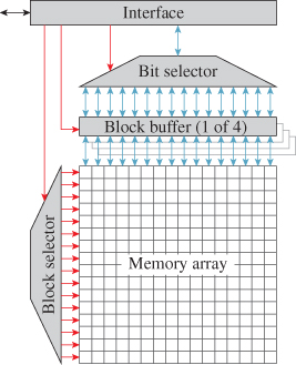
Figure 38.8: Block diagram of a simplified GDDR3 memory circuit. For increased clarity, the true storage capacity (one billion bits) is reduced to 256 bits, implemented as an array of sixteen 16-bit blocks (a.k.a. rows). The red arrows arriving at the left edges of blocks indicate control paths, while the blue ones meeting the tops and bottoms of blocks are data paths.
While early DRAMs hid this complexity behind a simple interface protocol, modern DRAMs expose their internal resources and operations.12 The GDDR3 DRAM used by the GeForce 9800 GTX, for example, implements four separate block buffers, each of which can be loaded from the memory array, modified, and written back to the array as individually specified, and in some cases concurrent, operations. Thus, the circuit connected to the GDDR3 DRAM does more than just read or write bits—it manages the memory as a complex, optimizable subsystem. Indeed, the memory control circuits of modern GPUs are large, carefully engineered subsystems that contribute greatly to overall system performance.
12. Using the terminology of this chapter, DRAM architecture has evolved to more closely match DRAM implementation.
But what performance is optimized? In practice, the DRAM memory controller cannot simultaneously maximize bandwidth and minimize latency. For example, sorting requests so that operations affecting the same block can be aggregated minimizes transfers between the block buffers and the array, thereby optimizing bandwidth at some expense to latency. Because the performance of modern GPUs is frequently limited by the available memory bandwidth, their optimization is skewed toward bandwidth. The result is that total memory latency—through the memory controller, to the DRAM, within the DRAM, back to the GPU, and again through the memory controller—can and does reach hundreds of computation cycles. This observation is our second hardware principle.
The primary challenge of memory is coping with access latency and limited bandwidth. Capacity is a secondary concern.
The way that GPUs such as the GeForce 9800 GTX handle this (sometimes) huge memory latency is the subject of the next subsection.
38.6.3. Coping with Latency
Consider again the fragment shader of Listing 38.2. Ignoring execution of the tex1D instruction, this shader makes five floating-point assignments and performs four floating-point multiplications, for a total of nine operations. Again, ignoring texture interpolation, we would expect its execution to require approximately ten clock cycles, perhaps fewer if the GPU’s data path implementation supports hardware parallelism for short vector operations. (The GeForce 9800 GTX data path does not.) Unfortunately, even if the GPU implementation provides separate hardware for the computations required by image interpolation (the GeForce 9800 GTX, like most modern GPUs, does) the execution time of the texture-based fragment shader could increase to hundreds or even thousands of cycles due to the latency of the memory reads required to gather the values of the texels. Thus, the performance of a naive implementation of this shader could be reduced by a factor of ten to one hundred, or more, due to memory latency.
There are three potentially legitimate responses to this situation: 1) accept it; 2) take further steps to reduce memory latency; or 3) arrange for the system to do something else while waiting on memory. Of course, options (2) and (3) may be combined.
The engineering option of accepting a nonoptimal situation must always be considered. Just as code optimization is best directed by thorough performance profiling, hardware optimization is justified only by a significant improvement in dynamic (i.e., real-world) performance. If texture interpolation were extremely rare, its low performance would have little real-world effect. In fact, texture interpolation is ubiquitous in modern shaders, so its optimization is of paramount concern to GPU implementors. Something must be done.
Once the memory controller has been optimized, further reduction of memory latency may be achieved by caching. Briefly, caching augments a homogeneous, large (and therefore distant and high-latency) memory with a hierarchy of variously sized memories, the smallest placed nearest the requesting circuitry, and the largest most distant from it. All modern GPUs implement caching for texture image interpolation. However, unlike CPUs such as the Intel Core 2 Extreme QX9770, which depend primarily on their large (four-level) cache systems for both memory bandwidth and latency optimization, GPU caches are large enough to ensure that available memory bandwidth is utilized efficiently, but they are too small to adequately reduce memory latency. We leave further discussion of the important topic of caching to Section 38.7.2.
Because options (1) and (2) do not adequately address latency concerns, the performance of GPUs such as the GeForce 9800 GTX depends heavily on their implementation of option (3): arranging for the GPU to do something else while waiting on memory. The technique they employ is called multithreading. A thread is the dynamic, nonmemory state (such as the program counter and register contents) that is modified during the execution of a task. The idea of multithreading will not be new to you—it’s related to ideas already discussed in Section 38.4. There we learned that the (architecturally specified) programmable vertex, primitive, and fragment processing stages are implemented with a single computation engine that is shared between these distinct tasks. Multithreading is the name of such a virtual-parallel implementation. When multiple tasks share a single processor, the thread of the currently executing task is stored (and modified) in the program counter and registers of the processor itself, while the threads of the remaining tasks are saved unchanged in thread store. Changing which task is executing on the processor involves swapping two threads: The thread of the currently active task is copied from the processor into thread store, and then the thread of the next-to-execute task is copied from thread store into the processor.
Multithreading implementations are distinguished by their scheduling techniques. Scheduling determines two things: when to swap threads, and which inactive thread should become active. Interleaved scheduling cycles through threads in a regular sequence, allocating a fixed (though not necessarily equal) number of execution cycles to each thread in turn. Block scheduling executes the active thread until it cannot be advanced, because it is waiting on an external dependency such as a memory read operation, or an internal dependency such as a multicycle ALU operation, and then swaps this thread for a thread that is runnable. Two queues of thread IDs are maintained: a queue of blocked threads and a queue of runnable threads. When a thread becomes blocked its ID is appended to the blocked queue. IDs of threads that become unblocked are moved from the blocked queue to the run queue as their status changes.
GPUs such as the GeForce 9800 GTX implement multithreading with a hierarchical combination of interleaved and block scheduling. The GeForce 9800 GTX hardware enables zero-cycle replacement of blocked threads: No processor cycles are lost during swaps. Because there is no performance penalty for swapping threads, the GeForce 9800 GTX implements a simple static load balancing by swapping every cycle, looping through the threads in the run queue. Load balancing between tasks of different types—vertex, primitive, and fragment—is implemented by including different proportions of these tasks in the mix of threads that is executed on a single core. This per-thread-group load balancing (the mix can’t be changed during the execution of a group of such threads) is adjusted from thread group to thread group based on queue depths for the various task types.
Threads are small by the standards of DRAM capacity—on the order of 2,000 bytes each (roughly 128 bytes per vector element). This suggests that thread stores would contain large numbers of threads, but in fact they do not. The GeForce 9800 GTX, for example, stores a maximum of 48 threads per processing core in expensive, on-chip memory. Once again memory latency is the culprit. To support zero-cycle thread swaps, there must be near-immediate access to threads on the run queue. Thus, thread store must have low latency, and is necessarily small and local. (In fact, the GeForce 9800 GTX stores all threads in a single register file. Threads are not swapped in and out at all; instead, the addressing of the register is offset based on which thread is being executed.) More generally, because multithreading compensates for DRAM latency, it is impractical for its implementation to experience (and be complicated by) that same latency. Thus, thread store is an expensive and scarce resource.
Because thread store is a scarce resource whose capacity has a significant effect on performance (the processor remains stalled while the run queue is empty) optimizations that reduce thread storage requirements are vigorously pursued. We discuss two such optimizations, both of which are implemented by the GeForce 9800 GTX.
First we consider thread size. Because register contents constitute a significant fraction of a thread’s state, the size of a thread can be meaningfully reduced by saving and restoring only the contents of “active” registers. In principle, register activity could be tracked throughout shader execution so that thread-store usage varied depending on the program counter of the blocked thread. In practice, thread size is fixed, throughout the execution of a shader, to accommodate the maximum number of registers that will be in use at any point during its execution. Because the shader compiler is part of the GPU implementation (recall that shader architecture is specified as a high-level language interface) the implementation not only knows the peak register usage, but also can influence it as a compilation optimization.
Thread size matters because the finite thread store holds more small threads than large ones, decreasing the chances of the run queue becoming empty and the processor stalling. While this relationship is easily understood, programmers are sometimes surprised when their attempt to optimize shader performance by minimizing execution length (the number of instructions executed) reduces performance rather than increasing it. Typically (compiled) shader length and register usage trade off against each other—that is, shorter, heavily optimized programs use more registers than longer, less optimized ones—hence, the counterintuitive tuning results. Modern GPU shader compilers include heuristics to optimize this tradeoff, but even experienced coders are sometimes confounded.
Performance may also be optimized by running threads longer, thereby keeping more threads in the run queue. A naive scheduler might immediately block a thread on a memory read (or an instruction such as tex1D that is known to read data from memory) because it is rightly confident that the requested data will not be available in the next cycle. But the requested data may not be required during the next cycle—perhaps the thread will execute several instructions that do not depend on the requested data before executing an instruction that does. A hardware technique known as score boarding detects dependencies when they actually occur, allowing thread execution to continue until a dependency is reached, thereby avoiding stalls by keeping more threads in the run queue. It is good programming practice to sequence source code such that dependencies are pushed forward in the code as far as possible, but shader compilers are optimized to find such re-ordering opportunities regardless of the code’s structure.
While hiding memory latency with multithreaded processor cores is a defining trait of modern GPUs, the practice has a long history in CPU organization. The CRAY-1 did not use multithreading, but the CDC 6600, an early-1960s Seymour Cray design that preceded the CRAY-1, did [Tho61]. It included a register barrel that implemented a combination of pipeline parallelism and multithreading, rotating through ten threads, each at a different stage in the execution of its ten-clock instruction cycle. The Stellar GS 1000, a graphics supercomputer built in the late ’80s, executed four threads in a round-robin order on its vector-processing main CPU, which also accelerated graphics operations [ABM88]. Most Intel processors in the IA-32 family implement “hyperthreading,” Intel’s branded version of multithreaded execution.
38.7. Locality
A common rule of thumb is that programs spend 90% of their time running only 10% of their program code. The 90/10 rule is an approximation—for example, code percentages varied between six and 57 in tests reported by John Hennessy and David Patterson [HP96]—but it suggests an essential truth, which is that the outcomes of computing events, such as generating an address or taking a branch, are not evenly distributed. Instead, these events, when treated as random variables, have probability distributions that are unfair (meaning that outcomes have different probabilities) and dependent (meaning that the probability distributions themselves change with the history of recent events).
An unfair coin is undesirable, but unfair and dependent probability distributions in computing are an important opportunity—they allow system designers to make optimizations that dramatically improve performance and efficiency. In computer science the term locality describes the nature of the unfair, dependent probability distributions that are observed in functional computing systems. In this section we define various forms of locality and study how system designers take advantage of them.
38.7.1. Locality of Reference
In treating memory abstractly as an ordered array of items, two observations have been made about the patterns of access to these items during the execution of a program. First, an item that has been accessed recently has an increased probability of being accessed again. This program property is called temporal locality. Second, items whose addresses are similar tend to be accessed close together in time. This program property, though it is also time-dependent, is called spatial locality to emphasize its application to multiple items. Together, temporal and spatial locality constitute locality of reference.
While locality of reference is observed in all computing systems, design decisions significantly affect how much is observed. Consider the sequence in which instructions are fetched. A computer could be designed such that each instruction specified the address of the subsequent instruction, allowing execution to skip arbitrarily through the code. But this approach is never taken.13 Instead, designers universally choose to execute instructions sequentially, except in the special case of branching. This choice directly increases spatial locality in an obvious way. Because most branches cause short sequences of instructions to be repeated (i.e., they loop), sequential instruction fetching also increases temporal locality. Indeed, this single decision frequently ensures that locality of reference is greater for instruction accesses than it is for data accesses, despite designers’ attempts to increase the latter.
13. To this author’s knowledge. But partially randomized execution sequences are now employed as a security measure, to thwart the attempts of computer “hackers.”
Because GPU shaders are typically much smaller than the data structures they access, GPU designers are more concerned with data locality than they are with code locality. An example of a design decision that greatly affects GPU data locality is the way that 2D texel coordinates, which specify a single texel in a 2D texture image, are mapped to the (1D) memory addresses of the texel-data storage locations. When fragments generated by the rasterization of a small triangle are textured, their 2D texel coordinates typically cluster into a small region in the texture image. Data locality will be greater if the 1D memory addresses of the texels that are accessed also cluster into a small band of locations.
Let (x, y) be the 2D integer coordinates of a texel in a square texture image of dimension w, and a0 be the base address of the texture data in memory. Then an obvious mapping would be raster order, specified as
Unfortunately Equation 38.1 results in a single tight cluster of memory addresses only if y is single-valued. If the patch of texels is not on a single scanline of the texture image, different values of y produce smaller clusters of addresses, themselves separated by intervals of texture dimension w. Because w can be large (e.g., 1,024 or even 4,096) the overall clustering is not tight at all.
Spatial locality can be greatly improved by replacing the raster-order mapping of Equation 38.1 with tiled mapping. The texture image is logically divided into smaller squares that tile the image, meaning that they cover the image with no gaps and no overlaps. Tiled mapping is hierarchical: first raster order among tiles, then raster order within the selected tile. Given a tile dimension of wt, the mapping is specified as
where ÷ indicates truncated integer division (e.g., 7 ÷ 4 = 1) and ![]() indicates modulo division yielding the remainder (e.g., 7
indicates modulo division yielding the remainder (e.g., 7 ![]() 4 = 3). If the accessed texels fall within a single tile (i.e., among all the address mappings, only the last two terms of the equation differ) then spatial locality is improved by a factor of w/wt, because the small clusters of memory addresses are separated by wt (which multiplies y in the final expression in Equation 38.2) rather than w (which multiplies y in Equation 38.1). Decreasing the tile size increases the magnitude of the improvement: 8 × 8-texel tiling of a 2,048 × 2,048-texture image improves spatial locality by a factor of 256! But smaller tiles also increase the likelihood that the cluster of texels will straddle multiple tiles, which drives locality back down, potentially below its raster-mapped value, if vertically adjacent tiles are straddled and the 2D cluster of texels is small. Finding the best balance among such tradeoffs is central to the art of system design. One clever solution increases the depth of the hierarchy by implementing tiles within tiles, or even tiles within tiles within tiles. Of course, this approach runs into limits of complexity as the depth of the hierarchy is increased, introducing yet another tradeoff.
4 = 3). If the accessed texels fall within a single tile (i.e., among all the address mappings, only the last two terms of the equation differ) then spatial locality is improved by a factor of w/wt, because the small clusters of memory addresses are separated by wt (which multiplies y in the final expression in Equation 38.2) rather than w (which multiplies y in Equation 38.1). Decreasing the tile size increases the magnitude of the improvement: 8 × 8-texel tiling of a 2,048 × 2,048-texture image improves spatial locality by a factor of 256! But smaller tiles also increase the likelihood that the cluster of texels will straddle multiple tiles, which drives locality back down, potentially below its raster-mapped value, if vertically adjacent tiles are straddled and the 2D cluster of texels is small. Finding the best balance among such tradeoffs is central to the art of system design. One clever solution increases the depth of the hierarchy by implementing tiles within tiles, or even tiles within tiles within tiles. Of course, this approach runs into limits of complexity as the depth of the hierarchy is increased, introducing yet another tradeoff.
We’ve just seen how the implementation of a GPU, through tiled texel mapping, can improve spatial locality. GPU architectures—that is, their programming interfaces—can also be designed to allow improved locality of reference. For example, the OpenGL programming interface couples each texture image with its texture reconstruction-filtering mode, allowing the GPU driver to select image-tiling parameters based on details such as linear versus cubic filtering. The Direct3D interface allows a single texture image to be used with several texture interpolation modes. This choice gives programmers more flexibility (they can use a single texture image for multiple purposes that require different interpolations) but constrains optimizations by the GPU driver (e.g., a compromise tiling of the texture image may be chosen).14
14. OpenGL versions 3.3 and later have adopted the Direct3D approach of decoupling texture images and interpolation modes.
38.7.2. Cache Memory
We’ve discussed what data locality is, and seen some examples of how GPU architecture and implementation are designed to increase data locality. Now we’ll see how data locality can be exploited by system designers to greatly improve the performance of computing systems.
Recall from Section 38.6.2 that latency and bandwidth, the two greatest concerns of a memory-system designer, are inversely related to memory capacity: Smaller memories have lower access latency and higher access bandwidth, that is, they are faster than larger memories. Because locality of reference makes it likely that, for a given short window of time, most memory accesses are to a small number of physical memory blocks, we can improve performance by storing these blocks in a smaller, faster memory. There are two ways to expose this local memory: explicitly and implicitly.
The explicit approach directly exposes local memory in the architecture, giving programmers complete control of its use. Address fields of explicit local memory (which is small) require fewer bits than addresses for the main memory system (which is large), so their use reduces the bit rate of the processor instruction stream, as well as benefitting from reduced latency and increased bandwidth to the specified data. Registers are an extreme form of explicit local memory: They require very small addresses, and they exhibit negligible latency and huge bandwidth. The local memory blocks in Figure 38.3 are a more typical form of explicit local memory. Because these memories are not visible in either the OpenGL or the Direct3D pipeline models, we defer discussion to Section 38.9.
Although registers are explicit in the Direct3D architecture, their allocation and use is managed by the shader compiler rather than by programmers. In principle, shader compilers could also manage and optimize the use of other local memory, but in practice this is left to human programmers. Programmer-specified management of local memory is powerful, but it is also complex, time-consuming, and error-prone. Thus, it is desirable to provide a form of local storage that is managed implicitly and automatically by low-level (typically hardware-implemented) mechanisms within the architecture. We refer to such local memory as cache (pronounced “cash”) memory.
Cache memory intercepts all accesses to main memory. If the requested data item is already present in the cache, it is either returned with low latency (in the case of a read request) or modified in place (in the case of a write request). If the requested item is not present in the cache, some previously cached item is evicted, the requested item is read from main memory into the cache, and then either returned with high latency (in the case of a read request) or modified in place (in the case of a write request). All of this happens implicitly, without programmer intervention, so there is no opportunity for programmer error. But programmers can significantly influence performance by coding to maximize data locality, since accesses of main memory are so costly.
Read requests that are fulfilled by cached data (cache hits) have dramatically lower latency than those fulfilled from main memory (cache misses). Taking main-memory latency as the benchmark, this disparity is desirable: If most memory requests hit, latency is dramatically reduced. But it is tempting instead to take the cache’s hit latency as the benchmark, because this performance is achieved asymptotically as the cache-miss rate goes to zero. Unfortunately, the large disparity in latencies is undesirable from this viewpoint, because even a few misses dramatically increase average latency. For example, the average latency of a cache with a miss penalty of 100x is doubled by a miss rate of only 1%. In practice, only very large cache memories achieve average read latencies that approach this hit latency.
Cache memory is organized into equal-size units called lines, which are typically much larger than a single data item. Transfers between the processor and cache memory operate at the granularity of individual data items—a word is read from a line in the cache and returned to the processor, or a byte is written from the processor into the appropriate cache line. But transfers between cache and main memory operate at cache-line granularity—entire cache lines are either read from or written to main memory. Cache-line size is chosen so that these transfers make efficient use of main-memory bandwidth. For example, cache lines may be as large as the blocks in main memory, or at least a substantial fraction of this size. When a cache read miss forces a line to be loaded from main memory, spatial locality ensures that most if not all of the data items in that line will be accessed before the line is overwritten by another. And caches can be designed to transfer lines back to main memory infrequently (write-back cache) rather than immediately after the processor writes a data item to the cache (write-through cache), minimizing the main-memory bandwidth consumed by writing, and thereby maximizing the main-memory bandwidth available for reading.
From the standpoint of the processor, cache memory addresses both of the key concerns of main memory: Apparent memory latency is reduced, and apparent memory bandwidth is increased. If cache memory size could be made arbitrarily large, both apparent latency and apparent bandwidth could in principle be driven to the point of diminishing return (i.e., to the point where further improvement would not increase processor performance). In practice, cache size is limited to a small fraction of the size of main memory, after which cache performance slows to that of main memory. Because apparent latency increases quickly even for very low miss rates, GPU implementations are typically tuned to achieve performance that is unconstrained by memory bandwidth (assuming typical graphics loading) with caches that are far too small to ensure the required latency. The (otherwise unacceptable) apparent memory latency is hidden by multithreading, as described in Section 38.6.3, rather than by outsized cache memories.
It is still possible for shader programmers to get in trouble, though, by demanding more memory bandwidth than is available. For example, GPU texture interpolation performance is typically balanced assuming high data locality. If this assumption is disrupted—if, for example, texture sample addresses specify disjoint, widely separated clusters of texels—then an excessively large number of memory blocks may be transferred from main memory to cache memory, and shader performance can plummet. Undersampling a texture is one way to create this situation. Thus, texture aliasing not only destroys image quality, it can also destroy GPU performance! Dependent texture reads, meaning calls to tex1D, tex2D, or tex3D, with a parameter that is not directly derived from the triangle-interpolated texture coordinates, can also disrupt or destroy locality. The resultant complications contributed to the delay of support for dependent texture lookup, which was introduced to GPUs years after shader programmability was first supported.
Thus far we have considered a single cache memory, but modern GPUs often have two levels of cache, and CPUs even more (three, sometimes four). By convention these are named L1 cache, L2 cache, . . . Ln cache, counting outward from the processor toward main memory.15 L1 cache has the least capacity, but also the least latency, and is optimized to interact well with the processor. Ln cache has the greatest capacity and the highest latency, and is optimized to interact well with main memory. Worst-case latency may actually increase as levels of memory hierarchy are added, due to the summation of multiple miss penalties, but overall performance is improved.
15. Abbreviations L1$, L2$, . . . Ln$ are sometimes used informally, such as in figures.
In systems with multiple processor cores, caching is typically also parallelized. The GeForce 9800 GTX GPU, for example, implements a separate L1 cache for each pair of cores, and a separate L2 cache for each bank of memory (see Figure 38.4). Multiple L1 caches allow each to be tightly coupled with only two processor cores, reducing latency by improving locality (each cache is physically closer to its cores) and by reducing access conflicts (each cache receives requests from fewer cores). Pairing an L2 cache with each memory bank allows each cache to aggregate accesses that map to its portion of main memory. Explicit local memory is also parallelized—the GeForce 9800 GTX implements a separate local memory for each core.
Recall that a key advantage of implicit local memory is the simplicity and reliability of its programming model. Adding hierarchy does not compromise this model: Although a single physical memory location may now be cached at multiple levels of the memory hierarchy, memory requests from multiple cores “see” a consistent value because the requests are handled consistently. Parallel caches (such as multiple L1 caches) potentially break the model, however, because they are accessed and updated independently, so replications of a single physical memory location can become inconsistent. If this happens, the programmer’s model of the memory system has become incoherent, and the likelihood of programming errors skyrockets.
Architects of parallel systems handle the cache coherence problem in one of three ways.
1. Coherent memory: A coherent view of memory is enforced by adding complexity to the memory hierarchy implementation. Cache-coherent protocols ensure that changes made to one data replica are broadcast or otherwise transferred to other replicas, either immediately or as required. This solution is expensive, both in implementation complexity and in the inevitable reduction in performance.
2. Incoherent memory: An incoherent view of memory is accepted—programmers must contend with the additional complexity this entails. This solution is frugal in system implementation, but it is expensive due to the likely reduction in programmer efficiency.
3. Constrained access: A coherent view of memory is enforced by constraining how memory is accessed, rather than by adding complexity to the memory hierarchy implementation. This is the approach taken by GPUs as they are exposed by the Direct3D and OpenGL interfaces. Memory that is shared, such as texture images, is read-only, so no inconsistencies are possible. Memory that is written, such as framebuffer memory, is write-only from the viewpoint of the parallel cores—read-modify-write framebuffer operations, such as depth buffering and blending, are implemented by dedicated “pixel ops” circuits that operate directly on framebuffer physical memory (see Figure 38.4). So again, no inconsistency is possible.
Cache memory is a central concern in computer architecture, and we have only scratched the surface in this short section. Rich topics, such as eviction policy and set associativity, have not been covered at all. Interested readers are encouraged to peruse the list of suggested readings at the end of this chapter. Be warned, however, that most of the literature is written from the perspective of CPU architects, whose experience and consequent world views differ from those of GPU architects.
38.7.3. Divergence
We learned in Section 38.4 that GPUs such as the GeForce 9800 GTX implement a SPMD programming model with SIMD processing cores. The single-program, multiple-data programming model allows shaders to be written as though each was executed individually, greatly simplifying the programmer’s job. The single-instruction, multiple-data implementation collects elements (e.g., vertices, primitives, or pixel fragments) into short vectors, which are executed in parallel by data paths that share a single instruction sequence unit. (The GeForce 9800 GTX has 16 cores, each with an effective vector length of 16 elements.)
The motivation for SIMD implementation is efficiency: Sharing a single instruction stream among multiple data paths allows more data paths to be implemented in the same silicon area and reduces instruction-fetch bandwidth per data path. For example, if a core’s instruction sequence unit occupies the same silicon area as one data path, then a 16-wide true-parallel SIMD core occupies just over half (17/32) the area required by 16 SISD cores, almost doubling peak performance per unit silicon area. But this efficiency is achieved only when the elements assigned to a vector require the same sequence of instructions. When different sequences are required—that is, when the instruction sequences diverge—efficiency is lost.
When GPU shader programming was first exposed in OpenGL and Direct3D, shaders had no conditional branch instructions. Each instance of such a shader executed the same sequence of instructions, regardless of the element data being operated on, so divergence was limited to vectors that straddled a change made to a shader. Then, as now, GPU architectures encouraged operations on large blocks of data (e.g., Direct3D vertex buffers and OpenGL vertex arrays), during which no changes can be made to shaders. And GPU implementations typically packed SIMD vectors first-come-first-served, just as skiers are loaded onto lift chairs. So vectors that straddled changes in shaders were unusual, and divergence was not a significant problem.
Modern GPUs do support conditional branching in shaders, however, and its use by programmers does increase divergence. In the worst case, when each vector element executes a completely different program section (e.g., the shader is equivalent to a C++ switch statement with selection driven by unique element indices) divergence is complete and all parallelism is lost. More typically, elements share portions of code, which the predicated SIMD core executes in parallel, so parallelism is merely reduced.
Figure 38.9 illustrates such a typical situation, using a simplified four-element vector core. Shader A includes a single conditional branch that selects either the two-operation no path or the four-operation yes path. Another four operations, two ahead of the branch and two after, are common to both paths: They are executed regardless of which path is taken. In the first example, B, all four elements take the no branch, so there is no divergence. Predication handles this case by executing each common no-path operation in parallel across the four-wide vector. Because no elements require the yes-path operations, they are never executed and no cycles are lost to them. Thus, the entire shader executes in only six cycles.
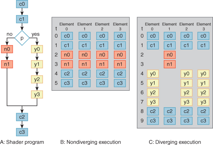
Figure 38.9: Diverging and nondiverging execution on a four-element predicated vector core. Each element executes the ten-operation shader A that branches on predicate p. In case B, all four elements take the no branch, there is no divergence, and only six execution steps are required. In case C, element one takes the no branch, but the other three elements take the yes branch. Predication handles this divergence by executing the no and yes operations separately, so all ten execution steps are required.
In the second example, C, element one takes the no branch, but the other elements take the yes branch. Because both branches are taken, execution diverges. Predication handles this divergence by first executing each no operation on the single element that requires it, then executing each yes operation in parallel across the three elements that require it. Because both no and yes operations are executed, shader execution requires the full ten cycles to complete.
Obviously, divergence reduces the efficiency of computation on a predicated SIMD core. We quantify this loss by computing utilization: the ratio of the useful work that is done to the number of operation slots made available for that work. Let n be the vector’s length, ipred be the number of predicated instruction steps required to execute the vector to completion, and iseq be the total number of instruction steps that would be required to execute the element’s shaders sequentially, one at a time, as though on a single processor. Then the utilization of this vector’s execution (uvec) is the ratio of useful work done (iseq) to the number of slots available for that work (n · ipred):
In example B, the nondiverging case,
which is the maximum possible value, indicating full utilization. In example C, the diverging case,
indicating partial utilization. Predication ensures that an operation is executed for at least one element during each cycle, so the worst possible utilization for an n-wide vector core is 1/n. Minimum utilization is achieved in the switch-statement situation described above; it is approached asymptotically when a single element executes a path that is much longer than the paths executed by the other elements.
Utilization directly scales performance—the 0.75 utilization achieved in example C corresponds to 75% of peak performance, or 33% additional running time (when aggregated across many elements). Because poor utilization is the direct result of divergence, it is useful to understand the likelihood of divergence, perhaps as a first step to minimizing it.
Again consider a shader with a single conditional branch. Let p be the branch’s probability of taking the yes path, and 1 – p be its probability of taking the no path. Then, if p is evaluated independently for each element, that is, if evaluations of p had no locality, then divergence outcome probabilities for an n-wide vector core are:
Unless p is either very near to zero or very near to one, the probability of diverging increases rapidly as vector length n increases. For example, the probability of divergence with p = 0.1 is 34% for n = 4, but it increases to 81% for n = 16, 97% for n = 32, and 99.9% for n = 64. Even with p = 0.01, a seemingly low probability, divergence occurs almost half the time (47%) for a vector length of 64. These odds might dissuade GPU architects from implementing wide vector units if they were correct, but in general they are not.
In fact, evaluations of p are not independent—they tend to cluster into yes groups and no groups. Temporal locality predicts this: Clusters of repeated references suggest that the same code branch is executed repeatedly. The geometric nature of computer graphics often strengthens the effect. Consider the typical case of a predicate p that is true in shadow and false otherwise. Some triangles will be partially shadowed, but unless tessellation is very coarse, most will be either fully lighted or fully in shadow. The stream of fragments resulting from the rasterization of these triangles will therefore have long clusters of same-valued predicates. And SIMD vectors loaded with these fragments will experience low divergence.
Just as GPU designers manipulate the texel-to-memory mapping to improve spatial locality during texture mapping (see Section 38.7.1), they also manipulate the sequence in which fragments are generated during rasterization. Rather than generating the fragment stream from a raster path, a more complex 2D path (akin to a space-filling curve) is often employed (see Figure 38.10). For triangles that project to a small region in the framebuffer this ordering makes little difference. But for larger triangles it substantially improves the 2D locality in the pixel coordinates of the generated fragments. This locality reduces SIMD divergence in the same way that rasterizing small triangles does. It has the added benefit of improving the spatial locality of texture coordinates, and therefore of the memory accesses required to perform texture mapping.
38.8. Organizational Alternatives
GPU architectures are specified at the relatively high levels of Direct3D and OpenGL, leaving implementors plenty of room for innovation. But not endless room—there exist attractive design alternatives that test and sometimes exceed this limit. Three such alternatives are considered in this chapter: deferred shading, binned rendering, and CPU/GPU-hybrid implementation. All have been implemented in earlier research or production systems, some are employed in current embedded or mobile systems, and all have desirable properties that make them likely candidates for future systems.
38.8.1. Deferred Shading
The goal of deferred shading is to shade only visible samples, thereby minimizing shading costs.16 Because Direct3D and OpenGL determine visibility in the framebuffer, using the z-buffer algorithm, visibility is fully resolved only after the entire scene has been rendered. So shading must be deferred until this time, and rendering becomes a two-phase process: Render the entire scene to the frame-buffer, and then compute shading for each pixel in the framebuffer. Furthermore, because shading requires access to various parameters that are interpolated during rasterization—such as surface normals, material parameters, and texture names—these values must be rendered into and stored in the framebuffer.
16. Shading as it is treated here considers only light that reaches surface samples directly, not light that is reflected from other surfaces. This is a typical simplification in high-performance graphics rendering.
In addition to reducing the number of shading calculations, deferred shading also alters the locality of the shading calculations. Consider an implementation that executes shaders on screen-aligned tiles of pixels. Individual triangles are often split across tile boundaries, so per-tile deferred shading reduces the inherent locality of triangle calculations. But the set of triangles rendered to a tile have a locality in 3D space that can allow lighting to be optimized. Specifically, many lights in a highly lighted scene can be culled, because they are too far from the 3D region corresponding to the tile. In scenes with thousands of lights the performance balance can tilt toward deferred shading.
Difficulties with deferred shading include the following.
• Excess storage and bandwidth: Burdening each pixel in the framebuffer with the information required for its shading is a significant expense in both storage and bandwidth. Indexing helps: Textures can be specified by reference; even better, the entire shader can be specified by reference. But parameters such as surface normals and interpolated texture coordinates are specific to each pixel, so they require storage by value. Variability in storage requirements complicates the situation, because maximum per-pixel storage requirement is not easily inferred at the start of rendering, and neither Direct3D nor OpenGL requires that it be specified.
• Incompatibility with multi-sample anti-aliasing (MSAA): Multi-sample anti-aliasing, the currently preferred approach to reducing edge artifacts in full-scene rendering, requires storage for multiple color and depth samples at each pixel. For example, multi-sample anti-aliasing with four samples per pixel increases framebuffer storage requirements by a factor of four. In combination with deferred shading, multi-sample anti-aliasing increases already burdensome framebuffer storage requirements by this same factor. Shading calculations are also increased by this factor, undoing the central optimization of multi-sample anti-aliasing, which is limiting shading calculations to one per pixel. The real possibility of a net increase in shading calculations, and the certainty of increased storage, make deferred shading incompatible with multi-sample anti-aliasing.17
17. At the time of this writing, researchers are actively investigating deferred-shading algorithms that are compatible with multi-sample anti-aliasing.
• No shader-specified visibility: High-performance rendering sometimes approximates the visibility of complex geometry, such as foliage, with an alpha matte rendered as a texture. This optimization is inconsistent with deferred shading, whose goal is full determination of visibility prior to shading.
Against this seemingly bleak background, the story of deferred shading has a surprisingly happy ending. All modern GPUs, including the GeForce 9800 GTX, implement an optimization called early z-cull. An outline of the algorithm follows. As the frame is rendered, the GPU builds a hierarchical structure of z-values in dedicated local memory. Rasterized fragments are tested against this z-pyramid and are either culled (prior to shading) if they are not visible, or delivered to the framebuffer (and added to the z-pyramid) if they are visible. Little extra storage, and no main-memory bandwidth, are required, yet much of the performance gain of deferred shading is achieved, especially when programmers deliver scene data in an order that approximates front to back (i.e., rendering objects that are progressively farther from the viewpoint). While exact front-to-back ordering is a huge burden to programmers, approximating this ordering is often straightforward, and the penalty for partial failure is low (just a slight decrease in performance). Alternatively, application programmers sometimes choose to render the entire scene twice—first with shading disabled to create the full z-pyramid, and then again with shading enabled to shade exactly the visible fragments—to fully achieve deferred shading. Of course, early z-cull doesn’t optimize computational locality for scenes with thousands of lights, so GPU architects will continue to study approaches to true deferred shading.
Suppose that the depth complexity of a pixel is n (i.e., a ray traced through the pixel would intersect n different surfaces in the scene, only the nearest being visible), and that these surfaces are processed in random order, but with early z-cull, that is, a fragment is shaded only if it’s in front of all other fragments we’ve encountered so far. What’s the expected number of fragments that are shaded during the course of rendering this pixel?
38.8.2. Binned Rendering
We usually define rasterization as the process that converts screen-coordinate geometric primitives directly to pixel fragments. But rasterization to larger screen areas, such as to n × n-pixel tiles, is also possible. The GeForce 9800 GTX rasterizer is a case in point—it outputs 2 × 2 quad fragments to simplify texture-mapping calculations, as described in Section 38.6.1. Binned rendering splits rasterization into two phases: a first phase that outputs medium-size tile fragments, each corresponding to a (typically) 8 × 8-, 16 × 16-, or 32 × 32-pixel grid in screen coordinates, followed by a second phase that reduces each tile fragment to pixel fragments. Of course, tile fragments include information derived from the screen-coordinate primitive so that second-phase rasterization can produce the correct pixel fragments.
Binned rendering actually splits the entire rendering process into two phases, corresponding to the two phases of rasterization. During the first phase the scene is processed through tiled rasterization, and the resultant tile fragments are sorted into bins, one bin corresponding to each screen tile. Only after the first phase is completed (i.e., after tile fragments for the entire scene have been generated and sorted into bins) does the second phase begin. During the second phase each bin is processed individually to completion, yielding an n × n tile of pixels that is deposited in the framebuffer.
Binned rendering has several attractive properties.
• Local memory: The absolute guarantee of framebuffer data coherence—only pixels within the tile are accessed—allows pixels to be processed in local memory, rather than cached from main memory. Both power and main-memory cycles are conserved, making binned rendering an attractive solution for mobile devices.
• Full-scene anti-aliasing: Recall that multi-sample anti-aliasing requires storage for multiple color and depth samples at each pixel. As quality is improved by increasing the sample count, both storage and bandwidth become prohibitively expensive when rendering is to the entire frame-buffer, but they remain economical when rendering is limited to a small tile of pixels. Even more advanced rendering algorithms, such as order-independent rendering of transparent surfaces, can be supported with clever use of local memory.
• Deferred shading: Limiting rendering to a small tile of pixels addresses the key limitations of deferred shading: its requirements of excessive memory storage and bandwidth, and its incompatibility with multi-sample anti-aliasing.
The advantages of binned rendering are compelling, yet no current PC-class GPU implements it.18 The fundamental reason is that binned rendering differs too much from the pipeline Direct3D and OpenGL architectures—we say that the abstraction distance is too large. Typically, excess abstraction distance results in products with confounding performance characteristics (operations expected to be fast are slow; those expected to be slow are fast) or subtle deviations from specified operation. Practical problems that are encountered include the following.
18. Inexpensive Intel GPUs have implemented binned rendering in the past, but none do now.
• Excess latency: Previous binned rendering systems, such as the PixelPlanes 5 system developed at the University of North Carolina, Chapel Hill, have added a full frame time of latency.
• Poor multipass operation: Direct3D and OpenGL encourage advanced multipass rendering techniques that, in a binned implementation, require multiple two-pass operations per final frame. An example is rendering reflection from a curved surface by 1) rendering the scene that will be visible in the reflection, 2) loading this image as a texture, and 3) rendering the curved surface with the appropriately warped texture image. Some binned rendering systems failed to support such operations; others supported them, but performed poorly.
• Unbounded memory requirements: While binned rendering bounds pixel storage to that required for a single tile, the memory required by the bins themselves grows with scene complexity. Neither OpenGL nor Direct3D has scene-complexity limits, so a fully confirming implementation requires infinite memory (an obvious impossibility) or must introduce complexity to handle cases for which finite bin storage is inadequate.
These complications have been sufficient to keep binned rendering out of mainstream PC GPUs. But recent implementation trends, in particular the use of a time-shared single compute engine to implement all pipeline shading stages, may overcome some of the difficulties.
38.8.3. Larrabee: A CPU/GPU Hybrid
In 2008, Intel published a technical paper [SCS+08] describing a forthcoming GPU, code-named Larrabee. While this product never shipped, for reasons we will discuss shortly, it was a serious attempt to combine ideas from Intel CPUs and competitive GPUs into a single compelling product. In this short section we will analyze this hybrid GPU, first by comparing its implementation and architecture with those of the NVIDIA GeForce 9800 GTX GPU and the Intel Core 2 Extreme QX9770 CPU, and then by considering the resultant strengths and weaknesses. We begin with implementation, referring to the Larrabee block diagram in Figure 38.11, which is drawn to be consistent (where possible) with the NVIDIA GeForce 9800 GTX block diagram in Figure 38.4.
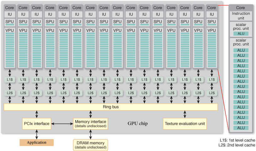
Figure 38.11: Intel Larrabee GPU block diagram. Compare this with the NVIDIA GeForce 9800 GTX GPU block diagram in Figure 38.4.
In several key respects the Larrabee implementation more closely resembles the implementation of the NVIDIA GeForce 9800 GTX GPU than it does that of the Intel Core 2 Extreme QX9770 CPU.
• Many cores: The Larrabee and GeForce 9800 GTX block diagrams are both dominated by multiple processing cores, as are the implementations of the GPUs themselves. While the number of cores in the Larrabee GPU was never announced, it is known to be at least 16, matching or exceeding the GeForce 9800 GTX, and greatly exceeding the four cores of the Core 2 Extreme QX9770 CPU. Furthermore, like the GeForce 9800 GTX cores, the Larrabee cores are designed to maximize performance per unit of silicon area (and therefore overall GPU performance), whereas the Core 2 Extreme QX9770 CPU cores are designed to maximize performance per core (at the expense of overall performance).
• Wide vectors: The Larrabee and GeForce 9800 GTX cores both include wide SIMD units: n = 8 for the GeForce 9800 GTX (virtualized to n = 16) and n = 16 for Larrabee. Both GPU cores provide hardware support for predication, and both provide separate address circuits for each element, allowing data to be efficiently gathered into a vector, then scattered back to memory. Conversely, the Core 2 Extreme QX9770 CPU implements narrow vectors (n = 4) with no support for efficient scatter/gather or predication.
• Texture evaluation: Both GPUs support texture evaluation with dedicated, fixed-function units; the CPU provides no support.
Balanced against these important similarities, the Larrabee and GeForce 9800 GTX implementations also differ in ways that betray Larrabee’s CPU heritage. These include the following.
• Specialized, fixed-function hardware: Except for its texture evaluation unit, Larrabee omits support for the many GeForce 9800 GTX fixed-function units, including vertex generation, primitive generation, fragment generation (rasterization), work queueing and distribution, and pixel operations.
• Latency hiding: Like the Core 2 Extreme QX9770 CPU, Larrabee relies more heavily on its large, hierarchical caches to hide memory latency.19 Each Larrabee core supports only four threads, against the 48 threads that implement the GeForce 9800 GTX’s block multithreading.20
19. Larrabee’s cache sizes are 64 Kbytes $L1 and 256 Kbytes $L2. While NVIDIA does not publish figures for the GeForce 9800 GTX, they are almost certainly much lower.
20. A technique called software fibers—explicitly coding a multithread instruction sequence into a single thread—is also used to hide latency. It lacks the GPU capability of block scheduling, however, and is therefore less effective.
• Cache coherence: Larrabee’s cache hierarchy maintains full coherence, just as the Core 2 Extreme QX9770 CPU’s caches do (though at somewhat higher cost, since Larrabee has at least four times as many caches at each level of the hierarchy). Cache coherence is not implemented by the GeForce 9800 GTX.
Larrabee’s strong implementation parallels to the GeForce 9800 GTX GPU are not matched in terms of architecture, where parallels to the Core 2 Extreme QX9770 CPU dominate.
• ISA: The Larrabee and Core 2 Extreme QX9770 cores share Intel’s IA-32 instruction set architecture (ISA), though Larrabee’s ISA is augmented with vector instructions. While the GeForce 9800 GTX cores are programmable, their ISA is hidden beneath the OpenGL and Direct3D shader languages. Both Larrabee and Core 2 Extreme QX9770 can be programmed to support OpenGL and Direct3D, and in fact Intel engineers ported both APIs to Larrabee (using binned rendering!), but these APIs are not architectural. Indeed, there is no evidence of a pipeline model in either CPU-like architecture.
• SPMD: Like the Core 2 Extreme QX9770, Larrabee cores are exposed in the ISA as scalar with vector instructions. Each core has 17 ALUs: one scalar and 16 vector. Programmers use a combination of scalar and vector instructions to explicitly manage control flow (a single program counter for the entire core) and vector operations on data. Predication is also explicit—programmers manipulate a mask to control which vector elements are committed. The GeForce 9800 GTX hides all this complexity behind its SPMD architecture, allowing programmers to treat each vector element as an individual execution unit with full flow control (its own program counter) and data execution capability.
Larrabee’s CPU-like architecture gives it important advantages over the GeForce 9800 GTX’s SPMD architecture.
• Flexibility: Larrabee executes arbitrary graphics algorithms with equal efficiency, because it isn’t optimized for a particular algorithm, as the GeForce 9800 GTX is for the “graphics pipeline.”
• Generality: Larrabee executes arbitrary nongraphics algorithms efficiently too.
• Capability: Like the Core 2 Extreme QX9770, Larrabee can run system-level programs up to and including operating systems. The GeForce 9800 GTX cannot.
But Larrabee’s flexibility, generality, and capability come at a cost: It is substantially more difficult to program than traditional GPUs such as the GeForce 9800 GTX. And, even with the heroic programming efforts of Intel’s experts, the resultant OpenGL and Direct3D implementations performed significantly less well than competitive, traditional GPUs. Larrabee’s more general architecture (ISA versus GeForce 9800 GTX’s SPMD) contributes to this situation, of course, but the relative lack of graphics specialization in Larrabee’s implementation is the root cause. While all graphics algorithms can be run on general-purpose vector cores, for some algorithms this is a very inefficient approach. Traditional GPUs such as the GeForce 9800 GTX are optimized to account for this: Independent, per-element operations with rich, application-programmable semantics such as those on vertices, primitives, and fragments are implemented on the data-parallel vector cores, while pipeline-specific algorithms with inherently rigid semantics such as rasterization (fragment generation) are implemented with specialized, fixed-function units.
Fixed-function units improve efficiency in several ways.
• Efficient parallelization: Specialized hardware can efficiently parallelize algorithms that are not inherently data-parallel.
• Correct provisioning: Algorithmic parameters such as numeric representation and precision can be optimized when the algorithm is implemented in task-dedicated hardware. Eight-bit integer multiplication, for example, requires less than one-tenth the hardware of 32-bit floating-point multiplication.
• Sequence optimization: When an algorithm is cast into dedicated hardware, each “step” is implemented with exactly the required capability (e.g., addition of two values) rather than effectively consuming the full capability of a core’s ALU (addition, subtraction, multiplication, division, etc.). Furthermore, the sequence of steps is managed with dedicated hardware (e.g., a simple finite-state machine) rather than expressed as a program running on a core’s instruction unit (whose stored-program model consumes expensive memory bandwidth and cache hierarchy).
All together, these advantages can yield impressive savings. For example, all modern GPUs include specialized hardware for decoding video streams.21 While video decoding can be implemented using the data-parallel cores, it reportedly consumes 1/100th the power when run in a purpose-designed unit, allowing laptop computers to display movies without quickly draining their batteries. Similar savings ratios may be achieved by fixed-function implementations of graphics pipeline stages.
21. This hardware is not otherwise discussed in this chapter.
Larrabee’s designers were not unaware of these advantages—they chose, for example, to implement texture evaluation with a purpose-built, fixed-function unit. But overall they shifted the traditional GPU implementation balance from specialization toward generalization, trading the resultant loss of performance on existing applications (OpenGL and Direct3D) for the opportunity to achieve improved performance in new areas, such as alternative graphics pipelines, and nongraphical algorithms. In a competitive market, performing better on new applications is a valuable differentiation, but performing well on existing applications is crucial. Faced with introducing an uncompetitive GPU, Intel chose instead to cancel Larrabee.
38.9. GPUs as Compute Engines
As we’ve now seen, modern GPUs such as the GeForce 9800 GTX utilize massive parallelism, exposed as a pipeline of fixed-function and application-programmable stages, to apply hundreds of GFLOPS to the rendering of 3D graphics. Because the peak performance of GPUs is so much higher than that of CPUs (see Section 38.2), and because the SPMD architecture of GPU-programmable stages makes exploiting that performance straightforward (see Section 38.5), programmers are highly motivated to speed up their nongraphical programs by porting them from CPUs to GPUs. We conclude this chapter with a short discussion of these efforts.
Creative programmers have probably been porting nongraphical algorithms to GPUs since they came into existence. Under the rubric of GPGPU (general-purpose computing on GPUs), these efforts became an important trend in the late ’90s. The primary enabler of this trend was the availability of programmable shaders in ubiquitous, single-chip GPUs such as NVIDIA’s predecessors to the GeForce 9800 GTX.
Algorithms with substantial data parallelism (see Section 38.4) were ported to GPUs by implementing their kernels as shaders. The kernel of an image-processing filter, for example, computes the value of a single output pixel as the weighted sum of the values of nearby pixels. To run the shaders (i.e., to execute the algorithm) initial data was loaded as a 2D texture and a 2D rectangle fitted to the texture was rendered, causing the results to be deposited into the framebuffer. Over time, researchers identified data-parallel representations for algorithms, such as sorting, that aren’t typically thought of as data-parallel. This allowed GPGPU to apply to a broader range of problems.
As GPGPU became more prevalent, new architectures were developed to better expose the general-purpose computing capabilities of GPUs. Examples include OpenCL, Microsoft’s Direct Compute, and NVIDIA’s CUDA. These architectures all maintain the SPMD programming model (i.e., the shaders) of the traditional pipeline architectures, implemented using the same multithreaded SIMD cores. All, however, dispense with the graphics pipeline and much of its fixed-function implementation, exposing instead a single compute stage. Compute-appropriate mechanisms, such as execution commands (it is no longer necessary to rasterize a rectangle to execute the shader-implemented kernels) and explicit local memory (as described in Section 38.7.2), are also added. The general-purpose computing architectures are alternatives to, not replacements for, OpenGL and Direct3D. Some in fact support interoperation, allowing a single GPU to compute and display data without transferring intermediate data from GPU to CPU and back.
GPGPU has come a long way during its decade of development. Today the fastest supercomputers in the world use GPUs as their primary computing engines, as do applications ranging from hedge-fund management to quantum physics. GPUs will never replace CPUs, but it seems increasingly likely that a new computing architecture, derived from GPU and CPU technology and perhaps resembling Intel’s Larrabee prototype, will define the future of computer architecture.
38.10. Discussion and Further Reading
The design of graphics hardware is a special, but important, case of computer architecture design. Anyone interested in studying the subject more closely should first read the classic book by Hennessy and Patterson [HP96], where tradeoffs of the kind discussed in this chapter are covered in great detail.
Even if you don’t want to design the next great GPU, you should be familiar with some aspects of architecture so that you can better understand how they influence your use of the GPU you’ve got. A great starting point is Ulrich Drepper’s “What Every Programmer Should Know About Memory” [Dre07].
For years, computers have improved—processor cores are faster, bandwidth is greater, networks are faster, memory is larger and less expensive—and many of these improvements have followed exponential patterns, the classic being Moore’s Law. But the observation that everything is improving exponentially masks the critical point that the constants in the exponents are different: GPUs have improved faster than CPUs, for instance. Even within a single device like a GPU, differing constants shift the landscape. If you want to understand how GPUs will change in the future, these differing constants (and the eventual leveling off from exponential growth) will be important predictors.
38.11. Exercises
Exercise 38.1: Recall that annual growth at rate r for y years results in t = ry compound growth (see Section 38.2). For example, 1.5x annual growth for five years results in 7.59 = 1.55 compound growth. Derive the formula that gives r as a function of y and t. Using this formula, compute the annual growth rates for ten-year compound growths of 10x, 100x, and 1,000x.
Exercise 38.2: Accurate performance measurement is a great way to understand the implementation of an architecture, and it’s a prerequisite to tuning your own graphics programs. Using either Direct3D or OpenGL, write a program that initializes graphics state, performs a simple rendering task repeatedly for a specified number of times, and then returns the time required per iteration. Use this program to measure the rate that triangles of various sizes are rendered. Is there a size below which there is no significant change in performance? What might explain this?
Here are a few tips for accurate performance measurement.
• Neither Direct3D nor OpenGL provides timers, so you’ll have to learn your operating system’s commands for this.
• To get accurate timings you must flush the GPU before starting the timer and before stopping it. OpenGL provides the glFlush() command for this purpose. Why is this important?
• Don’t swap buffers during a timing test.
• Don’t run other applications during a timing test.
• Run your test repeatedly to test for consistency.
Think about other things that might affect your measurements.
Exercise 38.3: Look for performance dependencies on data coherence, using the framework developed in the preceding exercise. Using linear image interpolation, map a 1,024×1,024-texture image to a 256×256 triangle. Compare the performance of 1-to-1, 2-to-1, and 4-to-1 texel-to-pixel mappings. If there is no performance difference, increase the demand for memory bandwidth by utilizing multiple textures until a difference is found. Make an estimate of peak memory bandwidth based on your results. If possible, compare this value to the one that is advertised for the GPU you are using.
Exercise 38.4: In Section 38.8.2 it is suggested that the recent trend toward implementing all shading pipeline stages with a single, time-shared compute engine may overcome some difficulties. Which difficulty in particular might this trend overcome? How is the situation improved?
Exercise 38.5: One difficulty with nonbinned deferred shading is the large amount of memory required to store interpolated parameters such as normals and texture coordinates in the framebuffer (see Section 38.8.1). Could these large, per-pixel data blocks be replaced with references, as was described for texture images and shaders? Propose a solution. Compare its memory requirements to per-pixel storage, making reasonable assumptions about parameters such as framebuffer dimensions, numeric representation, triangles per frame, and average projected triangle size.