
4.3 The CPU Bus
The bus is the mechanism by which the CPU communicates with memory and devices. A bus is, at a minimum, a collection of wires but it also defines a protocol by which the CPU, memory, and devices communicate. One of the major roles of the bus is to provide an interface to memory. (Of course, I/O devices also connect to the bus.) Based on understanding of the bus, we study the characteristics of memory components in this section, focusing on DMA. We will also look at how buses are used in computer systems.
4.3.1 Bus Organization and Protocol
A bus is a common connection between components in a system. As shown in Figure 4.3, the CPU, memory, and I/O devices are all connected to the bus. The signals that make up the bus provide the necessary communication: the data itself, addresses, a clock, and some control signals.
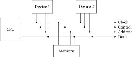
Figure 4.3 Organization of a bus.
Bus master
In a typical bus system, the CPU serves as the bus master and initiates all transfers. If any device could request a transfer, then other devices might be starved of bus bandwidth. As bus master, the CPU reads and writes data and instructions from memory. It also initiates all reads or writes on I/O devices. We will see shortly that DMA allows other devices to temporarily become the bus master and transfer data without the CPU’s involvement.
Four-cycle handshake
The basic building block of most bus protocols is the four-cycle handshake, illustrated in Figure 4.4. The handshake ensures that when two devices want to communicate, one is ready to transmit and the other is ready to receive. The handshake uses a pair of wires dedicated to the handshake: enq (meaning enquiry) and ack (meaning acknowledge). Extra wires are used for the data transmitted during the handshake. Each step in the handshake is identified by a transition on enq or ack:
1. Device 1 raises its output to signal an enquiry, which tells device 2 that it should get ready to listen for data.
2. When device 2 is ready to receive, it raises its output to signal an acknowledgment. At this point, devices 1 and 2 can transmit or receive.
3. Once the data transfer is complete, device 2 lowers its output, signaling that it has received the data.
4. After seeing that ack has been released, device 1 lowers its output.
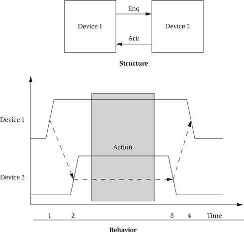
Figure 4.4 The four-cycle handshake.
At the end of the handshake, both handshaking signals are low, just as they were at the start of the handshake. The system has thus returned to its original state in readiness for another handshake-enabled data transfer.
Bus signals
Microprocessor buses build on the handshake for communication between the CPU and other system components. The term bus is used in two ways. The most basic use is as a set of related wires, such as address wires. However, the term may also mean a protocol for communicating between components. To avoid confusion, we will use the term bundle to refer to a set of related signals. The fundamental bus operations are reading and writing. The major components on a typical bus include:
• Clock provides synchronization to the bus components;
• R/W’ is true when the bus is reading and false when the bus is writing;
• Address is an a-bit bundle of signals that transmits the address for an access;
• Data is an n-bit bundle of signals that can carry data to or from the CPU; and
• Data ready signals when the values on the data bundle are valid.
All transfers on this basic bus are controlled by the CPU—the CPU can read or write a device or memory, but devices or memory cannot initiate a transfer. This is reflected by the fact that R/W’ and address are unidirectional signals, because only the CPU can determine the address and direction of the transfer.
Bus reads and writes
Figure 4.5 shows a sequence diagram for a read followed by a write. The CPU first reads a location from memory and then writes it to dev1. The bus mediates each transfer. The bus operates under a protocol that determines when components on the bus can use certain signals and what those signals mean. The details of bus protocols are not important here. But it is important to keep in mind that bus operations take time; the clock frequency of the bus is often much lower than that of the CPU. We will see how to analyze platform-level performance in Section 4.7.
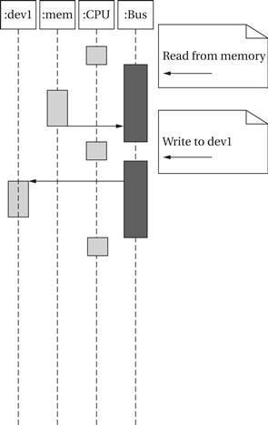
Figure 4.5 A typical sequence diagram for bus operations.
Sequence diagrams don’t give us enough detail to fully understand the hardware. To provide the required detail, the behavior of a bus is most often specified as a timing diagram. A timing diagram shows how the signals on a bus vary over time, but because values like the address and data can take on many values, some standard notation is used to describe signals, as shown in Figure 4.6. A’s value is known at all times, so it is shown as a standard waveform that changes between zero and one. B and C alternate between changing and stable states. A stable signal has, as the name implies, a stable value that could be measured by an oscilloscope, but the exact value of that signal does not matter for purposes of the timing diagram. For example, an address bus may be shown as stable when the address is present, but the bus’s timing requirements are independent of the exact address on the bus. A signal can go between a known 0/1 state and a stable/changing state. A changing signal does not have a stable value. Changing signals should not be used for computation. To be sure that signals go to their proper values at the proper times, timing diagrams sometimes show timing constraints. We draw timing constraints in two different ways, depending on whether we are concerned with the amount of time between events or only the order of events. The timing constraint from A to B, for example, shows that A must go high before B becomes stable. The constraint from A to B also has a time value of 10 ns, indicating that A goes high at least 10 ns before B goes stable.
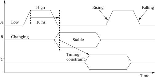
Figure 4.6 Timing diagram notation.
Figure 4.7 shows a timing diagram for the example bus. The diagram shows a read followed by a write. Timing constraints are shown only for the read operation, but similar constraints apply to the write operation. The bus is normally in the read mode because that does not change the state of any of the devices or memories. The CPU can then ignore the bus data lines until it wants to use the results of a read. Notice also that the direction of data transfer on bidirectional lines is not specified in the timing diagram. During a read, the external device or memory is sending a value on the data lines, while during a write the CPU is controlling the data lines.
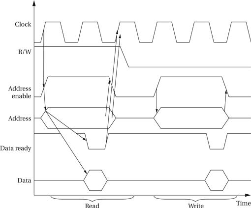
Figure 4.7 Timing diagram for read and write on the example bus.
With practice, we can see the sequence of operations for a read on the timing diagram:
• A read or write is initiated by setting address enable high after the clock starts to rise. We set R/W = 1 to indicate a read, and the address lines are set to the desired address.
• One clock cycle later, the memory or device is expected to assert the data value at that address on the data lines. Simultaneously, the external device specifies that the data are valid by pulling down the data ready line. This line is active low, meaning that a logically true value is indicated by a low voltage, in order to provide increased immunity to electrical noise.
• The CPU is free to remove the address at the end of the clock cycle and must do so before the beginning of the next cycle. The external device has a similar requirement for removing the data value from the data lines.
The write operation has a similar timing structure. The read/write sequence illustrates that timing constraints are required on the transition of the R/W signal between read and write states. The signal must, of course, remain stable within a read or write. As a result there is a restricted time window in which the CPU can change between read and write modes.
The handshake that tells the CPU and devices when data are to be transferred is formed by data ready for the acknowledge side, but is implicit for the enquiry side. Because the bus is normally in read mode, enq does not need to be asserted, but the acknowledge must be provided by data ready.
The data ready signal allows the bus to be connected to devices that are slower than the bus. As shown in Figure 4.8, the external device need not immediately assert data ready. The cycles between the minimum time at which data can be asserted and when it is actually asserted are known as wait states. Wait states are commonly used to connect slow, inexpensive memories to buses.
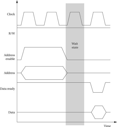
Figure 4.8 A wait state on a read operation.
We can also use the bus handshaking signals to perform burst transfers, as illustrated in Figure 4.9. In this burst read transaction, the CPU sends one address but receives a sequence of data values. We add an extra line to the bus, called burst’ here, which signals when a transaction is actually a burst. Releasing the burst’ signal tells the device that enough data has been transmitted. To stop receiving data after the end of data 4, the CPU releases the burst’ signal at the end of data 3 because the device requires some time to recognize the end of the burst. Those values come from successive memory locations starting at the given address.
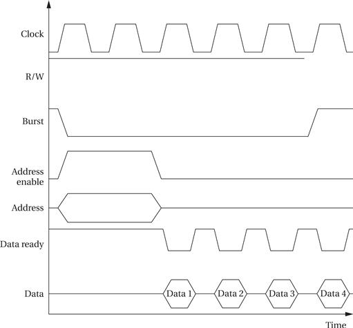
Figure 4.9 A burst read transaction.
Some buses provide disconnected transfers. In these buses, the request and response are separate. A first operation requests the transfer. The bus can then be used for other operations. The transfer is completed later, when the data are ready.
The state machine view of the bus transaction is also helpful and a useful complement to the timing diagram. Figure 4.10 shows the CPU and device state machines for the read operation. As with a timing diagram, we do not show all the possible values of address and data lines but instead concentrate on the transitions of control signals. When the CPU decides to perform a read transaction, it moves to a new state, sending bus signals that cause the device to behave appropriately. The device’s state transition graph captures its side of the protocol.
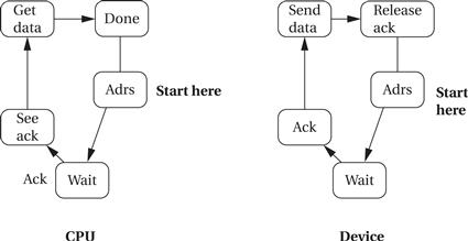
Figure 4.10 State diagrams for the bus read transaction.
Some buses have data bundles that are smaller than the natural word size of the CPU. Using fewer data lines reduces the cost of the chip. Such buses are easiest to design when the CPU is natively addressable. A more complicated protocol hides the smaller data sizes from the instruction execution unit in the CPU. Byte addresses are sequentially sent over the bus, receiving one byte at a time; the bytes are assembled inside the CPU’s bus logic before being presented to the CPU proper.
4.3.2 DMA
Standard bus transactions require the CPU to be in the middle of every read and write transaction. However, there are certain types of data transfers in which the CPU does not need to be involved. For example, a high-speed I/O device may want to transfer a block of data into memory. While it is possible to write a program that alternately reads the device and writes to memory, it would be faster to eliminate the CPU’s involvement and let the device and memory communicate directly. This capability requires that some unit other than the CPU be able to control operations on the bus.
Direct memory access (DMA) is a bus operation that allows reads and writes not controlled by the CPU. A DMA transfer is controlled by a DMA controller, which requests control of the bus from the CPU. After gaining control, the DMA controller performs read and write operations directly between devices and memory.
Figure 4.11 shows the configuration of a bus with a DMA controller. The DMA requires the CPU to provide two additional bus signals:
• The bus request is an input to the CPU through which DMA controllers ask for ownership of the bus.
• The bus grant signals that the bus has been granted to the DMA controller.
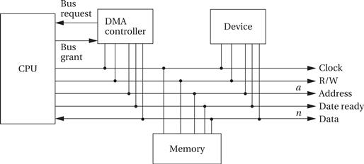
Figure 4.11 A bus with a DMA controller.
The DMA controller can act as a bus master. It uses the bus request and bus grant signal to gain control of the bus using a classic four-cycle handshake. A bus request is asserted by the DMA controller when it wants to control the bus, and the bus grant is asserted by the CPU when the bus is ready. The CPU will finish all pending bus transactions before granting control of the bus to the DMA controller. When it does grant control, it stops driving the other bus signals: R/W, address, and so on. Upon becoming bus master, the DMA controller has control of all bus signals (except, of course, for bus request and bus grant).
Once the DMA controller is bus master, it can perform reads and writes using the same bus protocol as with any CPU-driven bus transaction. Memory and devices do not know whether a read or write is performed by the CPU or by a DMA controller. After the transaction is finished, the DMA controller returns the bus to the CPU by deasserting the bus request, causing the CPU to de-assert the bus grant.
The CPU controls the DMA operation through registers in the DMA controller. A typical DMA controller includes the following three registers:
• A starting address register specifies where the transfer is to begin.
• A length register specifies the number of words to be transferred.
• A status register allows the DMA controller to be operated by the CPU.
The CPU initiates a DMA transfer by setting the starting address and length registers appropriately and then writing the status register to set its start transfer bit. After the DMA operation is complete, the DMA controller interrupts the CPU to tell it that the transfer is done.
Concurrency during DMA
What is the CPU doing during a DMA transfer? It cannot use the bus. As illustrated in Figure 4.12, if the CPU has enough instructions and data in the cache and registers, it may be able to continue doing useful work for quite some time and may not notice the DMA transfer. But once the CPU needs the bus, it stalls until the DMA controller returns bus mastership to the CPU.
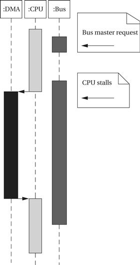
Figure 4.12 UML sequence of system activity around a DMA transfer.
To prevent the CPU from idling for too long, most DMA controllers implement modes that occupy the bus for only a few cycles at a time. For example, the transfer may be made 4, 8, or 16 words at a time. As illustrated in Figure 4.13, after each block, the DMA controller returns control of the bus to the CPU and goes to sleep for a preset period, after which it requests the bus again for the next block transfer.
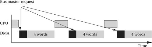
Figure 4.13 Cyclic scheduling of a DMA request.
4.3.3 System Bus Configurations
A microprocessor system often has more than one bus. As shown in Figure 4.14, high-speed devices may be connected to a high-performance bus, while lower-speed devices are connected to a different bus. A small block of logic known as a bridge allows the buses to connect to each other. There are three reasons to do this:
• Higher-speed buses may provide wider data connections.
• A high-speed bus usually requires more expensive circuits and connectors. The cost of low-speed devices can be held down by using a lower-speed, lower-cost bus.
• The bridge may allow the buses to operate independently, thereby providing some parallelism in I/O operations.
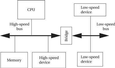
Figure 4.14 A multiple bus system.
Bus bridges
Let’s consider the operation of a bus bridge between what we will call a fast bus and a slow bus as illustrated in Figure 4.15. The bridge is a slave on the fast bus and the master of the slow bus. The bridge takes commands from the fast bus on which it is a slave and issues those commands on the slow bus. It also returns the results from the slow bus to the fast bus—for example, it returns the results of a read on the slow bus to the fast bus.
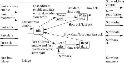
Figure 4.15 UML state diagram of bus bridge operation.
The upper sequence of states handles a write from the fast bus to the slow bus. These states must read the data from the fast bus and set up the handshake for the slow bus. Operations on the fast and slow sides of the bus bridge should be overlapped as much as possible to reduce the latency of bus-to-bus transfers. Similarly, the bottom sequence of states reads from the slow bus and writes the data to the fast bus.
The bridge serves as a protocol translator between the two bridges as well. If the bridges are very close in protocol operation and speed, a simple state machine may be enough. If there are larger differences in the protocol and timing between the two buses, the bridge may need to use registers to hold some data values temporarily.
ARM bus
Because the ARM CPU is manufactured by many different vendors, the bus provided off-chip can vary from chip to chip. ARM has created a separate bus specification for single-chip systems. The AMBA bus [ARM99A] supports CPUs, memories, and peripherals integrated in a system-on-silicon. As shown in Figure 4.16, the AMBA specification includes two buses. The AMBA high-performance bus (AHB) is optimized for high-speed transfers and is directly connected to the CPU. It supports several high-performance features: pipelining, burst transfers, split transactions, and multiple bus masters.
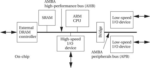
Figure 4.16 Elements of the ARM AMBA bus system.
A bridge can be used to connect the AHB to an AMBA peripherals bus (APB). This bus is designed to be simple and easy to implement; it also consumes relatively little power. The APB assumes that all peripherals act as slaves, simplifying the logic required in both the peripherals and the bus controller. It also does not perform pipelined operations, which simplifies the bus logic.