
Single phase series a.c. circuits
Publisher Summary
This chapter discusses the single phase series alternating current (a.c.) circuits. The voltage magnification at resonance is the ratio measured of the quality of a circuit—as a resonator or tuning device—and is called the Q-factor. The advantages of a high Q-factor in a series high frequency circuit is that such circuits need to be selective to signals at the resonant frequency and must be less selective to other frequencies. The disadvantage of a high Q-factor in a series power circuit is that it can lead to dangerously high voltages across the insulation and may lead to electrical breakdown. For series-connected impedances, the total circuit impedance can be represented as a single L–C–R circuit by combining all values of resistance together, all values of inductance together and all values of capacitance together.
1. In a purely resistive a.c. circuit, the current IR and applied voltage VR are in phase, see Figure 13.1(a).
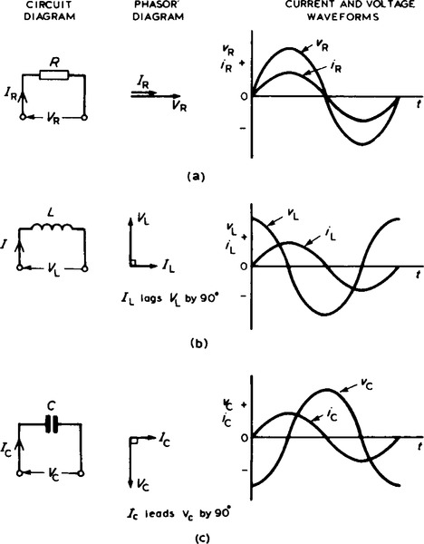
2. In a purely inductive a.c. circuit, the current IL lags the applied voltage VL by 90° (i.e. π/2 rads), see Figure 13.1(b).
3. In a purely capacitive a.c. circuit, the current IC leads the applied voltage VC by 90° (i.e. π/2 rads), see Figure 13.1(c).
4. In a purely inductive circuit the opposition to the flow of alternating current is called the inductive reactance, XL.
where f is the supply frequency in hertz and L is the inductance in henry’s.
XL, is proportional to f as shown in Figure 13.2(a).
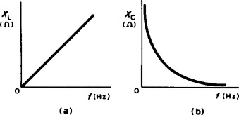
5. In a purely capacitive circuit the opposition to the flow of alternating current is called the capacitive reactance, XC.
where C is the capacitance in farads. XC varies with f as shown in Figure 13.2(b).
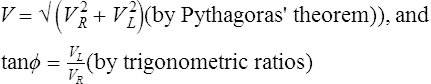
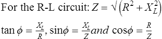
6. In an a.c. series circuit containing inductance L and resistance R, the applied voltage V is the phasor sum of VR and VL (see Figure 13.3(a)) and thus the current I lags the applied voltage V by an angle lying between 0° and 90° (depending on the values of VR and VL), shown as angle ϕ. In any a.c. series circuit the current is common to each component and is thus taken as the reference phasor.
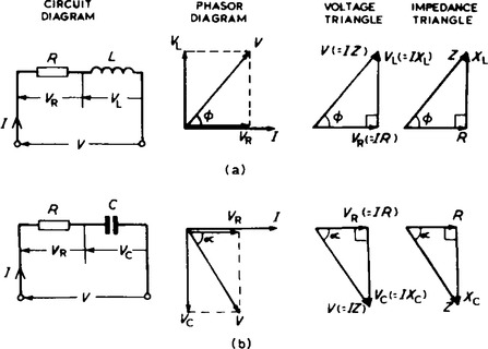
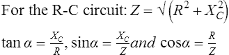
7. In an a.c. series circuit containing capacitance C and resistance R, the applied voltage V is the phasor sum of VR and VC (see Figure 13.3(b)) and thus the current I leads the applied voltage V by an angle lying between 0° and 90° (depending on the values of VR and VC), shown as angle α.
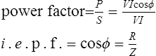
8. In an a.c. circuit, the ratio
9. From the phasor diagrams of Figure 13.3, the ‘voltage triangles’ are derived.
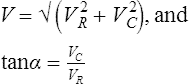
10. If each side of the voltage triangles in Figure 13.3 is divided by current I then the ‘impedance triangles’ are derived.
11. In an a.c. series circuit containing resistance R, inductance L and capacitance C, the applied voltage V is the phasor sum of VR, VL and VC (see Figure 13.4). VL, and VC are anti-phase and there are three phasor diagrams possible — each depending on the relative values of VL and VC.
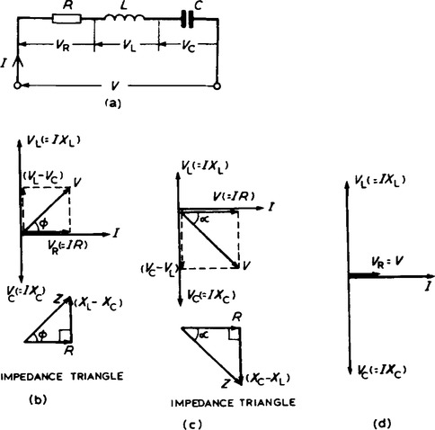
12. When XL>XC (see Figure 13.4(b)):
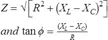
13. When XC>XL (see Figure 13.4(c)):
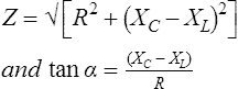
14. When XL = XC (see Figure 13.4(d)), the applied voltage V and the current I are in phase. This effect is called series resonance. At resonance:
(ii) Z=R (i.e. the minimum circuit impedance possible in an L-C-R circuit).
(iii) I =![]() (i.e. the maximum current possible in an L-C-R circuit).
(i.e. the maximum current possible in an L-C-R circuit).
(iv) Since XL = XC, then ![]() , from which,
, from which, ![]() Hz, where fr, is the resonant frequency.
Hz, where fr, is the resonant frequency.
15. At resonance, if R is small compared with XL, and XC, it is possible for VL and VC to have voltages many times greater than the supply voltage V (see Figure 13.4(d)).
This ratio is a measure of the quality of a circuit (as a resonator or tuning device) and is called the Q-factor.
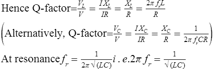
(a) The advantages of a high Q-factor in a series high frequency circuit is that such circuits need to be ‘selective’ to signals at the resonant frequency and must be less selective to other frequencies.
(b) The disadvantage of a high Q-factor in a series power circuit is that it can lead to dangerously high voltages across the insulation and may lead to electrical breakdown.
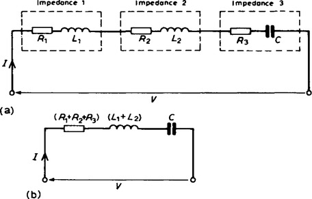
17. For series-connected impedances the total circuit impedance can be represented as a single L-C-R circuit by combining all values of resistance together, all values of inductance together and all values of capacitance together (remembering that for series connected capacitors 1/C = 1/C1 + 1/C2 + ···). For example, the circuit of Figure 13.5(a) showing three impedances has an equivalent circuit of Figure 13.5(b).
(a) For a purely resistive a.c. circuit, the average power dissipated, P, is given by: P = VI = I2R = V2/R watts (V and I being r.m.s. values). See Figure 13.6(a).
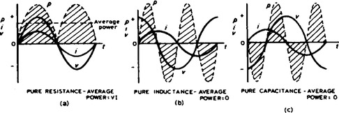
(b) For a purely inductive a.c. circuit, the average power is zero. See Figure 13.6(b).
(c) For a purely capacitive a.c. circuit, the average power is zero. See Figure 13.6(c).
In Figure 13.6(a)-(c), the value of power at any instant is given by the product of the voltage and current at that instant, i.e. the instantaneous power, p = vi, as shown by the broken lines.
19. Figure 13.7 shows current and voltage waveforms for an R-L circuit where the current lags the voltage by angle ϕ. The waveform for power (where p = vi) is shown by the broken line, and its shape, and hence average power, depends on the value of angle ϕ.
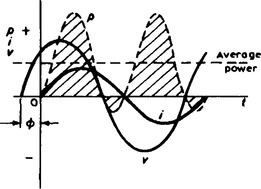
For an R-L, R-C or L-C-R series a.c. circuit, the average power P is given by:
P = VI cos ϕ watts or P = I2R watts (V and I being r.m.s. values).
20. Figure 13.8(a) shows a phasor diagram in which the current I lags the applied voltage V by angle ϕ. The horizontal component of V is V cos ϕ and the vertical component of V is V sin ϕ. If each of the voltage phasors is multiplied by I, Figure 13.8(b) is obtained and is known as the ‘power triangle’.
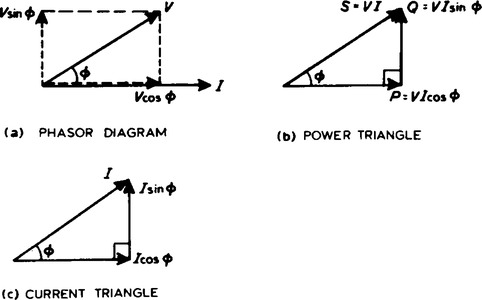
Apparent power, S = VI voltamperes (VA)
True or active power, P = VI cos ϕ watts (W)
Reactive power, Q = VI sin ϕ reactive voltamperes (VAr)
21. If each of phasors of the power triangle of Figure 13.8(b) is divided by V, Figure 13.8(c) is obtained and is known as the ‘current triangle’. The horizontal component of current, I cos ϕ, is called the active or the in-phase component. The vertical component of current, I sin ϕ, is called the reactive or the quadrature component.
For sinusoidal voltages and currents,
(from Figure 13.3).
(The relationships stated in paras 20 to 22 are also true when current I leads voltage V.)