
Semiconductor diodes
Publisher Summary
This chapter focuses on semiconductor diodes. Materials may be classified as conductors, semiconductors or insulators. The classification depends on the value of resistivity of the material. The most important semiconductors used in the electronics industry are silicon and germanium. As the temperature of these materials is raised above room temperature, the resistivity is reduced and ultimately a point is reached where they effectively become conductors. For this reason, silicon should not operate at a working temperature in excess of 150°C–200°C, depending on its purity, and germanium should not operate at a working temperature in excess of 75°C–90°C, depending on its purity. A semiconductor diode is a device having a p–n junction mounted in a container, suitable for conducting and dissipating the heat generated in operation and having connecting leads.
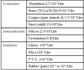
1. Materials may be classified as conductors, semiconductors or insulators. The classification depends on the value of resistivity of the material. Good conductors are usually metals and have resistivities in the order of 10−7 to 10−8 ohm metres.
Semiconductors have resistivities in the order of 10−3 to 3 × 10⁸ The resistivities of insulators are in the order of 104 to 1014 Ω. Some typical approximate values at normal room temperatures are:
| Conductors: | Aluminium 2.7×10⁻⁸Ωm |
| Brass (70 Cu/30 Zn) 8×10⁻⁸Ωm | |
| Copper (pure anneal; d) 1.7×10⁻⁸Ωm | |
| Steel (mild) 15×108Ωm | |
| Semiconductors. | Silicon 2.3×10³Ωm |
| Germanium 0.45Ωm | |
| Insulators: | Glassy ≥1010Ωm |
| Mica ≥1011Ωm | |
| P.V.C. ≥1013Ωm | |
| Rubber (pure) 1012 to 1014Ωm |
2. In general, over a limited range of temperatures, the resistance of a conductor increases with temperature increase. The resistance of insulators remains approximately constant with variation of temperature. The resistance of semiconductor materials decreases as the temperature increases. For a specimen of each of these materials, having the same resistance (and thus completely different dimensions), at, say, 15°C, the variation for a small increase in temperature to t°C is as shown in Figure 16.1.

3. The most important semiconductors used in the electronics industry are silicon and germanium. As the temperature of these materials is raised above room temperature, the resistivity is reduced and ultimately a point is reached where they effectively become conductors. For this reason, silicon should not operate at a working temperature in excess of 150°C to 200°C, depending on its purity, and germanium should not operate at a working temperature in excess of 75°C to 90°C, depending on its purity. As the temperature of a semiconductor is reduced below normal room temperature, the resistivity increases until, at very low temperatures, the semiconductor becomes an insulator.
4. Adding extremely small amounts of impurities to pure semiconductors in a controlled manner is called doping. Antimony, arsenic and phosphorus are called n-type impurities and form an n-type material when any of these impurities are added to silicon or germanium. The amount of impurity added usually varies from 1 part impurity in 108 parts semiconductor material to 1 part impurity to 106 parts semiconductor material, depending on the resistivity required. Indium, aluminium and boron are called p-type impurities and form a p-type material when any of these impurities are added to a semiconductor.
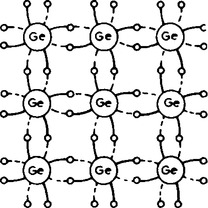
5. In semiconductor materials, there are very few charge carriers per unit volume free to conduct. This is because the ‘four electron structure’ in the outer shell of the atoms (called valency electrons), form strong covalent bonds with neighbouring atoms, resulting in a tetrahedral structure with the electrons held fairly rigidly in place. A two-dimensional diagram depicting this is shown for germanium in Figure 16.2.
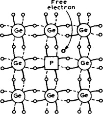
Arsenic, antimony and phosphorus have five valency electrons and when a semiconductor is doped with one of these substances, some impurity atoms are incorporated in the tetrahedral structure. The ‘fifth’ valency electron is not rigidly bonded and is free to conduct, the impurity atom donating a charge carrier. A two-dimensional diagram depicting this is shown in Figure 16.3, in which a phosphorus atom has replaced one of the germanium atoms. The resulting material is called n-type material, and contains free electrons.
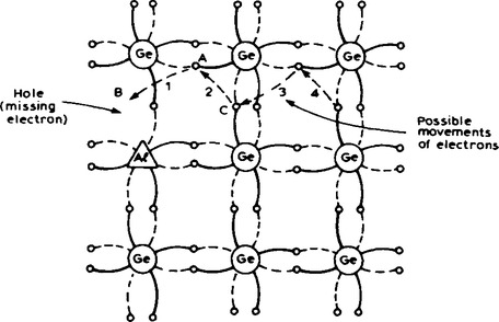
Indium, aluminium and boron have three valency electrons and when a semiconductor is doped with one of these substances, some of the semiconductor atoms are replaced by impurity atoms. One of the four bonds associated with the semiconductor material is deficient by one electron and this deficiency is called a hole. Holes give rise to conduction when a potential difference exists across the semiconductor material due to movement of electrons from one hole to another, as shown in Figure 16.4. In this figure, an electron moves from A to B, giving the appearance that the hole moves from B to A. Then electron C moves to A, giving the appearance that the hole moves to C, and so on. The resulting material is p-type material containing holes.
6. A p-n junction is a piece of semiconductor material in which part of the material is p-type and part is n-type. In order to examine the charge situation, assume that separate blocks of p-type and n-type materials are pushed together. Also assume that a hole is a positive charge carrier and that an electron is a negative charge carrier. At the junction, the donated electrons in the n-type material, called majority carriers, diffuse into the p-type material (diffusion is from an area of high density to an area of lower density.) and the acceptor holes in the p-type material diffuse into the n-type material as shown by the arrows in Figure 16.5.
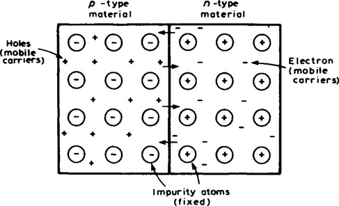
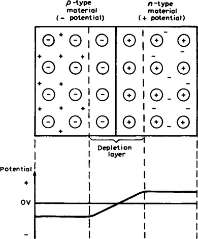
Because the n-type material has lost electrons, it acquires a positive potential with respect to the p-type material and thus tends to prevent further movement of electrons. The p-type material has gained electrons and becomes negatively charged with respect to the n-type material and hence tends to retain holes. Thus after a short while, the movement of electrons and holes stops due to the potential difference across the junction, called the contact potential. The area in the region of the junction becomes depleted of holes and electrons due to electron-hole recombinations, and is called a depletion layer, as shown in Figure 16.6.
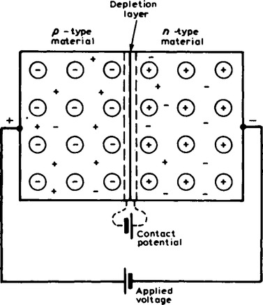
7. When an external voltage is applied to a p-n junction making the p-type material positive with respect to the n-type material, as shown in Figure 16.7, the p-n junction is forward biased. The applied voltage opposes the contact potential, and, in effect, closes the depletion layer. Holes and electrons can now cross the junction and a current flows. An increase in the applied voltage above that required to narrow the depletion layer (about 0.2 V for germanium and 0.6 V for silicon), results in a rapid rise in the current flow. Graphs depicting the current-voltage relationship for forward biased p-n junctions, for both germanium and silicon, called the forward characteristics, are shown in Figure 16.8.

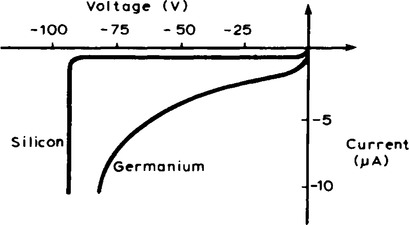
When an external voltage is applied to a p-n junction making the p-type material negative with respect to the n-type material, as shown in Figure 16.9, the p-n junction is reverse biased. The applied voltage is now in the same sense as the contact potential and opposes the movement of holes and electrons, due to opening up the depletion layer. Thus, in theory, no current flows. However, at normal room temperature, certain electrons in the covalent bond lattice acquire sufficient energy from the heat available to leave the lattice, generating mobile electrons and holes. This process is called electron-hole generation by thermal excitation.

The electrons in the p-type material and holes in the n-type material caused by thermal excitation, are called minority carriers and these will he attracted by the applied voltage. Thus, in practice, a small current of a few micro-amperes for germanium and less than one micro-ampere for silicon, at normal room
temperature, flows under reverse bias conditions. Typical reverse charcteristics are shown in Figure 16.10 for both germanium and silicon.
8. A semiconductor diode is a device having a p-n junction mounted in a container, suitable for conducting and dissipating the heat generated in operation and having connecting leads. Its operating characteristics are as shown in Figure 16.8 and Figure 16.10. Two circuit symbols for semiconductor diodes are in common use and are shown in Figure 16.11.
