
Transistors
Publisher Summary
This chapter discusses transistors and their several types. The bipolar junction transistor consists of three regions of semiconductor material. One type is called a p–n–p transistor, in which two regions of p-type material sandwich a thin layer of n-type material. A second type is called an n–p–n transistor, in which two regions of n-type material sandwich a thin layer of p-type material. Both of these types of transistors consist of two p–n junctions placed close to one another in a back-to-back arrangement on a single piece of semiconductor material. Transistors have three connecting leads and in operation an electrical input to one pair of connections, say the emitter and base connections can control the output from another pair, say the collector and emitter connections. This type of operation is achieved by appropriately biasing the two internal p–n junctions.
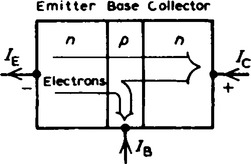
1. The bipolar junction transistor consists of three regions of semiconductor material. One type is called a p-n-p transistor, in which two regions of p-type material sandwich a very thin layer of n-type material. A second type is called a n-p-n transistor, in which two regions of n-type material sandwich a very thin layer of p-type material. Both of these types of transistors consist of two p-n junctions placed very close to one another in a back-to-back arrangement on a single piece of semiconductor material. Diagrams depicting these two types of transistor are shown in Figure 17.1.
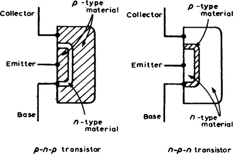
The two p-type material regions of the p-n-p transistor are called the emitter and collector and the n-type material is called the base. Similarly, the two n-type material regions of the n-p-n transistor are called the emitter and collector and the p-type material region is called the base, as shown in Figure 17.1.
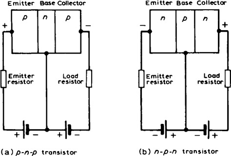
2. Transistors have three connecting leads and in operation an electrical input to one pair of connections, say the emitter and base connections can control the output from another pair, say the collector and emitter connections. This type of operation is achieved by appropriately biasing the two internal p-n junctions. When batteries and resistors are connected to a p-n-p transistor, as shown in Figure 17.2(a), the base-emitter junction is forward biased and the base-collector junction is reverse biased. Similarly, an n-p-n transistor has its base-emitter junction forward biased and its base-collector junction reverse biased when the batteries are connected as shown in Figure 17.2(b).
3. For a silicon p-n-p transistor, biased as shown in Figure 17.2(a), if the base-emitter junction is considered on its own, it is forward biased and a current flows. This is depicted in Figure 17.3(a). For example, if RE is 1000Ω, the battery is 4.5 V and the voltage drop across the junction is taken as 0.7 V, the current flowing is given by (4.5–0.7)/1000 = 3.8 mA. When the base-collector junction is considered on its own, as shown in Figure 17.3(b), it is reverse biased and the collector current is something less than one microampere.
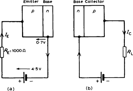
However, when both external circuits are connected to the transistor, most of the 3.8 mA of current flowing in the emitter, which previously flowed from the base connection, now flows out through the collector connection due to transistor action.
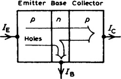
4. In a p-n-p transistor, connected as shown in Figure 17.2(a), transistor action is accounted for as follows:
(a) The majority carriers in the emitter p-type material are holes.
(b) The base-emitter junction is forward biased to the majority carriers and the holes cross the junction and appear in the base region.
(c) The base region is very thin and is only lightly doped with electrons so although some electron-hole pairs are formed, many holes are left in the base region.
(d) The base-collector junction is reverse biased to electrons in the base region and holes in the collector region, but forward biased to holes in the base region. These holes are attracted by the negative potential at the collector terminal.
(e) A large proportion of the holes in the base region cross the base-collector junction into the collector region, creating a collector current. Conventional current flow is in the direction of hole movement.
The transistor action is shown diagrammatically in Figure 17.4.
For transistors having very thin base regions, up to ![]() of the holes leaving the emitter cross the base collector junction.
of the holes leaving the emitter cross the base collector junction.
5. In an n-p-n transistor, connected as shown in Figure 17.2(b), transistor action is accounted for as follows:
(a) The majority carriers in the n-type emitter material are electrons.
(b) The base-emitter junction is forward biased to these majority carriers and electrons cross the junction and appear in the base region.
(c) The base region is very thin and only lightly doped with holes, so some recombination with holes occurs but many electrons are left in the base region.
(d) The base-collector junction is reverse biased to holes in the base region and electrons in the collector region, but is forward biased to electrons in the base region. These electrons are attracted by the positive potential at the collector terminal.
(e) A large proportion of the electrons in the base region cross the base-collector junction into the collector region, creating a collector current.
The transistor action is shown diagrammatically in Figure 17.5. As stated in para. 4, conventional current flow is taken to be in the direction of hole flow, that is, in the opposite direction to electron flow, hence the directions of the conventional current flow are as shown in Figure 17.5.
6. For a p-n-p transistor, the base-collector junction is reverse biased for majority carriers. However, a small leakage current, ICBO flows from the base to the collector due to thermally generated minority carriers (electrons in the collector and holes in the base), being present.
The base-collector junction is forward biased to these minority carriers. If a proportion, α, (having a value of up to 0.995 in modern transistors), of the holes passing into the base from the emitter, pass through the base-collector junction, then the various currents flowing in a p-n-p transistor are as shown in Figure 17.6.
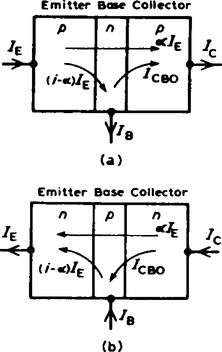
Similarly, for a n-p-n transistor, the base-collector junction is reverse biased for majority carriers, but a small leakage current, ICBO, flows from the collector to the base due to thermally generated minority carriers (holes in the collector and electrons in the base), being present. The base-collector junction is forward biased to these minority carriers. If a proportion, α, of the electrons passing through the base-emitter junction also pass through the base-collector junction, then the currents flowing in an n-p-n transistor are as shown in Figure 17.6.
7. Symbols are used to represent p-n-p and n-p-n transistors in circuit diagrams and two of these in common use are shown in Figure 17.7. The arrow head drawn on the emitter of the symbol is in the direction of conventional emitter current (hole flow). The potentials marked at the collector, base and emitter are typical values for a silicon transistor having a potential difference of 6 V between its collector and its emitter.
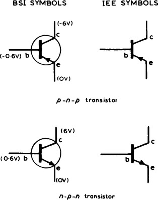
The voltage of 0.6 V across the base and emitter is that required to reduce the potential barrier and if it is raised slightly to, say, 0.62 V, it is likely that the collector current will double to about 2 mA. Thus a small change of voltage between the emitter and the base can give a relatively large change of current in the emitter circuit. Because of this, transistors can be used as amplifiers.
8. There are three ways of connecting a transistor, depending on the use to which it is being put. The ways are classified by the electrode which is common to both the input and the output.
(a) common-base configuration, shown in Figure 17.8(a),
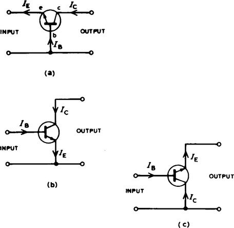
(b) common-emitter configuration, shown in Figure 17.8(b), and
(c) common-collector configuration, shown in Figure 17.8(c).
These configurations are for an n-p-n transistor. The current flows shown are all reversed for a p-n-p transistor.
9. The effect of changing one or more of the various voltages and currents associated with a transistor circuit can be shown graphically and these graphs are called the characteristics of the transistor. As there are five variables (collector, base and emitter currents and voltages across the collector and base and emitter and base) and also three configurations, many characteristics are possible. Some of the possible characteristics are given below.
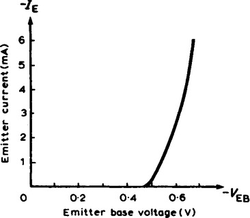
(i) Input characteristic. With reference to Figure 17.8(a), the input to a common-base transistor is the emitter current, IE, and can be varied by altering the base-emitter voltage VEB. The base-emitter junction is essentially a forward biased junction diode, so as VEB is varied, the current flowing is similar to that for a junction diode, as shown in Figure 17.9 for a silicon transistor. Figure 17.9 is called the input characteristic for an n-p-n transistor having common-base configuration. The variation of the collector-base voltage VCB has little effect on the characteristic. A similar characteristic can be obtained for a p-n-p transistor, these having reversed polarities.
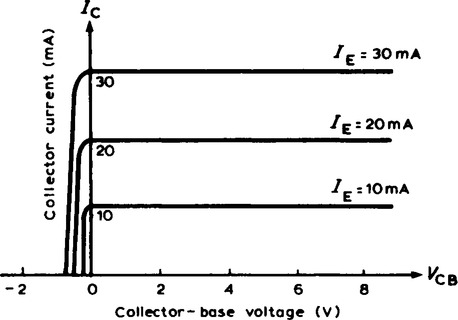
(ii) Output characteristics The value of the collector current IC is very largely determined by the emitter current, IE. For a given value of IE, the collector-base voltage, VCB, can be varied and has little effect on the value of IC. If VCB is made slightly negative, the collector no longer attracts the majority carriers leaving the emitter and IC falls rapidly to zero. A family of curves for various values of IE are possible and some of these are shown in Figure 17.10 Figure 17.10 is called the output characteristic from an n-p-n transistor having common-base configuration. Similar characteristics can be obtained for a p-n-p transistor, these having reversed polarities.
b. Common-emitter configuration
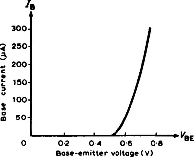
(i) Input characteristic In a common-emitter configuration (see Figure 17.8(b)) the base current is now the input current. As VEB is varied, the characteristic obtained is similar in shape to the input characteristic for a common-base configuration shown in Figure 17.9, but the values of current are far less. With reference to Figure 17.6(a), as long as the junction are biased as described, the three currents, IE, IC and IB keep the ratio 1:α : (1–α) whichever configuration is adopted.
Thus the base current changes are much smaller than the corresponding emitter current changes and the input characteristic for an n-p-n transistor is as shown in Figure 17.11. A similar characteristic can be obtained for a p-n-p transistor, these having reversed polarities.
(ii) Output characteristics A family of curves can be obtained depending on the value of base current IB and some of these for an n-p-n transistor are shown in Figure 17.12. A similar set of characteristics can be obtained for a p-n-p transistor, these having reversed polarities. These characteristics differ from the common-base output characteristics in the following ways:
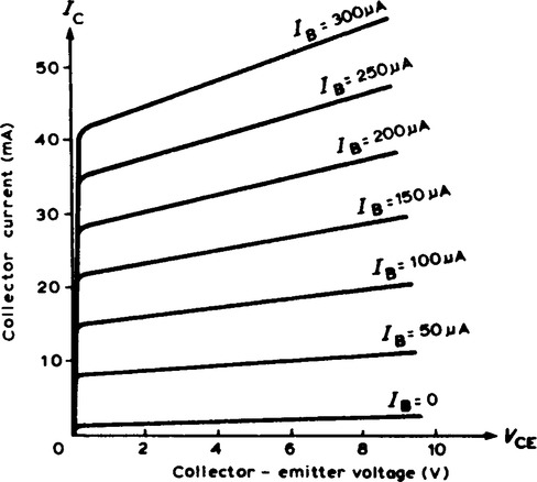
The collector current reduces to zero without having to reverse the collector voltage, and
The characteristics slope upwards indicating a lower output resistance (usually kilohms for a common-emitter configuration compared with megohms for a common-base configuration).