
]>
2
Electromagnetics of Simple Media: One-Dimensional Solution*
The mathematics needed to solve problems may be simplified if we are able to model the problem as one-dimensional. Sometimes a practical problem with the appropriate symmetries and dimensions will permit us to use one-dimensional models. A choice of the appropriate coordinate system will sometimes allow us to reduce the dimensionality of the problem. A few of such basic solutions will be listed next.
2.1Uniform Plane Waves in Sourceless Medium (ρV = 0, Jsource = 0)
A simple lossy medium with the parameters εr, μr, and σ has the following one-dimensional (say z-coordinate) solutions in Cartesian coordinates:
In the above, the braces {} indicate a linear combination of the functions within parentheses and Et is the electric field in the transverse (to z) plane. For a lossy medium,
and hence k is complex. The characteristic impedance η is given by
which is again complex. If k is written as (β − jα), then the phase factor exp(− jkz) = exp(−αz −jβz) gives the solution of an attenuated wave propagating in the positive z-direction. Here α is called the attenuation constant (Np/m) and β is called the phase constant (rad/m). Explicit expressions for α and β may be obtained by solving the two equations generated by equating the real and imaginary parts of the LHS with the RHS of Equation 2.4, respectively:
where
is called the loss tangent. For a low-loss dielectric, the loss tangent T ≪ 1 and
2.2Good Conductor Approximation
For the other limit of approximation, called the good-conductor approximation,
In the above, δ is called the skin depth. The characteristic impedance in this case is also called the surface impedance Zs:
2.3Uniform Plane Wave in a Good Conductor: Skin Effect
The attenuated positive-going wave in a good conductor is described by the phasor exp [−(1 + j)z/δ] and the real fields are of the form
where
From Equation 2.16, we see that the amplitude of the current density drops to e−1 (36.8%) of its value at a distance
In the case of direct current (DC), f = 0 and δ = ∞, indicating that the current density can be uniform. However, for the time-harmonic AC case (f ≠ 0), δ is finite, indicating that the current density is nonuniform and decays exponentially with distance. For example, at a distance of 4δ, the current density reduces (e−4 = 1.8%) practically to zero. In Table 2.1, we list the skin depth δ for a good conductor such as copper at various frequencies.
TABLE 2.1
Skin Depth for Copper
| f | 60 Hz | 1 kHz | 1 MHz | 10 GHz |
| δ | 1 cm | 2.45 mm | 7.75 × 10⁻² mm | 7.75 × 10⁻⁴ mm |
At high frequencies, the current is practically confined to the skin of the conductor and the phenomenon is hence described as a skin effect.
2.4Boundary Conditions at the Interface of a Perfect Electric Conductor with a Dielectric
We also note that δ = 0 for σ = ∞. That is the reason for the statement in Problem P2.1 that the time-harmonic fields in a perfect conductor are zero. If medium 1 is a perfect conductor and medium 2 is a dielectric, then the boundary conditions are
Thus, at the interface, the electric field is entirely normal to the interface and is equal to ρs/ε. Furthermore, the magnetic field is entirely tangential and is equal in magnitude to the surface current density K.
The PEC boundary condition
implies
where ˆt is a tangential unit vector and ˆn is a normal unit vector. Also the PEC boundary condition
implies
2.5AC Resistance
Figure 2.1 shows an infinitely deep good conductor of conductivity σ defined by the half-space 0 < x < ∞.
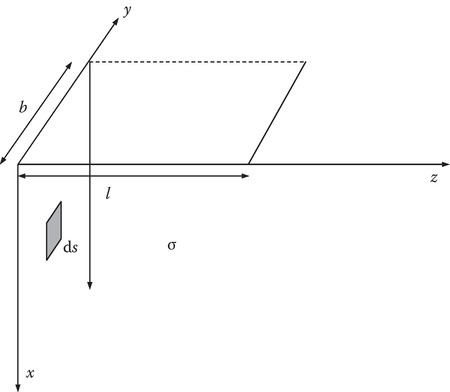
FIGURE 2.1
AC resistance of a semi-infinite good conductor.
The electric, magnetic, and current density phasors may be written as
and the corresponding real fields are
The time-averaged power density is given as
The total power entering the conductor of width b and length l is given by
The total phasor current entering the conductor of width b is given by
After integrating and substituting the limits, we obtain
Let us define RAC as an equivalent resistance that consumes the same power, that is,
From Equation 2.35, we obtain
From Equations 2.35 and 2.33, we obtain
Note that if the current were uniformly distributed (DC case), then we would have got the same resistance as given by Equation 2.38 if the depth of the conductor was δ. Figure 2.2 shows this equivalence.

FIGURE 2.2
Equivalent resistance.
2.6AC Resistance of Round Wires
The AC resistance of a round wire of radius a and length l is easily calculated for the two extreme cases of approximation δ ≫ a and δ ≪ a. For the former, the current may be considered as uniformly distributed and the DC resistance formula may be used:
For the latter, the analysis of the previous section may be applied. The circular conductor may be considered as a semi-infinite solid because δ ≪ a. Therefore, the effective area of cross-section seff (Figure 2.3) is given by
and
The analysis is more involved for the case where δ is comparable to a. In this case, we have to take a fresh look at the solution based on the one-dimensional solution in cylindrical coordinates (see Appendix 2A).
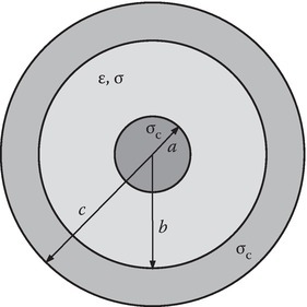
FIGURE 2.3
Cross section of a coaxial cable.
2.7Voltage and Current Harmonic Waves: Transmission Lines
A transmission line consists of two conductors that guide an electromagnetic wave from an electromagnetic source to an electromagnetic load. One approach to transmission line theory is through the distributed circuit theory. In this approach, we consider a differential length ∆z of a transmission line and describe its properties in terms of its per meter length circuit parameters, R′, the resistance due to imperfect conductors, L′, the inductance due to magnetic flux generated by the currents in the conductors, G′, the conductance due to an imperfect dielectric, and C′, the capacitance due to the surface charges on the conductors. We use electromagnetic theory to calculate the circuit parameters that depend on the electromagnetic properties of the materials used and their geometric arrangement. A parallel plate transmission line and a coaxial cable are two simple examples of transmission lines. Strip lines and microstrip lines are extensively used in high-frequency electromagnetic devices. Transmission line theory is often given in terms of voltage and current since in the transverse plane of a transmission line (cross section), the electromagnetic wave may be described as a TEM wave and the transverse fields satisfy the Laplace equation in the transverse plane. The voltage V and the current I can then be described as the appropriate integrals of the electric field and the magnetic field, respectively.
The parameters G′, L′, and C′ are computed as though the fields are static. For a coaxial cable (Figure 2.3), the parameters are given by [1]
The formulas to be used for the calculation of R′ and the corrections to L′ due to the internal inductance of the conductor will depend on the frequency. The previous section discussed the calculation of these parameters at high frequencies.
For high frequencies, that is, δ ≪ a,
and L′ including the correction due to the internal inductance (inductance due to the magnetic flux in the conductors) is given by
where
The parameters for other transmission lines may be calculated [1] using the same principles. After obtaining the parameters, the differential length transmission line may be represented as a two-port network shown in Figure 2.4 and expressed
which, in the limit ∆z approaches zero reduces to
Similar analysis for the current shows that
which, in the limit ∆z approaches zero reduces to
Equations 2.49 and 2.51 are the first-order coupled partial differential equations describing the voltage and current waves on a transmission line. The wave nature and the analogy with a simple electromagnetic wave may easily be seen by considering the following justifiable simplifications. As a first approximation, we can often neglect the losses in a transmission line and obtain the following wave equation for the voltage V(z, t):
where
If the source is harmonic, then
where
The solution may be written as
The superscript + is used for a positive-going wave and the superscript − is used for a negative-going wave. From Equation 2.49, the relationship between the voltages and the current may be obtained:
where
The following analogy with a TEM wave may be drawn:

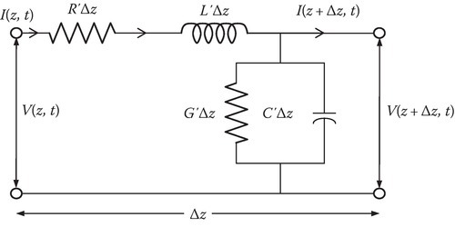
FIGURE 2.4
Circuit representation of a differential length of a transmission line.
Neglecting losses is equivalent to assumptions that the conductors are perfect (σc = ∞) and the dielectric is perfect (σ = 0). Practical lines have large but finite conductivity for conductors (e.g., copper σc = 5.7 × 10⁷ S/m) and small but nonzero conductivity for dielectrics (e.g., hard rubber, σ = 10−15 S/m). In such a case, R′ and G′ are nonzero and the propagation constant γ is
and the characteristic impedance Z0 is complex:
As expected, the solution to the transmission line equation is a linear combination of positive-going and negative-going attenuated traveling waves. Also, from the field viewpoint, we realize that the electromagnetic wave is no longer a pure TEM wave. To drive the current through the conductors, which are not perfect, a small Ez-component is needed. The integral of this component along the length of the conductors gives the voltage drop. The cross product of this z-component with the magnetic field H gives the power density. The time-averaged power density integrated over the surface of the conductor gives the power consumed by the conductors. Problem P2.5 is constructed to illustrate the approximate method of solving a transmission line problem and to understand the power flow in a transmission line.
2.8Bounded Transmission Line
Figure 2.5 shows a transmission line of length d with a load at z = 0, and a source of voltage Vg and internal impedance Zg connected at the point z = −d. From Equation 2.57 and Equation 2.58, the voltage at the terminals AB and the current ˜Ig=˜I(d) may be written as

FIGURE 2.5
Bounded transmission line.
The input impedance is given by
where Γ0 is the reflection coefficient at the load and is given by
By substituting Equation 2.66 into Equation 2.65, the input impedance may be written in an alternative form as
From Equation 2.67, several formulas for special lengths may be obtained
The circuit approximation applies if d≪λ=2πβ:
For a matched line, that is, ZL = Z0, Γ0 = 0, and
Equation 2.71 shows that for the matched line the length of the line has no effect on the input impedance, the right-going wave travels from the source to the load, there is no reflected wave, and the source wave is absorbed by the load. See Appendix 2B for power calculations.
A graphical method based on “Smith chart” is available to calculate the input impedance [1]. Appendix 2C gives the theory and application of the Smith chart.
The input impedance is reactive, if the load is either short-circuited or open-circuited and the reflection coefficient has a magnitude of 1:
In the above two cases, the waves are standing waves, there are permanent nulls in voltage at certain points on the transmission line, and the source does not supply any real power to the load but supplies only a reactive power.
Transmission line serves as a powerful analog for describing many electromagnetic phenomena since voltage and current variables are easily measurable and electrical engineers have a certain feel for these variables. Appendix 2B may be consulted for details of the transmission line theory. See Appendix 2C for application of the Smith chart to wave reflection problems.
The theory and applications of nonuniform transmission lines is given in Appendix 2D.
2.9Electromagnetic Wave Polarization
A plane wave solution given by Equation 2.1, Equation 2.2 and Equation 2.3 allows for x- and y-components of the electric and magnetic fields. Let
Furthermore, let
where Ex0, Ey0, and δ are real numbers. The instantaneous vector electric field is given by
A wave is said to be linearly polarized if δ = 0 or π. This is because, at a specified value of z, say z = 0, the tip of E(0, t) traces a straight line in the x−y-plane. For δ = 0,
Figure 2.6a depicts this case. If, furthermore, Ey0 = 0, the wave is said to be x-polarized. On the other hand, if Ex0 = 0, the wave is said to be y-polarized. A wave is said to have left-hand circular polarization (LHC polarization) or L wave as it is called in this book, if δ = π/2 and Ex0 = Ey0 = E0, that is,
or as a vector phasor
Figure 2.6b shows E(0,t) for various values of ωt. The tip of the E vector traces a circle. If the thumb of the left hand is pointed in the direction of wave propagation, the other four fingers point in the direction of the rotation of E.

FIGURE 2.6
(a) Linearly polarized wave (δ = 0). (b) L wave. (c) R wave. (d) Elliptic polarization.
A wave is said to have a right-hand circular polarization, if δ = − π/2 and Ex0 = Ey0 = E0, that is,
or as a vector phasor
Figure 2.6c shows E(0, t) for various values of E. The tip of the E vector traces a circle. If the thumb of the right hand points in the direction of propagation, the other four fingers point in the direction of rotation of E.
A wave is said to be elliptically polarized if none of the conditions stated above is satisfied. In this most general case, the tip of E traces an ellipse in the x–y-plane. The shape of the ellipse and its handedness are determined by the values of Ey0/Ex0 and the polarization phase difference δ. Figure 2.6d shows a wave with elliptic polarization. An elliptically polarized wave may be shown to be a linear combination of L and R waves. A linearly polarized wave is a different linear combination of L and R waves.
2.10Arbitrary Direction of Propagation
Figure 2.7 shows a uniform plane wave propagating at an angle θ in the x−z-plane. The wave is still a one-dimensional wave propagating in the direction of ζ-coordinate, which can be expressed in terms of x and z:
The exponential factor is given by
where
We can have two cases of TEM waves, one with the electric field in the plane of incidence and the other with the electric field normal to the plane of incidence. The former is called a p wave and the latter an s wave. The p wave has the magnetic field perpendicular to the plane of incidence. If the z-axis is normal to an interface (boundary), then one can define wave impedance Zw as the ratio of the tangential components of the electric and magnetic fields. For the geometry shown in Figure 2.9, we have
Similarly, for an s wave (Figure 2.10),
The p wave is also referred to as a parallel-polarized wave and the s wave as a perpendicular-polarized wave.

FIGURE 2.7
Arbitrary direction of propagation.
2.11Wave Reflection
At an interface between two media, the wave energy, in general, is partly transmitted and partly reflected. At an interface with a perfect conductor, the wave is totally reflected. The boundary condition Et = 0 at a PEC suggests an analogy with a short-circuited transmission line (Figure 2.8).

FIGURE 2.8
Dielectric–PEC interface.
Instead of an interface with a PEC, if we have a boundary with a good conductor, then we should use for the load impedance ZL = Zs, where Zs is given by Equation 2.14.
2.12Incidence of p Wave: Parallel-Polarized
Figure 2.9 shows a p wave propagating obliquely in the x–z-plane. The transmission line analogy is also shown. The problem may be solved as an electromagnetic boundary value problem. The unknowns may be reduced to ERx and ETx, the tangential components of the reflected wave R and the transmitted wave T, respectively. All the other components in either medium may be expressed in terms of these two unknowns and EIx, where the superscript I indicates an incident wave. The unknowns may be determined from the boundary conditions on tangential components of E and H at z = 0 for all t and x:
The satisfaction of the condition for all t imposes the requirement that the frequency of all the waves is same, and the satisfaction of the conditions, for all x, imposes the Snell’s law:
Sections 9.2 and 9.4 discuss these points in more detail. The solution of the boundary value problem may be completed by imposing Equations 2.88 and 2.89 subject to Equations 2.90 and 2.91. Alternatively, we can use the transmission line analogy given in Figure 2.9 and can also use Equation 2.66 for obtaining the reflection and transmission coefficients Γ0 and T0, respectively:
It follows immediately that the reflection coefficient is zero if
Further simplification of Equation 2.94 results if θ1 and θ2 are related through Snell’s law (Equation 2.91). The angle θ1 = θBp for which Equation 2.94 is satisfied is called the Brewster angle and is given by
A similar analysis for the s wave shows that θBs does not exist for nonmagnetic materials. For the p wave, sometimes, the reflection and transmission coefficients are defined in terms of the ratios of the magnitude of the entire electric fields rather than the tangential components:
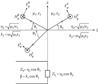
FIGURE 2.9
Oblique incidence of a p wave on a dielectric–dielectric interface. Transmission line analogy.
2.13Incidence of s Wave: Perpendicular-Polarized
Figure 2.10 shows an s wave propagating obliquely in x–z-plane. The transmission line analogy is also shown. Equations 2.90 and 2.91 still hold for the reasons mentioned before. The boundary conditions in this case can be stated as, at z = 0, for all t and x:
From the transmission line analogy shown in Figure 2.10 and Equation 2.66, the reflection and transmission coefficients are given respectively, by,
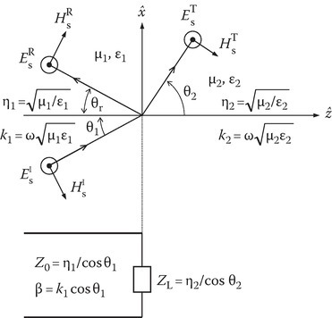
FIGURE 2.10
Oblique incidence of an s wave on a dielectric–dielectric interface. Transmission line analogy.
2.14Critical Angle and Surface Wave
Let us next consider wave propagation from an optically dense medium to an “optically rare” medium. In optics, a nonmagnetic medium is described in terms of the refractive index n, which is related to the dielectric constant through
The problem under consideration assumes that ε1 > ε2 or n1 > n2. From Snell’s law (Equation 2.91),
Note that θ2 > θ1 if n1 > n2. The angle of transmission θ2 = 90° when
Such an angle of incidence θc is called a critical angle. For this angle, the wave no longer propagates into medium 2 and in fact it propagates along the interface. However, we still have a reflected wave, with the angle of reflection θr = θc. The wave is said to be totally reflected since there is no power flow into medium 2. Since θ2 = 90°, the second medium for p wave propagation behaves like a short-circuited load and for s wave propagation as an open-circuited load. The magnitude of the reflection coefficient in either case is 1. The wave is totally reflected. Let us examine further what happens at the critical angle by considering s wave propagation. The reflection coefficient Γs = 1 and the transmission coefficient Ts = 2. Furthermore,
which represent a plane wave that travels along the interface in the positive x-direction. The time-averaged power densities of various waves are given by
Figure 2.11 shows the constant phase planes in medium 2.

FIGURE 2.11
Constant phase planes in medium 2 for θ1 = θc.
When the angle of incidence θ1 > θc, then
The equation can be satisfied only if θ2 is complex [2]:
The transmitted electric field may be written as
where
and the phase velocity of this wave is given by
This wave is a surface wave. The wave propagates in the positive x-direction but attenuates in the positive z-direction. Figure 2.12 shows the constant-amplitude planes (dotted lines) and the constant-phase planes (solid lines). The wave, while traveling along the interface with phase velocity vPe less than the phase velocity of an ordinary wave in the second medium vP2, rapidly decays in the z-direction. Such a wave is labeled as a tightly bound slow surface wave. The imaginary part of the complex Poynting vector 〈SI〉 = (1/2) Im[E × H*] represents the time-averaged reactive power density. For θ1 > θc, it may be shown that [3]
The wave penetrates the medium to a depth of 1/αe and the energy in the second medium is a stored energy. The wave in the second medium is called an evanescent wave. The attenuation of the evanescent wave is different from the attenuation of a traveling wave in a conducting medium. The former indicates the localization of wave energy near the interface. Because of this penetration, it may be shown that an optical beam of finite cross section will be displaced laterally relative to the incident beam at the boundary surface. This shift is known as the Goos–Hanschen shift and is discussed in [3].
FIGURE 2.12
Constant-phase planes and constant-amplitude planes, for θ1 > θc.
We will come across the evanescent wave in several other situations. The wave in a waveguide whose frequency is less than that of the cutoff frequency of the wave is an evanescent wave. The wave in a plasma medium, whose frequency is below “plasma frequency,” is an evanescent wave. The wave in the cladding of an optical fiber is an evanescent wave. Section 9.5 discusses the tunneling of power through a plasma slab by evanescent waves.
2.15One-Dimensional Cylindrical Wave and Bessel Functions
Let an infinitely long wire in free space be along the z-axis carrying a time harmonic current . From Equation 1.50, it is clear that the vector potential A will have only the z-component and from the symmetry it is also clear that the component is at the most a function of the cylindrical radial coordinate ρ:
From Equation 1.47 we get
Since A is a function of ρ only, Equation 2.117 becomes an ordinary differential equation of the form
which is the Bessel equation. It has two independent solutions J0 and Y0. These are analogous to cosine and sine functions that are the independent solutions for the Cartesian case. Linear combinations of J0 and Y0 give other functions to represent traveling waves in cylindrical coordinates. Table 2.2 gives the power series [4] for these functions and also differential and integral relations involving these functions. Table 2.3 lists these functions and also gives analogous functions in Cartesian coordinates. Since we are on the topic of Bessel functions, Jm and Ym are the solutions of a more general Bessel equation
The sketches of the functions Jm and Ym for various values of m and real values of the argument are given in Figure 2.13.
TABLE 2.2
Bessel Functions: Definitions and Relations
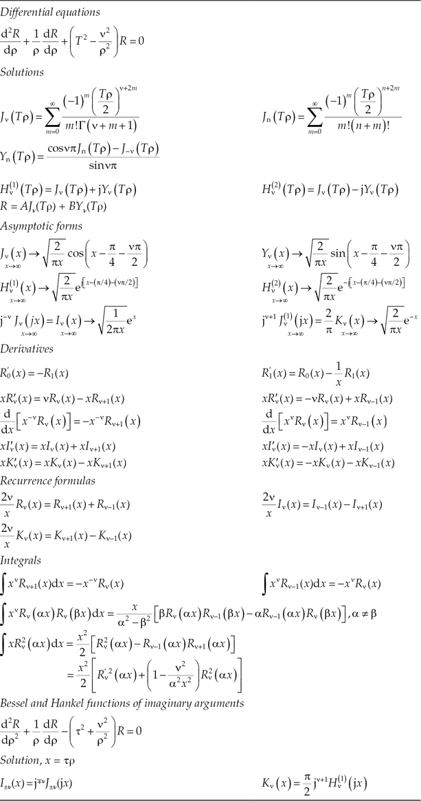
TABLE 2.3
Wave Functions in Cylindrical and Cartesian Coordinates

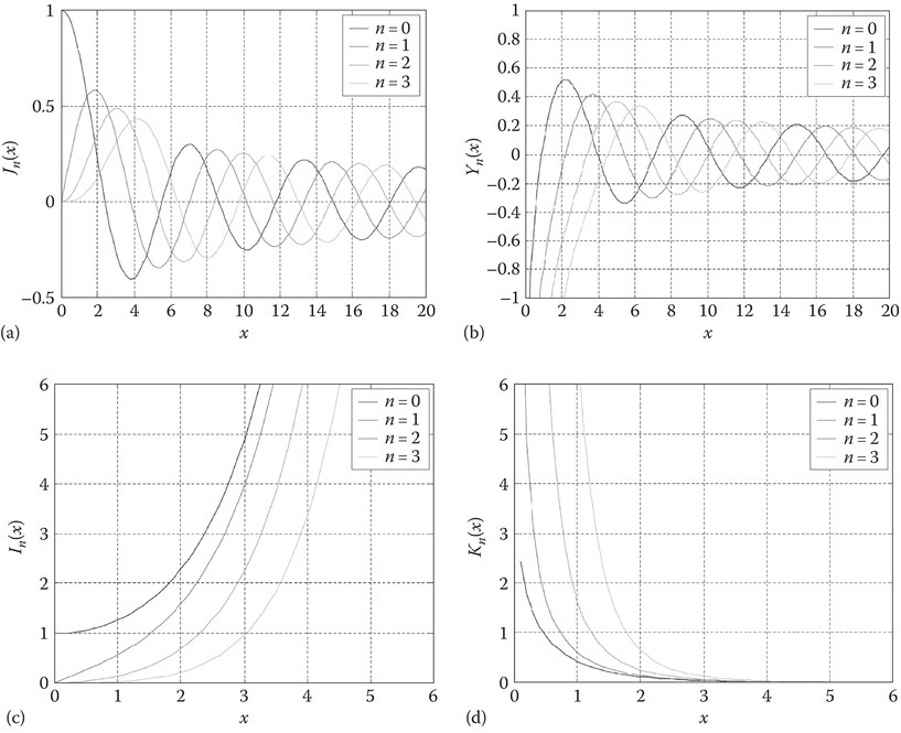
FIGURE 2.13
(a) Bessel functions of the first kind. (b) Bessel functions of the second kind. (c) Modified Bessel functions of the first kind. (d) Modified Bessel functions of the second kind.
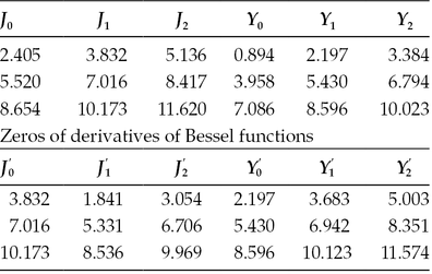
Table 2.4 lists the zeros χ mn of the Bessel function Jm and the zeros of the derivative of the Bessel function with respect to its argument. The second subscript n denotes the nth zero of these oscillatory functions. These higher-order Bessel functions will be used in solving the cylindrical waveguide problems.
TABLE 2.4
Zeros of Bessel Functions
Getting back to the subject of the electromagnetic fields due to harmonic current in an infinitely long wire, the solution of Equation 2.119 that fits the requirement of an outgoing wave as k0ρ tends to infinity is expressed in terms of a Hankel function of the second kind (see Table 2.2):
where A0 is a constant to be determined. All the components of the electric and magnetic fields may be obtained from Maxwell’s equations and Equation 2.121:
Application of Ampere’s law for a circular contour C in the x–y-plane of radius ρ, in the limit ρ → 0, relates the constant A0 to the current :
In obtaining Equation 2.126, the following small-argument approximation is used:
The fields and are given by
Equations 2.128 and 2.129 are the fields of a one-dimensional cylindrical wave. It can be shown that the wave impedance in the far-zone is
Since the wave impedance is equal to the intrinsic impedance of the medium, the wave is a TEM as shown in Figure 2.14.

FIGURE 2.14
One-dimensional cylindrical wave.
References
- 1.Ulaby, F.T., Applied Electromagnetics, Prentice Hall, Englewood Cliffs, NJ, 1999.
- 2.Balanis, C.A., Advanced Engineering Electromagnetics, Wiley, New York, 1989.
- 3.Lekner, J., Theory of Reflection, Kluwer Academic Publishers, Boston, MA, 1987.
- 4.Ramo, S., Whinnery, J.R., and Van Duzer, T.V., Fields and Waves in Communication Electronics, 3rd edition, Wiley, New York, 1994.