
]>
Appendix 8B: Left-Handed Materials and Transmission Line Analogies
8B.1Introduction
The material [1] discussed in this section is different from the left-handed chiral material discussed in Section 8.10. The qualifier “left-handed” is explained below.
Section 2.1 discussed the propagation of the uniform plane wave in a sourceless isotropic medium. It is shown that the unit vectors in the directions of the electric field E, magnetic field H, and the direction of propagation k are mutually orthogonal in the right-handed sense:
Such a material is considered a right-handed material, in contrast to an artificial material called the “left-handed material” [1,2,3,4,5,6,7,8]. In this artificial material,
Such a property arises in this artificial medium with negative permittivity ε and negative permeability μ. In that sense, some authors prefer to call it “double-negative” (DNG) medium. Some authors call it by yet another name “Veselago” medium, in honor of the scientist who discussed the properties of such a medium in a seminal paper [2] in 1968. Caloz and Itoh [8] explain metamaterials through the engineering approach, using the analogy with the transmission lines. The write-up in this section closely follows the approach of Caloz and Itoh [8].
Consider a transmission line, whose circuit representation of a differential length of a transmission line is given in Figure 8B.1.

FIGURE 8B.1
Circuit representation of an artificial transmission line.
The reason for using the subscripts R and L will become clear later on.
Following the approach of Section 2.7, we obtain the partial differential equation (PDE) for the voltage and the current:
The fourth-order PDE for the voltage variable is obtained by eliminating I, from Equations 8B.1 and 8B.2. The operator technique of replacing ∂/∂z by p and ∂/∂t by s will be useful in solving Equations 8B.1 and 8B.2 simultaneously. Note that ∫fdt will be replaced by f/s, where f stands for I or V. Thus, from Equation 8B.2, we get
In the operator form, Equation 8B.1 becomes
Substituting Equation 8B.3 into Equation 8B.4 to eliminate I and simplifying, we get
Reverting back to the derivative form, Equation 8B.5 will yield the PDE for the voltage:
For harmonic variation in space and time,
We obtain the following dispersion relation:
The ω−k diagram is obtained by tracing the curve given by Equation 8B.8 in the ω−k plane. The intersections with the ω-axis are obtained by substituting k = 0 in Equation 8B.8.
Let
noting that
we can write Equation 8B.9 in the form
Thus, the intersection points on the ω-axis are ω = ±ωsh and ω = ±ωse. The complete sketch of the ω−k diagram is given in Figure 8B.2, assuming that ωse < ωsh.

FIGURE 8B.2
ω−k diagram of the artificial transmission line given in Figure 9.6.
The subscripts LH and RH and the superscripts + and – in Figure 8B.2 are explained next.
The superscript + denotes a positive group velocity (positive slope of the ω−k curve) which in turn means energy flow in the positive z-direction. The superscript – denotes a negative group velocity which in turn means energy flow in the negative z-direction. The subscript RH denotes that the phase velocity and the group velocity have the same sign, the usual property of isotropic regular materials called right-handed materials. The subscript LH indicates opposite sign for the phase velocity and the group velocity, the property of the unusual materials called left-handed materials. In the LH case, the direction of power flow and the phase propagation are opposite to each other.
If ωse > ωsh, then the ω−k diagram is still given by Figure 8B.2, with ωse and ωsh interchanged. If ωse = ωsh, called balanced model, then the ω−k diagram degenerates into a simpler diagram shown in Figure 8B.3.

FIGURE 8B.3
ω−k diagram for a balanced transmission line model of Figure 9.6. ω0 = ωse = ωsh. The dotted curves are for PLH system and for PRH system.
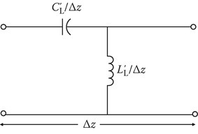
FIGURE 8B.4
Transmission line analogy to a PLH material.
The pure right-handed (PRH) system is obtained by making
Example 8B.1
In the equivalent circuit of a transmission line, for a length Δz, shown in Figure 8B.1, assume that
Sketch the ω−k diagram.
If ω = 0.8, then determine (i) phase velocity Vp, (ii) group velocity Vg, and (iii) wavelength λ.
Repeat (b), if ω = 1.
Repeat (b), if ω = 1.1.
Solution
From Equation 8B.8, the dispersion relation is given by
(8B.12)ω2k2+2ω2−1−ω4=0 and from Equations 8B.10a and 8B.10b,
(8B.13)ωse=1. (8B.14)ωsh=1. This is a balanced transmission line.
From Equation 8B.12,
(8B.15)ω2k2k2kVp====ω4−2ω2+1=(ω2−1)2,(ω2−1ω)2=(ω−1ω)2,±(ω−1ω),ωk=±ωω−1/ω=±ω2ω2−1, (8B.16)dkdωVg==±ddω(ω−1ω)=±ω2+1ω2,dωdk=±ω2ω2+1. The bottom sign in the expressions for Vp and Vg correspond to negative values of ω. The sketch of the ω−k diagram is shown by the solid line in Figure 8B.3, where ω0 = 1.
From Equations 8B.15 and 8B.16, we have
ω=0.8,Vp=ω2ω2−1∣∣ω=0.8=−1.78, Vg=ω2ω2+1∣∣ω=0.8=0.39, λ=2π|k|=2πω−1/ω∣∣ω=0.8=1.78.
ω = 1.0:
Vp=∞,Vg=12,λ=∞. ω = 1.1:
Vp=5.76,Vg=0.548,λ=32.91.
From this example, we see that the balanced transmission line behaves like a PLH material for ω < ω0 and as a PRH material for ω > ω0. In the neighborhood of ω ≈ ω0, the balanced transmission line differs considerably from PLH as well as PRH.
8B.2Electromagnetic Properties of a Left-Handed Material
Let us reverse the transmission line analogy to obtain the equivalent electromagnetic parameters εr and μr of a medium which has the same form as Equations 8B.1 and 8B.2. We will consider a TEM harmonic wave with
whereas Equations 8B.1 and 8B.2 yield for the phasors
Comparing Equation 8B.17 with Equation 8B.19, with
Note that the medium is dispersive since μ as well as ε are highly dispersive.
The relative permittivity εr and the relative permeability μr are given by
where ωse and ωsh are given by Equations 8B.10a and 8B.10b, respectively.
Figure 8B.5a sketches the variation of εr and μr with frequency ω and Figure 8B.5b sketches the refractive index n defined by

FIGURE 8B.5
Variation with frequency of (a) εr and μr and (b) refractive index n for the case ωsh < ωse. (Reproduced from Caloz, C. and Itoh, T. Electromagnetic Metamaterials, p. 68. Copyright Wiley. With permission.)
We note the following interesting features revealed by Figure 8B.5.
The variation of εr is similar to the variation of εp given by Equation 8B.8 for simple metals of Section 8.1, when collisions are neglected. The role of ωp is played by ωsh. εr is negative for ω < ωsh. Perhaps metals excited by electromagnetic wave of ω < ωsh can be the material with negative εr. Metals have high electron density and hence the plasma frequency is in the ultraviolet frequency range. At microwave frequency, εr is highly negative and the metal behaves as a good conductor dominated by collisions and we usually treat it as a good conductor of conductivity given by Equation 8.27, rather than a plasma in the cutoff region (see Figure 8.7). Pendry et al. [4,5] used an interesting calculation method to compute the plasma frequency of a metallic system consisting of thin wires.
So far, we have not discussed any material which has the variation of μr given in Figure 8B.5. Pendry et al. [6] suggested the possibility of constructing such a material in 1999, using a split ring structure in a square array.
From Figure 8B.5 of this section, we note when ω < ωsh and ω < ωse, εr as well as μr are negative and the refractive index n is also negative. In this case, the material is left-handed. Smith et al. [3] constructed such artificial materials and showed experimentally that such a material exhibited the properties of a left-handed material. The experiments were conducted in the microwave range.
In the frequency range ωsh < ω < ωse, εr is positive but μr is negative and the refractive index is imaginary and the wave is evanescent. This frequency domain is a stop band due to a negative μr and hence the band gap is called the magnetic gap. In the case ωse < ω < ωsh, the gap is called the electric gap.
A negative value for εr (μr) does not imply that the stored electric energy (magnetic energy) is negative. As we have noted, the material is dispersive and the stored energy for a dispersive medium is not given by (1/4)ε0εrE2((1/4)μ0μrH2) but by [1,9]
Substituting Equations 8B.23 and 8B.24 into Equations 8B.26 and 8B.27, respectively, we obtain
The refractive index
Equation 8B.25 can be written in an alternate form as
where
Equation 8B.31 is graphed in Figure 8B.5. The broken line is for the evanescent wave. nLH is negative and hence the alternative name for the LH material is NPV material.
8B.3Boundary Conditions, Reflection, and Transmission
The boundary conditions (Equation 1.14, Equation 1.15, Equation 1.16 and Equation 1.17) are valid even if one or both of the media are LHM, since these are derived from Maxwell’s equation. If ρs and K are zero, these are
where the subscripts n stands for the normal component and t stands for the tangential component. For the specific case of the medium 2 LHM and the medium 1 RHM, since μ2 and ε2 are negative, we have
A more general case can be considered by considering the sign of the electromagnetic parameters separately and writing
where s1 and s2 are +1 or −1 depending on whether the medium is RH or LH, respectively. Figure 8B.6 compares the transmission through the interface of the two media.
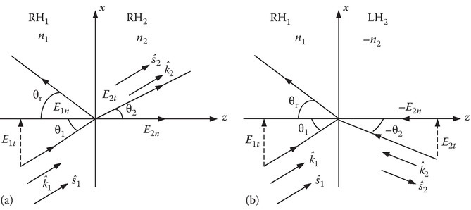
FIGURE 8B.6
Transmission through the interface: (a) both media are RH and (b) media 2 is LH with refractive index –n2.
The first part of Snell’s law
is the same for Figure 8B.6a and b, but the second part of the Snell’s law for RH–LH interface is given by
Thus, θt for the case of RH–LH interface is (−θ2) as shown in Figure 8B.6b. We can thus state Snell’s law in the general form as
Figure 8B.7 suggests that a “flat lens” consisting of RH, LH, and RH can focus and refocus if the three media have the same magnitude for n.

FIGURE 8B.7
Two symmetrical rays from the source is focused and refocused if the refractive indices of the three media have the same magnitude of n. (Reproduced from Caloz, C. and Itoh, T. 2006. Electromagnetic Metamaterials, p. 47. Copyright Wiley. With permission.)
If |nL| ≠ |nR|, then a pure focal point is not formed and the focal point gets diffused [1]. Moreover, the intrinsic impedances also satisfy the requirement
There will be no reflection. This can happen only if
This is obviously difficult to achieve, except perhaps for over a very narrow band of frequencies, even approximately, for a flat lens.
Pendry [10] discussed the phenomenon that LH materials can overcome diffraction limit of the conventional optics. He showed theoretically that an LH slab can overcome the diffraction limit (the resolution is limited by the wavelength) by choosing
Caloz and Itoh [1] discuss the enhancement of the evanescent wave by the LH slab.
8B.4Artificial Left-Handed Materials
Pendry et al. [4] showed that a long, thin, metallic wire array with a period p much less than the wavelength can produce a material with negative ε and positive μ. This artificial plasmonic type of structure has
In the above, p is the cell size, ωpe the plasma frequency, given by Equation 8.22 for a real plasma, a the radius of the metallic thin wire of conductivity σ, and ν the collision frequency. The wire length l is taken as infinity (a ≪ l) (Figure 8B.8).
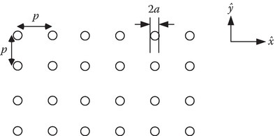
FIGURE 8B.8
Cross section of a thin-wire plasmonic structure.
Equations 8B.47 and 8B.48 are derived, assuming the electric field is in the z-direction, the wires are thin and long (a ≪ l), p ≪ λ, and the radius a ≪ p ≪ l. The restriction p ≪ λ is equivalent to saying that the differential model used in Figure 8B.1 (Δz ~ p) can be used. The experimental results for the structure with the following data are
The wire material, aluminum (N = 1.806 × 1029/m3), showed a plasma frequency fpe = 8.3 GHz. Had we used (Equation 8.22) with N given above, we would have got a plasma frequency in an ultraviolet frequency band. Pendry showed that the reduction of the plasma frequency of the structure is due to the constraint that electrons are forced to move along the thin wires. Since only a part of the space is filled with metal, the effective electron density Neff is given by
The electrons in the magnetic field created by the current in the wire experience additional momentum. The effect of this additional momentum can be accounted for by considering an effective value meff for the mass of the electron given by
The plasma frequency, using the effective values for the electron density and the mass of the electron, is given by
Substituting Equations 8B.51 and 8B.52 into Equation 8B.53, we get Equation 8B.47. For the data of Equations 8B.49 and 8B.50, the plasma frequency turns out to be
close to the experimental value.
Equations 8B.47 and 8B.48 can also be obtained by considering the array as a “periodically spaced wire gratings or periodically spaced loaded transmission line” [1].
The permeability of the wire structure made of nonmagnetic conducting material such as copper or aluminum will be μ0. The assumption that l ≫ λ means that the wires are excited at frequencies much less than the first resonance.
Pendry et al. [6] discussed a negative −μ artificial element, which is a metal split–ring resonator (SRR) shown in Figure 8B.9; Figure 8B.9a shows one SRR element and Figure 8B.9b shows the array structure.
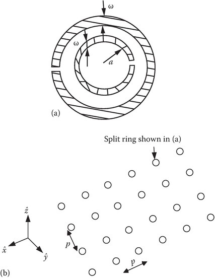
FIGURE 8B.9
Negative −μ resonant structure: (a) SRR element and (b) SRR structure.
The structure is excited by a magnetic field perpendicular to the plane of the ring. Such a structure exhibits a plasmonic-type permeability frequency function given by (ignoring losses) [1,6]
where
In the above equations, p is the spatial period, a the inner radius of the smaller ring, w the width of the rings, and δ the radial spacing between the rings, as marked in Figure 8B.9a. From Equation 8B.55, we note that μr > 1, for 1 < w < wom, has resonance (μr = ∞) at w = wom, negative in the frequency domain wom < w < wpm, where
First experimental LH material based on the combination of the thin-wire structure with the SRR was constructed by Smith et al. [3]. Caloz and Itoh [1, p. 8, Figure 1.4a] show a three-dimensional sketch of such a structure and remark that it is mono-dimensionally LH, since only “one direction” is allowed for the doublet (E, H): εxx < 0, 0 < ω < ωpe; μxx < 0, ωom < ω < ωpm (Figure 8B.10).

FIGURE 8B.10
Sketch of μr vs. w for split–ring resonate structure.
A planar LH structure in microstrip technology consisting of series interdigital capacitors and shunt stub inductors was investigated [11,12] and summarized in [1].
References
- 1.Caloz, C. and Itoh, T., Electromagnetic Metamaterials, Wiley, Hoboken, NJ, 2006.
- 2.Veselago, V., The electrodynamics of substances with simultaneously negative values of ε and μ, Soviet Phys.Uspekhi, 10(4), 509–514, 1968.
- 3.Smith, D.R., Padilla, W.J., Vier, D. C., Nemat-Nasser, S. C., and Schultz, S., Composite medium with simultaneously negative permeability and permittivity, Phys. Rev. Lett., 84(18), 4184–4187, 2000.
- 4.Pendry, J.B., Holden, A. J., Stewart, W. J., and Youngs, I., Extremely low frequency plasmons in metallic mesostructure, Phys. Rev. Lett., 76(25), 4773–4776, 1996.
- 5.Pendry, J.B., Holden, A. J., Robbins, D. J., and Stewart, W. J., Low frequency plasmons in thin-wire structure, J. Phys. Condens. Matter, 10, 4785–4809, 1998.
- 6.Pendry, J.B., Holden, A. J., Robbins, D. J., and Stewart, W. J., Magnetism from conductors and enhanced nonlinear phenomena, IEEE Trans. Microw. Theory. Tech., 47(11), 2075–2084, 1999.
- 7.Smith, D. R., Vier, D. C., Kroll, N., and Schultz, S., Direct calculation of permeability and permittivity for a left-handed metamaterial, App. Phys. Lett., 77(14), 2246–2248, 2000.
- 8.Sheley, R. A., Smith, D. R., and Schultz, S., Experimental verification of a negative index of refraction, Science, 292, 77–79, 2001.
- 9.Papas, C. H., Theory of Electromagnetic Wave Propagation, McGraw-Hill, New York, 1965.
- 10.Pendry, J. B., Negative refraction makes a perfect lens, Phys. Rev. Lett., 85(18), 3966–3969, 2000.
- 11.Caloz, C. and Itoh, T., Application of the transmission line theory of left-handed (LH) materials to the realization of a microstrip LH transmission line, in Proceedings of IEEE-AP-S USNC/URSI National Radio Science Meeting, Vol. 2, San Antonio, TX, June 2002, pp. 412–415.
- 12.Caloz, C. and Itoh, T., Transmission line approach of left-handed (LH) structures and microstrip realization of a low-loss broadband LH filter, IEEE Trans. Antennas Propag., 52(5), 1159–1166, 2004.