
4.3 Constructing Gates
Before we examine how gates are connected to form circuits, let’s examine, at an even more basic level, how a gate is constructed to control the flow of electricity.
Transistors
A gate uses one or more transistors to establish how the input values map to the output value. A transistor is a device that acts, depending on the voltage level of the input signal, either as a wire that conducts electricity or as a resistor that blocks the flow of electricity. A transistor has no moving parts, yet it acts like a switch. It is made of a semiconductor material, which is neither a particularly good conductor of electricity (such as copper) nor a particularly good insulator (such as rubber). Usually silicon is used to create transistors.
In Chapter 1, we mentioned that the invention of transistors, which occurred in 1947 at Bell Labs, changed the face of technology, ushering in the second generation of computer hardware. Before the advent of transistors, digital circuits used vacuum tubes, which dissipated a great deal of heat and often failed, requiring replacement. Transistors are much smaller than vacuum tubes and require less energy to operate. They can switch states in a few nanoseconds. Computing, as we know it today, is largely due to the invention of the transistor.
Before tackling the details of transistors, let’s discuss some basic principles of electricity. An electrical signal has a source, such as a battery or an outlet in your wall. If the electrical signal is grounded, it is allowed to flow through an alternative route to the ground (literally), where it can do no harm. A grounded electrical signal is pulled down, or reduced, to 0 volts.
A transistor has three terminals: a source, a base, and an emitter. The emitter is typically connected to a ground wire, as shown in FIGURE 4.8. For computers, the source produces a high voltage value, approximately 5 volts. The base value regulates a gate that determines whether the connection between the source and ground is made. If the source signal is grounded, it is pulled down to 0 volts. If the base does not ground the source signal, it stays high.
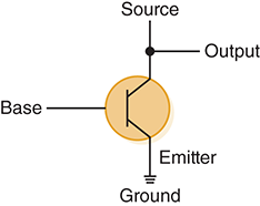
FIGURE 4.8 The connections of a transistor
An output line is usually connected to the source line. If the source signal is pulled to the ground by the transistor, the output signal is low, representing a binary 0. If the source signal remains high, so does the output signal, representing a binary 1.
The transistor is either on, producing a high-output signal, or off, producing a low-output signal. This output is determined by the base electrical signal. If the base signal is high (close to a +5 voltage), the source signal is grounded, which turns the transistor off. If the base signal is low (close to a 0 voltage), the source signal stays high, and the transistor is on.
Now let’s see how a transistor is used to create various types of gates. It turns out that, because of the way a transistor works, the easiest gates to create are the NOT, NAND, and NOR gates. FIGURE 4.9 shows how these gates can be constructed using transistors.

FIGURE 4.9 Constructing gates using transistors
The diagram for the NOT gate is essentially the same as our original transistor diagram. It takes only one transistor to create a NOT gate. The signal Vin represents the input signal to the NOT gate. If it is high, the source is grounded and the output signal Vout is low. If Vin is low, the source is not grounded and Vout is high. Thus the input signal is inverted, which is exactly what a NOT gate does.
The NAND gate requires two transistors. The input signals V1 and V2 represent the input to the NAND gate. If both input signals are high, the source is grounded and the output Vout is low. If either input signal is low, however, one transistor or the other keeps the source signal from being grounded and the output is high. Therefore, if V1 or V2 or both carry a low signal (binary 0), the output is a 1. This is consistent with the processing of a NAND gate.
The construction of a NOR gate also requires two transistors. Once again, V1 and V2 represent the input to the gate. This time, however, the transistors are not connected in series. The source connects to each transistor separately. If either transistor allows the source signal to be grounded, the output is 0. Therefore, the output is high (binary 1) only when both V1 and V2 are low (binary 0), which is what we want for a NOR gate.
An AND gate produces output that is exactly opposite of the NAND output of a gate. Therefore, to construct an AND gate, we simply pass the output of a NAND gate through an inverter (a NOT gate). That’s why AND gates are more complicated to construct than NAND gates: They require three transistors, two for the NAND and one for the NOT. The same reasoning can be applied to understand the relationship between NOR and OR gates.