
DC-DC Converters
Dariusz Czarkowski New York University, New York, NY, United States
Abstract
Modern electronic systems require high-quality, small, lightweight, reliable, and efficient power supplies. Linear power regulators, whose principle of operation is based on a voltage or current divider, are inefficient. They are limited to output voltages smaller than the input voltage. Also, their power density is low because they require low-frequency (50 or 60 Hz) line transformers and filters. Linear regulators can, however, provide a very high-quality output voltage. Their main area of application is at low power levels as low-dropout voltage (LDO) regulators. Electronic devices in linear regulators operate in their active (linear) modes. At higher power levels, switching regulators are used. Switching regulators use power electronic semiconductor switches in on and off states. Since there is a small power loss in those states (low voltage across a switch in the on state, zero current through a switch in the off state), switching regulators can achieve high energy conversion efficiencies. Modern power electronic switches can operate at high frequencies. The higher the operating frequency, the smaller and lighter the transformers, filter inductors, and capacitors. In addition, dynamic characteristics of converters improve with increasing operating frequencies. The bandwidth of a control loop is usually determined by the corner frequency of the output filter. Therefore, high operating frequencies allow for achieving a faster dynamic response to rapid changes in the load current and/or the input voltage.
Keywords
DC Choppers; Continuous conduction mode; Discontinuous conduction mode; Converters; Forward converter; Push-pull converter
10.1 Introduction
Modern electronic systems require high-quality, small, lightweight, reliable, and efficient power supplies. Linear power regulators, whose principle of operation is based on a voltage or current divider, are inefficient. They are limited to output voltages smaller than the input voltage. Also, their power density is low because they require low-frequency (50 or 60 Hz) line transformers and filters. Linear regulators can, however, provide a very high-quality output voltage. Their main area of application is at low power levels as low-dropout voltage (LDO) regulators. Electronic devices in linear regulators operate in their active (linear) modes. At higher power levels, switching regulators are used. Switching regulators use power electronic semiconductor switches in on and off states. Since there is a small power loss in those states (low voltage across a switch in the on state, zero current through a switch in the off state), switching regulators can achieve high energy conversion efficiencies. Modern power electronic switches can operate at high frequencies. The higher the operating frequency, the smaller and lighter the transformers, filter inductors, and capacitors. In addition, dynamic characteristics of converters improve with increasing operating frequencies. The bandwidth of a control loop is usually determined by the corner frequency of the output filter. Therefore, high operating frequencies allow for achieving a faster dynamic response to rapid changes in the load current and/or the input voltage.
High-frequency electronic power processors are used in dc-dc power conversion. The functions of dc-dc converters are
• to convert a dc input voltage VS into a dc output voltage VO,
• to regulate the dc output voltage against load and line variations,
• to reduce the ac voltage ripple on the dc output voltage below the required level,
• to provide isolation between the input source and the load (isolation is not always required),
• to protect the supplied system and the input source from electromagnetic interference (EMI),
• to satisfy various international and national safety standards.
The dc-dc converters can be divided into two main types: hard-switching pulse-width-modulated (PWM) converters and resonant and soft-switching converters. This chapter deals with the former type of dc-dc converters. The PWM converters have been very popular for the last three decades. They are widely used at all power levels. Topologies and properties of PWM converters are well understood and described in literature. Advantages of PWM converters include low component count, high efficiency, constant frequency operation, relatively simple control and commercial availability of integrated circuit controllers, and ability to achieve high conversion ratios for both step-down and step-up application. A disadvantage of PWM dc-dc converters is that PWM rectangular voltage and current waveforms cause turn-on and turn-off losses in semiconductor devices that limit practical operating frequencies to a megahertz range. Rectangular waveforms also inherently generate EMI.
This chapter starts from a section on dc choppers that are used primarily in dc drives. The output voltage of dc choppers is controlled by adjusting the on time of a switch, which in turn adjusts the width of a voltage pulse at the output. This is the so-called pulse-width-modulation (PWM) control. The dc choppers with additional filtering components form PWM dc-dc converters. Four basic dc-dc converter topologies are presented in Sections 10.3–10.6: buck, boost, buck-boost, and Ćuk converters. Popular isolated versions of these converters are also discussed. Operation of converters is explained under ideal component and semiconductor device assumptions. Section 10.7 discusses effects of nonidealities in PWM converters. Section 10.8 presents topologies for increased efficiency at low output voltage and for bidirectional power flow. Section 10.9 reviews control principles of PWM dc-dc converters. Two main control schemes, voltage-mode control and current-mode control, are described. Summary of application areas of PWM dc-dc converters is given in Section 10.10. Finally, a list of modern textbooks on power electronics is provided. These books are excellent resources for deeper exploration of the area of dc-dc power conversion.
10.2 DC Choppers
A step-down dc chopper with a resistive load is shown in Fig. 10.1A. It is a series connection of a dc input voltage source VS, controllable switch S, and load resistance R. In most cases, switch S has a unidirectional voltage blocking capabilities and unidirectional current conduction capabilities. Power electronic switches are usually implemented with power MOSFETs, IGBTs, MCTs, power BJTs, or GTOs. If an antiparallel diode is used or embedded in a switch, a switch exhibits a bidirectional current conduction property. Fig. 10.1B depicts waveforms in a step-down chopper. The switch is being operated with a duty ratio D defined as a ratio of the switch on time to the sum of the on and the off times. For a constant frequency operation,
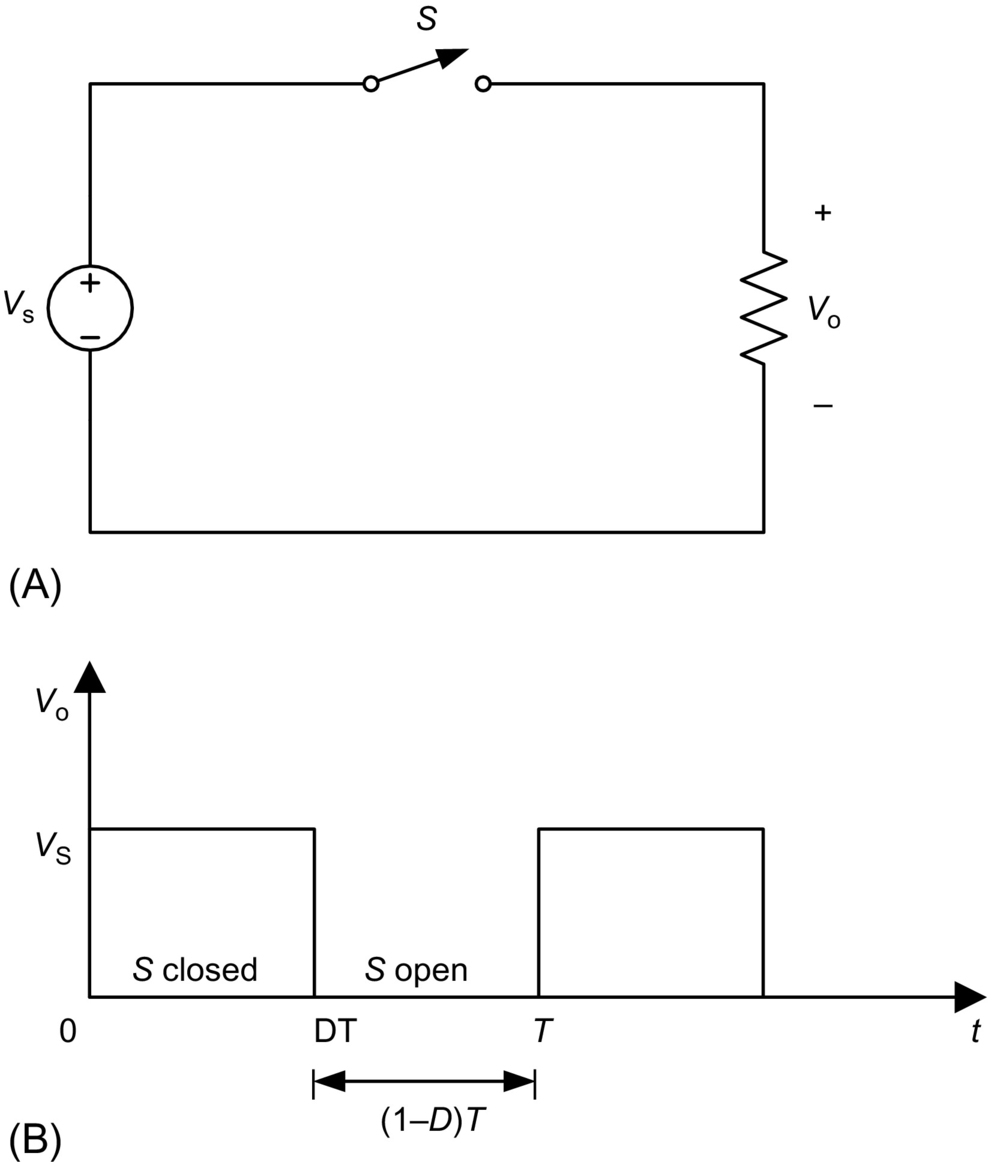
D≡tonton+toff=tonT
where T=1/f is the period of the switching frequency f. The average value of the output voltage is
VO=DVS
and can be regulated by adjusting duty ratio D. The average output voltage is always smaller than the input voltage, hence, the name of the converter.
The dc step-down choppers are commonly used in dc drives. In such a case, the load is presented as a series combination of inductance L, resistance R, and back emf E as shown in Fig. 10.2A. To provide a path for a continuous inductor current flow when the switch is in the off state, an antiparallel diode D must be connected across the load. Since the chopper of Fig. 10.2A provides a positive voltage and a positive current to the load, it is called a first-quadrant chopper. The load voltage and current are graphed in Fig. 10.2B under assumptions that the load current never reaches zero and the load time constant τ=L/R![]() is much greater than the period T. Average values of the output voltage and current can be adjusted by changing the duty ratio D.
is much greater than the period T. Average values of the output voltage and current can be adjusted by changing the duty ratio D.

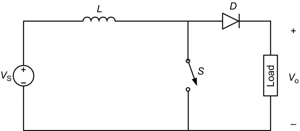
The dc choppers can also provide peak output voltages higher than the input voltage. Such a step-up configuration is presented in Fig. 10.3. It consists of dc input source VS, inductor L connected in series with the source, switch S connecting the inductor to ground, and a series combination of diode D and load. If the switch operates with a duty ratio D, the output voltage is a series of pulses of duration (1−D)T![]() and amplitude VS/(1−D)
and amplitude VS/(1−D)![]() . Neglecting losses, the average value of the output voltage is VS. To obtain an average value of the output voltage greater than VS, a capacitor must be connected in parallel with the load. This results in a topology of a boost dc-dc converter that is described in Section 10.4.
. Neglecting losses, the average value of the output voltage is VS. To obtain an average value of the output voltage greater than VS, a capacitor must be connected in parallel with the load. This results in a topology of a boost dc-dc converter that is described in Section 10.4.
10.3 Step-Down (Buck) Converter
10.3.1 Basic Converter
The step-down dc-dc converter, commonly known as a buck converter, is shown in Fig. 10.4A. It consists of dc input voltage source VS, controlled switch S, diode D, filter inductor L, filter capacitor C, and load resistance R. Typical waveforms in the converter are shown in Fig. 10.4B under assumption that the inductor current is always positive. The state of the converter in which the inductor current is never zero for any period of time is called the continuous conduction mode (CCM). It can be seen from the circuit that when the switch S is commanded to the on state, the diode D is reverse biased. When the switch S is off, the diode conducts to support an uninterrupted current in the inductor.

The relationship among the input voltage, output voltage, and the switch duty ratio D can be derived, for instance, from the inductor voltage vL waveform (see Fig. 10.4B). According to Faraday's law, the inductor volt-second product over a period of steady-state operation is zero. For the buck converter,
(VS−VO)DT=−VO(1−D)T
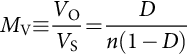
Hence, the dc voltage transfer function, defined as the ratio of the output voltage to the input voltage, is
MV≡VOVS=D
It can be seen from Eq. (10.4) that the output voltage is always smaller than the input voltage.
The dc-dc converters can operate in two distinct modes with respect to the inductor current iL. Fig. 10.4B depicts the CCM in which the inductor current is always greater than zero. When the average value of the input current is low (high R) and/or the switching frequency f is low, the converter may enter the discontinuous conduction mode (DCM). In the DCM, the inductor current is zero during a portion of the switching period. The CCM is preferred for high efficiency and good utilization of semiconductor switches and passive components. The DCM may be used in applications with special control requirements, since the dynamic order of the converter is reduced (the energy stored in the inductor is zero at the beginning and at the end of each switching period). It is uncommon to mix these two operating modes because of different control algorithms. For the buck converter, the value of the filter inductance that determines the boundary between CCM and DCM is given by
Lb=(1−D)R2f
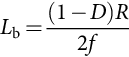
For typical values of D=0.5![]() , R=10Ω
, R=10Ω![]() , and f=100kHz
, and f=100kHz![]() , the boundary is Lb=25μH
, the boundary is Lb=25μH![]() . For L>Lb
. For L>Lb![]() , the converter operates in the CCM.
, the converter operates in the CCM.
The filter inductor current iL in the CCM consists of a dc component IO with a superimposed triangular ac component. Almost all of this ac component flows through the filter capacitor as a current ic. Current ic causes a small voltage ripple across the dc output voltage VO. To limit the peak-to-peak value of the ripple voltage below certain value Vr, the filter capacitance C must be greater than
Cmin=(1−D)VO8VrLf2
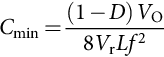
At D=0.5![]() , Vr/VO=1%
, Vr/VO=1%![]() , L=25μH
, L=25μH![]() , and f=100kHz
, and f=100kHz![]() , the minimum capacitance is Cmin=25μF
, the minimum capacitance is Cmin=25μF![]() .
.
Eqs. (10.5) and (10.6) are the key design equations for the buck converter. The input and output dc voltages (hence the duty ratio D) and the range of load resistance R are usually determined by preliminary specifications. The designer needs to determine values of passive components L and C and of the switching frequency f. The value of the filter inductor L is calculated from the CCM/DCM condition using Eq. (10.5). The value of the filter capacitor C is obtained from the voltage ripple condition Eq. (10.6). For the compactness and low conduction losses of a converter, it is desirable to use small passive components. Eqs. (10.5) and (10.6) show that it can be accomplished by using a high switching frequency f. The switching frequency is limited, however, by the type of semiconductor switches used and by switching losses. It should be also noted that values of L and C may be altered by effects of parasitic components in the converter, especially by the equivalent series resistance of the capacitor. The issue of parasitic components in dc-dc converters is discussed in Section 10.7.
10.3.2 Transformer Versions of Buck Converter
In many dc power supplies, a galvanic isolation between the dc or ac input and the dc output is required for safety and reliability. An economical mean of achieving such an isolation is to employ a transformer version of a dc-dc converter. High-frequency transformers are of a small size and weight and provide high efficiency. Their turns ratio can be used to additionally adjust the output voltage level. Among buck-derived dc-dc converters, the most popular are forward converter, push-pull converter, half-bridge converter, and full-bridge converter.
10.3.2.1 Forward Converter
The circuit diagram of a forward converter is depicted in Fig. 10.5. When the switch S is on, diode D1 conducts, and diode D2 is off. The energy is transferred from the input, through the transformer, to the output filter. When the switch is off, the state of diodes D1 and D2 is reversed. The dc voltage transfer function of the forward converter is

MV=Dn

where n=N1/N2![]() .
.
In the forward converter, the energy-transfer current flows through the transformer in one direction. Hence, an additional winding with diode D3 is needed to bring the magnetizing current of the transformer to zero. This prevents transformer saturation. The turns ratio N1/N3 should be selected in such a way that the magnetizing current decreases to zero during a fraction of the time interval when the switch is off.
Eqs. (10.5) and (10.6) can be used to design the filter components. The forward converter is very popular for low-power applications. For medium power levels, converters with bidirectional transformer excitation (push-pull, half bridge, and full bridge) are preferred due to better utilization of magnetic components.
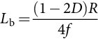
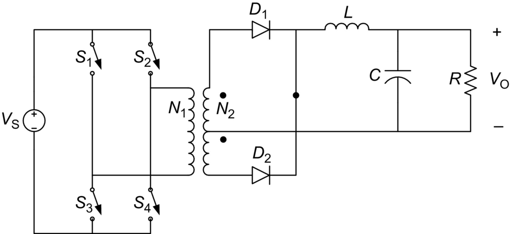
10.3.2.2 Push-Pull Converter
The PWM dc-dc push-pull converter is shown in Fig. 10.6. The switches S1 and S2 operate shifted in phase by T/2 with the same duty ratio D. The duty ratio must be smaller than 0.5. When switch S1 is on, diode D1 conducts, and diode D2 is off. Diode states are reversed when switch S2 is on. When both controllable switches are off, the diodes are on and share equally the filter inductor current. The dc voltage transfer function of the push-pull converter is

MV=2Dn

where n=N1/N2![]() . The boundary value of the filter inductor is
. The boundary value of the filter inductor is
Lb=(1−2D)R4f
The filter capacitor can be obtained from
Cmin=(1−2D)VO32VrLf2

10.3.2.3 Half-Bridge Converter
Fig. 10.7 shows the dc-dc half-bridge converter. The operation of the PWM half-bridge converter is similar to that of the push-pull converter. In comparison with the push-pull converter, the primary of the transformer is simplified at the expense of two voltage-sharing input capacitors. The half-bridge converter dc voltage transfer function is

MV≡VDVS=Dn

where D≤0.5.![]() Eqs. (10.9) and (10.10) apply to the filter components of this converter.
Eqs. (10.9) and (10.10) apply to the filter components of this converter.
10.3.2.4 Full-Bridge Converter
Comparing the PWM dc-dc full-bridge converter of Fig. 10.8 with the half-bridge converter, it can be seen that the input capacitors have been replaced by two controllable switches. The controllable switches are operated in pairs. When S1 and S4 are on, voltage VS is applied to the primary of the transformer, and diode D1 conducts. With S2 and S3 on, there is voltage −VS![]() across the primary transformer, and diode D2 is on. With all controllable switches off, both diodes conduct, similarly as in the push-pull and half-bridge converters. The dc voltage transfer function of the full-bridge converter is
across the primary transformer, and diode D2 is on. With all controllable switches off, both diodes conduct, similarly as in the push-pull and half-bridge converters. The dc voltage transfer function of the full-bridge converter is
MV≡VOVS=2Dn
where D≤0.5![]() . Values of filter components can be obtained from Eqs. (10.9) and (10.10).
. Values of filter components can be obtained from Eqs. (10.9) and (10.10).
It should be stressed that the full-bridge topology is a very versatile one. With different control algorithms, it is very popular in dc-ac conversion (square-wave and PWM single-phase inverters). It is also used in four-quadrant dc drives.
10.4 Step-Up (Boost) Converter
Fig. 10.9A depicts a step-up or a PWM boost converter. It is composed of dc input voltage source VS, boost inductor L, controlled switch S, diode D, filter capacitor C, and load resistance R. The converter waveforms in the CCM are presented in Fig. 10.9B. When the switch S is in the on state, the current in the boost inductor increases linearly. The diode D is off at the time. When the switch S is turned off, the energy stored in the inductor is released through the diode to the input RC circuit.

Using the Faraday's law for the boost inductor,
VSDT=(VO−VS)(1−D)T
from which the dc voltage transfer function turns out to be
MV≡VOVS=11−D

As the name of the converter suggests, the output voltage is always greater than the input voltage.
The boost converter operates in the CCM for L>Lb![]() where
where
Lb=(1−D)2DR2f

For D=0.5![]() , R=10Ω
, R=10Ω![]() , and f=100kHz
, and f=100kHz![]() , the boundary value of the inductance is Lb=6.25μH
, the boundary value of the inductance is Lb=6.25μH![]() .
.
As shown in Fig. 10.9B, the current supplied to the output RC circuit is discontinuous. Thus, a larger filter capacitor is required in comparison with that in the buck-derived converters to limit the output voltage ripple. The filter capacitor must provide the output dc current to the load when the diode D is off. The minimum value of the filter capacitance that results in the voltage ripple Vr is given by
Cmin=DVOVrRf
At D=0.5![]() , Vr/VO=1%
, Vr/VO=1%![]() , R=10Ω
, R=10Ω![]() , and f=100kHz
, and f=100kHz![]() , the minimum capacitance for the boost converter is Cmin=50μF
, the minimum capacitance for the boost converter is Cmin=50μF![]() .
.
The boost converter does not have a popular transformer (isolated) version.
10.5 Buck-Boost Converter
10.5.1 Basic Converter
A nonisolated (transformerless) topology of the buck-boost converter is shown in Fig. 10.10A. The converter consists of dc input voltage source VS, controlled switch S, inductor L, diode D, filter capacitor C, and load resistance R. With the switch on, the inductor current increases, while the diode is maintained off. When the switch is turned off, the diode provides a path for the inductor current. Note the polarity of the diode that results in its current being drawn from the output.

The buck-boost converter waveforms are depicted in Fig. 10.10B. The condition of a zero volt-second product for the inductor in steady state yields
VSDT=−VO(1−D)T
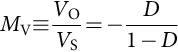
Hence, the dc voltage transfer function of the buck-boost converter is
MV≡VOVS=−D1−D

The output voltage VO is negative with respect to the ground. Its magnitude can be either greater or smaller (equal at D=0.5![]() ) than the input voltage as the converter's name implies.
) than the input voltage as the converter's name implies.
The value of the inductor that determines the boundary between the CCM and DCM is
Lb=(1−D)2R2f
The structure of the output part of the converter is similar to that of the boost converter (reversed polarities being the only difference). Thus, the value of the filter capacitor can be obtained from Eq. (10.16).
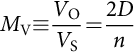
10.5.2 Flyback Converter
A PWM flyback converter is a very practical isolated version of the buck-boost converter. The circuit of the flyback converter is presented in Fig. 10.11A. The inductor of the buck-boost converter has been replaced by a flyback transformer. The input dc source VS and switch S are connected in series with the primary transformer. The diode D and the RC output circuit are connected in series with the secondary of the flyback transformer. Fig. 10.11B shows the converter with a simple flyback transformer model. The model includes a magnetizing inductance Lm and an ideal transformer with a turns ratio n=N1/N2![]() . The flyback transformer leakage inductances and losses are neglected in the model. It should be noted that leakage inductances, although not important from the principle of operation point of view, affect adversely switch and diode transitions. Snubbers are usually required in flyback converters.
. The flyback transformer leakage inductances and losses are neglected in the model. It should be noted that leakage inductances, although not important from the principle of operation point of view, affect adversely switch and diode transitions. Snubbers are usually required in flyback converters.
Refer to Fig. 10.11B for the converter operation. When the switch S is on, the current in the magnetizing inductance increases linearly. The diode D is off, and there is no current in the ideal transformer windings. When the switch is turned off, the magnetizing inductance current is diverted into the ideal transformer, the diode turns on, and the transformed magnetizing inductance current is supplied to the RC load. The dc voltage transfer function of the flyback converter is
MV≡VOVS=Dn(1−D)
It differs from the buck-boost converter voltage transfer function by the turns ratio factor n. A positive sign has been obtained by an appropriate coupling of the transformer windings.
Unlike in transformer buck-derived converters, the magnetizing inductance Lm of the flyback transformer is an important design parameter. The value of the magnetizing inductance that determines the boundary between the CCM and DCM is given by
Lmb=n2(1−D)2R2f
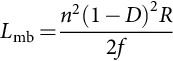
The value of the filter capacitance can be calculated using Eq. (10.16).
10.6 Ćuk Converter
The circuit of the Ćuk converter is shown in Fig. 10.12A. It consists of dc input voltage source VS, input inductor L1, controllable switch S, energy-transfer capacitor C1, diode D, filter inductor L2, filter capacitor C, and load resistance R. An important advantage of this topology is a continuous current at both the input and the output of the converter. Disadvantages of the Ćuk converter include a high number of reactive components and high current stresses on the switch, the diode, and the capacitor C1. Main waveforms in the converter are presented in Fig. 10.12B. When the switch is on, the diode is off, and the capacitor C1 is discharged by the inductor L2 current. With the switch in the off state, the diode conducts currents of the inductors L1 and L2, whereas capacitor C1 is charged by the inductor L1 current.

To obtain the dc voltage transfer function of the converter, we shall use the principle that the average current through a capacitor is zero for steady-state operation. Let us assume that inductors L1 and L2 are large enough that their ripple current can be neglected. Capacitor C1 is in a steady state if
IL2DT=IL1(1−D)T
For a lossless converter,
PS=VSIL1=−VOIL2=PO
Combining these two equations, the dc voltage transfer function of the Ćuk converter is
MV≡VOVS=−D1−D
This voltage transfer function is the same as that for the buck-boost converter.
The boundaries between the CCM and DCM are determined by
Lb1=(1−D)R2Df

for L1 and
Lb2=(1−D)R2f

for L2.
The output part of the Ćuk converter is similar to that of the buck converter. Hence, the expression for the filter capacitor C is
Cmin=(1−D)VO8VrL2f2

The peak-to-peak ripple voltage in the capacitor C1 can be estimated as
Vr1=DVOC1Rf

A transformer (isolated) version of the Ćuk converter can be obtained by splitting capacitor C1 and inserting a high-frequency transformer between the split capacitors.
10.7 Effects of Parasitic Components
The analysis of converters in Sections 10.2–10.6 has been performed under ideal switch, diode, and passive component assumptions. Nonidealities or parasitics of practical devices and components may, however, greatly affect some performance parameters of dc-dc converters. In this section, effects of parasitics on output voltage ripple, efficiency, and voltage transfer function of converters will be illustrated.
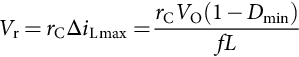
A more realistic model of a capacitor than just a capacitance C consists of a series connection of capacitance C and resistance rC. The resistance rC is called an equivalent series resistance (ESR) of the capacitor and is due to losses in the dielectric and physical resistance of leads and connections. Recall Eq. (10.6) that provided a value of the filter capacitance in a buck converter that limits the peak-to-peak output voltage ripple to Vr. The equation was derived under an assumption that the entire triangular ac component of the inductor current flows through a capacitance C. It is, however, closer to reality to maintain that this triangular component flows through a series connection of capacitance C and resistance rC.
The peak-to-peak ripple voltage is independent of the voltage across the filter capacitor and is determined only by the ripple voltage of the ESR if the following condition is satisfied:
C≥Cmin=max{1−Dmin2rCf,Dmax2rCf}
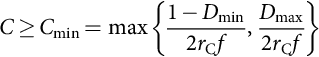
If condition (10.29) is satisfied, the peak-to-peak ripple voltage of the buck and forward converters is
Vr=rCΔiLmax=rCVO(1−Dmin)fL
For push-pull, half-bridge, and full-bridge converters,
C≥Cmin=max{0.5−Dmin2rCf,Dmax2rCf}
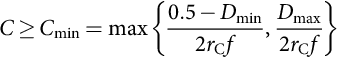
where Dmax≤0.5![]() . If condition (10.31) is met, the peak-to-peak ripple voltage Vr of these converters is given by
. If condition (10.31) is met, the peak-to-peak ripple voltage Vr of these converters is given by
Vr=rCΔiLmax=rCVO(0.5−Dmin)fL

Waveforms of voltage across the ESR VrC, voltage across the capacitance VC, and total ripple voltage Vr are depicted in Fig. 10.13 for three values of the filter capacitances. For the case of the top graph in Fig. 10.13, the peak-to-peak value of Vr is higher than the peak-to-peak value of VrC because C<Cmin![]() . Middle and bottom graphs in Fig. 10.13 show the waveforms for C=Cmin
. Middle and bottom graphs in Fig. 10.13 show the waveforms for C=Cmin![]() and C>Cmin
and C>Cmin![]() , respectively. For both these cases, the peak-to-peak voltages of Vr and VrC equal to each other.
, respectively. For both these cases, the peak-to-peak voltages of Vr and VrC equal to each other.

 , f=100kHz
 .
.Note that when the resistance rC sets the ripple voltage Vr, the minimum value of inductance L is determined either by the boundary between the CCM and DCM according to Eq. (10.5) (buck and forward converters) or Eq. (10.9) (push-pull, half-bridge, and full-bridge converters) or by the voltage ripple condition (10.30) or (10.32).
In buck-boost and boost converters, the peak-to-peak capacitor current ICpp is equal to the peak-to-peak diode current and is given by
ICpp=IO1−D
under condition that the inductor current ripple is much lower than the average value of the inductor current. The peak-to-peak voltage across the ESR is
VrC=rCICpp=rCIO1−D
L=40μH![]() , rC=0.05Ω
, rC=0.05Ω![]() , and various values of C: C=33μF
, and various values of C: C=33μF![]() (top graph), C=Cmin=65μF
(top graph), C=Cmin=65μF![]() (middle graph), and C=100μF
(middle graph), and C=100μF![]() (bottom graph).
(bottom graph).
Assuming that the total ripple voltage Vr is approximately equal to the sum of the ripple voltages across the ESR and the capacitance, the maximum value of the peak-to-peak ripple voltage across the capacitance is
VCmax≈Vr−VrC
Finally, by analogy to Eq. (10.16), when the ESR of the filter capacitor is taken into account in the boost-type output filter, the filter capacitance should be greater than
Cmin=DVOVCmaxRf

Parasitic resistances, capacitances, and voltage sources affect also an energy conversion efficiency of dc-dc converters. The efficiency η is defined as a ratio of output power to the input power:
η≡POPS=VOIOVSIS

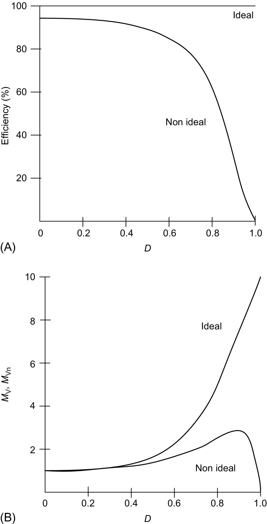
Efficiencies are usually specified in percent. Let us consider the boot converter as an example. Under low ripple assumption, the boost converter efficiency can be estimated as
η=R(1−D)2R(1−D)2(1+(VD/VO)+fCoR)+rL+DrS+(1−D)rD+D(1−D)rC

where VD is the forward conduction voltage drop of the diode, Co is the output capacitance of the switch, rL is the ESR of the inductor, and rD is the forward on resistance of the diode. The term fCoR in Eq. (10.38) represents switching losses in the converter. Other terms account for conduction losses. Losses in a dc-dc converter also contribute to a decrease in the dc voltage transfer function. The nonideal dc voltage transfer function MVn is a product of the ideal one and the efficiency:
MVn=ηMV
Sample graphs for the boost converter that correspond to Eqs. (10.38) and (10.39) are presented in Fig. 10.14.
10.8 Synchronous and Bidirectional Converters
It can be observed in Eq. (10.38) that the forward voltage of a diode VD contributes to a decrease in efficiency. This contribution is especially significant in low-output-voltage power supplies, for example, 3.3 V power supplies for microprocessors or power supplies for portable telecommunication equipment. Even with a Schottky diode, which has VD in the range of 0.4 V, the power loss in the diode can easily exceed 10% of the total power delivered to the load. To reduce conduction losses in the diode, a low on-resistance switch can be added in parallel as shown in Fig. 10.15 for a buck converter. The input switch and the switch parallel to the diode must be turned on and off alternately. The arrangement of Fig. 10.15 is called a synchronous converter or a synchronous rectifier. Modern low-voltage MOSFETs have on resistances of only several milliohms. Hence, a synchronous converter may exhibit higher efficiency than a conventional one at output currents as large as tens of amperes. The efficiency is increased at an expense of more complicated driving circuitry for the switches. In particular, a special can must be exercised to avoid having both switches on at the same time as this would short the input voltage source. Since power semiconductor devices usually have longer turn-off times than turn-on times, a dead time (sometimes called a blanking time) must be introduced in PWM driving signals.

The parallel combination of a controllable switch and a diode is also used in converters that allow for a current flow in both directions: from the input source to the load and from the load back to the input source. Such converters are called bidirectional power flow or simply bidirectional converters. As an example, a flyback bidirectional converter is shown in Fig. 10.16. It contains unipolar voltage and bidirectional current switch-diode combinations at both primary and secondary of the flyback transformer. When the primary switch and secondary diode operate, the current flows from the input source to the load. The converter current can also flow from the output to the input through the secondary switch and primary diode. Bidirectional arrangements can be made for buck and boost converters. A bidirectional buck converter operates as a boost converter when the current flow is from the output to the input. A bidirectional boost converter operates as a buck converter with a reversed current flow. If for any reason (for instance, to avoid the DCM) the controllable switches are driven at the same time, they must be driven alternately with a sufficient dead time to avoid a shot-through current.

10.9 Control Principles
A dc-dc converter must provide a regulated dc output voltage under varying load and input voltage conditions. The converter component values are also changing with time, temperature, pressure, etc. Hence, the control of the output voltage should be performed in a closed-loop manner using principles of negative feedback. Two most common closed-loop control methods for PWM dc-dc converters, namely, the voltage-mode control and the current-mode control, are presented schematically in Fig. 10.17.

In the voltage-mode control scheme shown in Fig. 10.17A, the converter output voltage is sensed and subtracted from an external reference voltage in an error amplifier. The error amplifier produces a control voltage that is compared to a constant-amplitude sawtooth waveform. The comparator produces a PWM signal that is fed to drivers of controllable switches in the dc-dc converter. The duty ratio of the PWM signal depends on the value of the control voltage. The frequency of the PWM signal is the same as the frequency of the sawtooth waveform. An important advantage of the voltage-mode control is its simple hardware implementation and flexibility.
The error amplifier in Fig. 10.17A reacts fast to changes in the converter output voltage. Thus, the voltage-mode control provides good load regulation, that is, regulation against variations in the load. Line regulation (regulation against variations in the input voltage) is, however, delayed because changes in the input voltage must first manifest themselves in the converter output before they can be corrected. To alleviate this problem, the voltage-mode control scheme is sometimes augmented by the so-called voltage feedforward path. The feedforward path affects directly the PWM duty ratio according to variations in the input voltage. As will be explained below, the input voltage feedforward is an inherent feature of current-mode control schemes.
The current-mode control scheme is presented in Fig. 10.17B. An additional inner control loop feeds back an inductor current signal. This current signal, converted into its voltage analog, is compared with the control voltage. This modification of replacing the sawtooth waveform of the voltage-mode control scheme by a converter current signal significantly alters the dynamic behavior of the converter. The converter takes on some characteristics of a current source. The output current in PWM dc-dc converters is either equal to the average value of the output inductor current (buck-derived and Ćuk converters) or a product of an average inductor current and a function of the duty ratio. In practical implementations of the current-mode control, it is feasible to sense the peak inductor current instead of the average value. Since the peak inductor current is equal to the peak switch current, the latter can be used in the inner loop, which often simplifies the current sensor. Note that the peak inductor (switch) current is proportional to the input voltage. Hence, the inner loop of the current-mode control naturally accomplishes the input voltage feedforward technique. Among several current-mode control versions, the most popular is the constant frequency one that requires a clock signal. Advantages of the current-mode control include input voltage feedforward, limit on the peak switch current, equal current sharing in modular converters, and reduction in the converter dynamic order. The main disadvantage of the current-mode control is its complicated hardware that includes a need to compensate the control voltage by ramp signals (to avoid converter instability).
Among other control methods of dc-dc converters, a hysteretic (or bang-bang) control is very simple for hardware implementation. The hysteretic control results, however, in variable frequency operation of semiconductor switches. Generally, a constant switching frequency is preferred in power electronic circuits for easier elimination of electromagnetic interference and better utilization of magnetic components.
Application-specific integrated circuits (ASICs) are commercially available that contain main elements of voltage- or current-mode control schemes. On a single 14- or 16-pin chip, there is error amplifier, comparator, sawtooth generator, or sensed current input, latch, and PWM drivers. The switching frequency is usually set by an external RC network and can be varied from tens of kilohertz to a few megahertz. The controller has an oscillator output for synchronization with other converters in modular power supply systems. A constant voltage reference is generated on the chip as well. Additionally, the ASIC controller may be equipped in various diagnostic and protection features: current limiting, overvoltage and undervoltage protection, soft start, dead time in case of multiple PWM outputs, and duty ratio limiting. In several dc-dc converter topologies, for example, buck and buck-boost, neither control terminal of semiconductor switches is grounded (so-called high-side switches). The ASIC controllers are usually designed for a particular topology, and their PWM drivers may be able to drive high-side switches in low-voltage applications. In high-voltage applications, external PWM drivers must be used. External PWM drivers are also used for switches with high input capacitances. To take a full advantage of the input-output isolation in transformer versions of dc-dc converters, such an isolation must be also provided in the control loop. Signal transformers or optocouplers are used for isolating feedback signals.
Dynamic characteristic of closed-loop dc-dc converters must fulfill certain requirements. To simple analysis, these requirements are usually translated into desired properties of the open loop. The open loop should provide a sufficient (typically, at least 45 degrees) phase margin for stability, high bandwidth (about one-tenth of the switching frequency) for good transient response, and high gain (several tens of decibels) at low frequencies for small steady-state error.
The open-loop dynamic characteristics are shaped by compensating networks of passive components around the error amplifier. Second- or third-order RC networks are commonly used. Since the converter itself is a part of the control loop, the design of compensating networks requires a knowledge of small-signal characteristics of the converter. There are several methods of small-signal characterization of PWM dc-dc converters. The most popular methods provide average models of converters under high-switching-frequency assumption. The averaged models are then linearized at an operating point to obtain small-signal transfer functions. Among analytic averaging methods, state-space averaging has been popular since the late 1970s. Circuit-based averaging is usually performed using PWM switch or direct replacement of semiconductor switches by controlled current and voltage sources. All these methods can take into account converter parasitics.
The most important small-signal characteristic is the control-to-output transfer function Tp. Other converter characteristics that are investigated include the input-to-output (or line-to-output) voltage transfer function, also called the open-loop dynamic line regulation or the audio susceptibility, which describes the input-output disturbance transmission; the open-loop input impedance; and the open-loop dynamic load regulation. Buck-derived, boost, and buck-boost converters are second-order dynamic systems; the Ćuk converter is a fourth-order system. Characteristics of buck and buck-derived converters are similar to each other. Another group of converters with similar small-signal characteristics is formed by boost, buck-boost, and flyback converters. Among parasitic components, the ESR of the filter capacitor rC introduces additional dynamic terms into transfer functions. Other parasitic resistances usually modify slightly the effective value of the load resistance. Sample characteristics below are given for nonzero rC, neglecting other parasitics.
The control-to-output transfer function of the forward converter is
Tp(s)≡vo(s)d(s)|vs(s)=0=VIRrCnL(R+rC)×s+(1/CrC)s2+s(CRrC+L/LC(R+rC))+R/(LC(R+rC))
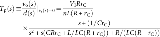
It can be seen that this transfer function has two poles and one zero. The zero is due to the filter capacitor ESR. Buck-derived converters can be easily compensated for stability with second-order controllers.
The control-to-output transfer function of the boost converter is given by
Tp(s)=−VOrC(1−D)(R+rC)×[s+(1/CrC)][s−((1−D)2R)/L]s2+s[((1−D)2CRrC+L)/(LC(R+rC))]+[((1−D)2R)/(LC(R+rC))]
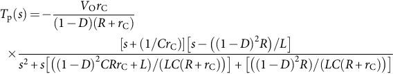
The zero −(1−D)2R/L is located in the right half of the s-plane. Therefore, the boost converter (and buck-boost and flyback converters) is a nonminimum phase system. Nonminimum phase dc-dc converters are typically compensated with third-order controllers. Step-by-step procedures for a design of compensating networks are usually given by manufacturers of ASIC controllers in application notes.
The final word of this section is on the behavior of dc-dc converters in distributed power supply systems. An important feature of closed-loop regulated dc-dc converters is that they exhibit a negative input resistance. As the load voltage is kept constant by the controller, the output power changes with the load. With slow load changes, an increase (decrease) in the input voltage results in a decrease (increase) in the input power. This negative resistance property must be carefully examined during the system design to avoid resonances.
10.10 Applications of DC-DC Converters
Step-down choppers find most of their applications in high-performance dc drive systems, for example, electric traction, electric vehicles, and machine tools. The dc motors with their winding inductances and mechanical inertia act as filters resulting in high-quality armature currents. The average output voltage of step-down choppers is a linear function of the switch duty ratio. Step-up choppers are used primarily in radar and ignition systems. The dc choppers can be modified for two-quadrant and four-quadrant operation. Two-quadrant choppers may be a part of autonomous power supply system that contain battery packs and such renewable dc sources as photovoltaic arrays, fuel cells, or wind turbines. Four-quadrant choppers are applied in drives in which regenerative breaking of dc motors is desired, for example, transportation systems with frequent stops. The dc choppers with inductive outputs serve as inputs to current-driven inverters.
An addition of filtering reactive components to dc choppers results in PWM dc-dc converters. The dc-dc converters can be viewed as dc transformers that deliver to the load as dc voltage or current at a different level than the input source. This dc transformation is performed by electronic switching means, not by electromagnetic means like in conventional transformers. Output voltages of dc-dc converters range from a volt for special VLSI circuits to tens of kilovolts in x-ray lamps. The most common output voltages are 3.3 V for modern microprocessors, 5 and 12 V for logic circuits, 48 V for telecommunication equipment, and 270 V for main dc bus on airplanes. Typical input voltages include 48, 170 (the peak value of a 120 V rms line), and 270 V.
Selection of a topology of dc-dc converters is determined not only by input/output voltages, which can be additionally adjusted with the turns ratio in isolated converters, but also by power levels, voltage and current stresses of semiconductor switches, and utilization of magnetic components. The low part-count flyback converter is popular in low-power applications (up to 200 W). Its main deficiencies are the large size of the flyback transformer core and high voltage stress on the semiconductor switch. The forward converter is also a single-switch converter. Since its core size requirements are smaller, it is popular in low-/medium (up to several hundreds of watts)-power applications. Disadvantages of the forward converter are in a need for demagnetizing winding and in a high voltage stress on the semiconductor switch. The push-pull converter is also used at medium power levels. Due to bidirectional excitation, the transformer size is small. An advantage of the push-pull converter is also a possibility to refer driving terminals of both switches to the ground, which greatly simplifies the control circuitry. A disadvantage of the push-pull converter is a potential core saturation in a case of asymmetry. The half-bridge converter has similar range of applications as the push-pull converter. There is no danger of transformer saturation in the half-bridge converter. It requires, however, two additional input capacitors to split in half the input dc source. The full-bridge converter is used at high (several kilowatts) power and voltage levels. The voltage stress on power switches is limited to the input voltage source value. A disadvantage of the full-bridge converter is a high number of semiconductor devices.
The dc-dc converters are building blocks of distributed power supply systems in which a common dc bus voltage is converted to various other voltages according to the requirements of particular loads. Such distributed dc systems are common in space stations, ships, and airplanes, as well as in computer and telecommunication equipment. It is expected that modern portable wireless communication and signal processing systems will use variable supply voltages to minimize power consumption and extend battery life. Low-output-voltage converters in these applications utilize the synchronous rectification arrangement.
Another big area of dc-dc converter applications is related to the utility ac grid. For critical loads, if the utility grid fails, there must be a backup source of energy, for example, a battery pack. This need for continuous power delivery gave rise to various types of uninterruptible power supplies (UPSs). The dc-dc converters are used in UPSs to adjust the level of a rectified grid voltage to that of the backup source. Since during normal operation the energy flows from the grid to the backup source and during emergency conditions the backup source must supply the load, bidirectional dc-dc converters are often used. The dc-dc converters are also used in dedicated battery chargers.
Power electronic loads, especially those with front-end rectifiers, pollute the ac grid with odd harmonics. The dc-dc converters are used as intermediate stages, just after a rectifier and before the load-supplying dc-dc converter, for shaping the input ac current to improve power factor and decrease the harmonic content. The boost converter is especially popular in such power-factor-correction (PFC) applications. Another utility grid-related application of dc-dc converters is in interfaces between ac networks and dc renewable energy sources such as fuel cells and photovoltaic arrays.
In isolated dc-dc converters, multiple outputs are possible with additional secondary windings of transformers. Only one output is regulated with a feedback loop. Other outputs depend on the duty ratio of the regulated one and on their loads. A multiple-output dc-dc converter is a convenient solution in application where there is a need for one closely regulated output voltage and for one or more noncritical other output voltage levels.