
Power Supplies
Yuk M. Lai The Hong Kong Polytechnic University, Kowloon, Hong Kong
Keywords
Power supplies; Linear regulators; Switching regulators; Pulse-width modulation
20.1 Introduction
Power supplies are used in most electric equipment. Their applications cut across a wide spectrum of product types, ranging from consumer appliances to industrial utilities, from milliwatts to megawatts, and from handheld tools to satellite communications.
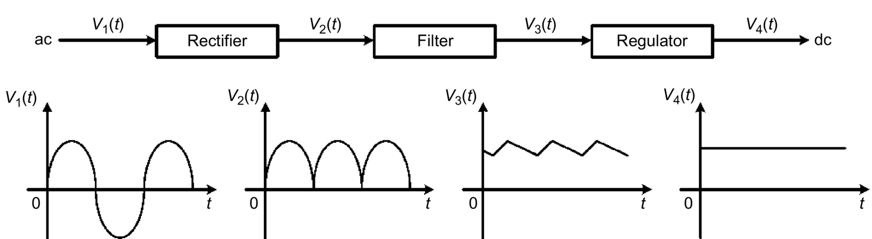
By definition, a power supply is a device that converts the output from an ac power line to a steady dc output or multiple outputs. The ac voltage is first rectified to provide a pulsating dc and then filtered to produce a smooth voltage. Finally, the voltage is regulated to produce a constant output level despite variations in the ac line voltage or circuit loading. Fig. 20.1 illustrates the process of rectification, filtering, and regulation in a dc power supply. The transformer, rectifier, and filtering circuits are discussed in other chapters. In this chapter, we will concentrate on the operation and characteristics of the regulator stage of a dc power supply.
In general, the regulator stage of a dc power supply consists of a feedback circuit, a stable reference voltage, and a control circuit to drive a pass element (a solid-state device such as transistor and MOSFET). The regulation is done by sensing variations appearing at the output of the dc power supply. A control signal is produced to drive the pass element to cancel any variation. As a result, the output of the dc power supply is maintained essentially constant. In a transistor regulator, the pass element is a transistor, which can be operated in its active region or as a switch, to regulate the output voltage. When the transistor operates at any point in its active region, the regulator is referred to as a linear voltage regulator. When the transistor operates only at cutoff and at saturation, the circuit is referred to as a switching regulator.
Linear voltage regulators can be further classified as either series or shunt types. In a series regulator, the pass transistor is connected in series with the load as shown in Fig. 20.2. Regulation is achieved by sensing a portion of the output voltage through the voltage divider network R1 and R2 and comparing this voltage with the reference voltage VREF to produce a resulting error signal that is used to control the conduction of the pass transistor. This way, the voltage drop across the pass transistor is varied and the output voltage delivered to the load circuit is essentially maintained constant.

In the shunt regulator shown in Fig. 20.3, the pass transistor is connected in parallel with the load, and a voltage-dropping resistor R3 is connected in series with the load. Regulation is achieved by controlling the current conduction of the pass transistor such that the current through R3 remains essentially constant. This way, the current through the pass transistor is varied, and the voltage across the load remains constant.

As opposed to linear voltage regulators, switching regulators employ solid-state devices, which operate as switches: either completely on or completely off, to perform power conversion. Because the switching devices are not required to operate in their active regions, switching regulators enjoy a much lower power loss than those of linear voltage regulators. Fig. 20.4 shows a switching regulator in a simplified form. The high-frequency switch converts the unregulated dc voltage from one level to another dc level at an adjustable duty cycle. The output of the dc supply is regulated by means of a feedback control that employs a pulse-width modulator (PWM) controller, where the control voltage is used to adjust the duty cycle of the switch.

Both linear and switching regulators are capable of performing the same function of converting an unregulated input into a regulated output. However, these two types of regulators have significant differences in properties and performances. In designing power supplies, the choice of using certain type of regulator in a particular design is significantly based on the cost and performance of the regulator itself. In order to use the more appropriate regulator type in the design, it is necessary to understand the requirements of the application and select the type of regulator that best satisfies those requirements. Advantages and disadvantages of linear regulators, as compared with switching regulators, are given below:
1. Linear regulators exhibit efficiency of 20%–60%, whereas switching regulators have a much higher efficiency, typically 70%–95%.
2. Linear regulators can only be used as a step-down regulator, whereas switching regulators can be used in both step-up and step-down operations.
3. Linear regulators require a mains frequency transformer for off-the-line operation. Therefore, they are heavy and bulky. On the other hand, switching regulators use high-frequency transformers and can therefore be small in size.
4. Linear regulators generate little or no electric noise at their outputs, whereas switching regulators may produce considerable noise if they are not properly designed.
5. Linear regulators are more suitable for applications of less than 20 W, whereas switching regulators are more suitable for large-power applications.
In this chapter, we will examine the circuit operation, characteristics, and applications of linear and switching regulators. In Section 20.2, we will look at the basic circuits and properties of linear series voltage regulators. Some current-limiting techniques will be explained. In Section 20.3, linear shunt regulators will be covered. The important characteristics and uses of linear integrated circuit (IC) regulators will be discussed in Section 20.4. Finally, the operation and characteristics of switching regulators will be discussed in Section 20.5. Important design guidelines for switching regulators will also be given in this section.
20.2 Linear Series Voltage Regulator
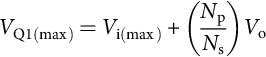
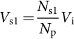
A zener diode regulator can maintain a fairly constant voltage across a load resistor. It can be used to improve the voltage regulation and reduce the ripple in a power supply. However, the regulation is poor, and the efficiency is low because of the nonzero resistance in the zener diode. To improve the regulation and efficiency of the regulator, we have to limit the zener current to a smaller value. This can be accomplished by using an amplifier in series with the load as shown in Fig. 20.5. The effect of this amplifier is to limit the variation of the current ID through the zener diode Dz. This circuit is known as a linear series voltage regulator because the transistor is in series with the load.
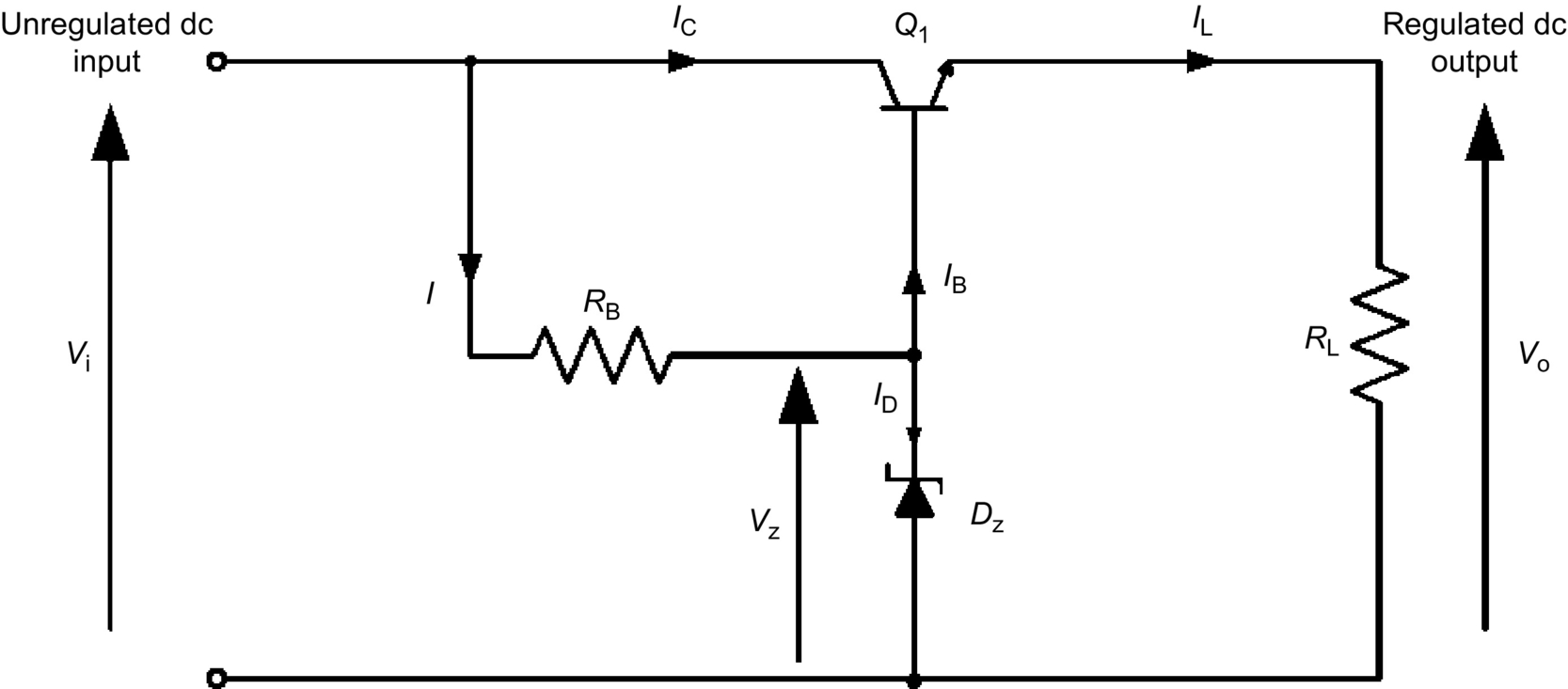
Because of the current-amplifying property of the transistor, ID is reduced by a factor of ![]() , where β is the dc current gain of the transistor. Hence, there is a small voltage drop across the diode resistance, and the zener diode approximates an ideal voltage source. The output voltage Vo of the regulator is
, where β is the dc current gain of the transistor. Hence, there is a small voltage drop across the diode resistance, and the zener diode approximates an ideal voltage source. The output voltage Vo of the regulator is
where Vz is the zener voltage and VBE is the base-to-emitter voltage of the transistor. The change in output voltage is
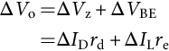
where rd is the dynamic resistance of the zener diode and re is the output resistance of the transistor. Assume that Vi and Vz are constant. With ![]() , the change in output voltage is then
, the change in output voltage is then
If Vi is not constant, then the current I will change with the input voltage. In calculating the change in output voltage, this current change must be absorbed by the zener diode.
In designing linear series voltage regulators, it is imperative that the series transistor must work within the rated safe operation area (SOA) and be protected from excess heat dissipation because of current overload. The emitter-to-collector voltage VCE of Q1 is given by
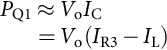
Thus, with specified output voltage, the maximum allowable VCE for a given Q1 is determined by the maximum input voltage to the regulator. The power dissipated by Q1 can be approximated by
Consequently, the maximum allowable power dissipated in Q1 is determined by the combination of the input voltage Vi and the load current IL of the regulator. For a low output voltage and a high loading current regulator, the power dissipated in the series transistor is about 50% of the power delivered to the output.
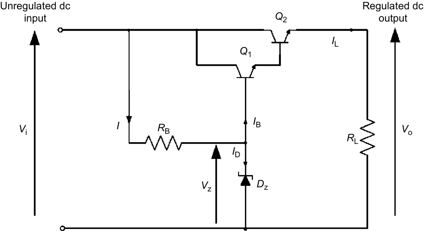
In many high-current high-voltage regulator circuits, it is necessary to use a Darlington-connected transistor pair so that the voltage, current, and power ratings of the series element are not exceeded. The method is shown in Fig. 20.6. An additional desirable feature of this circuit is that the reference diode dissipation can be reduced greatly. The maximum base current IB1 is then ![]() , where β1 and β2 are the dc current gain of Q1 and Q2, respectively. This current is usually of the order of less than 1 mA. Consequently, a low-power reference diode can be used.
, where β1 and β2 are the dc current gain of Q1 and Q2, respectively. This current is usually of the order of less than 1 mA. Consequently, a low-power reference diode can be used.
20.2.1 Regulating Control
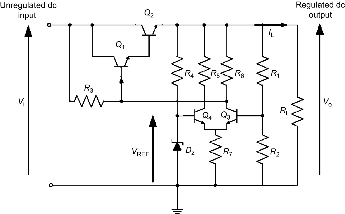
The series regulators shown in Figs. 20.5 and 20.6 do not have feedback loop. Although they provide satisfactory performance for many applications, their output resistances and ripples cannot be reduced. Fig. 20.7 shows an improved form of the series regulator, in which negative feedback is employed to improve the performance. In this circuit, transistors Q3 and Q4 form a single-ended differential amplifier, and the gain of this amplifier is established by R6. Here, Dz is a stable zener diode reference, biased by R4. For higher accuracy, Dz can be replaced by an IC reference such as REF series from Burr-Brown. Resistors R1 and R2 form a voltage divider for output voltage sensing. Finally, transistors Q1 and Q2 form a Darlington pair output stage. The operation of the regulator can be explained as follows. When Q1 and Q2 are on, the output voltage increases, and hence, the voltage VA at the base of Q3 also increases. During this time, Q3 is off and Q4 is on. When VA reaches a level that is equal to the reference voltage VREF at the base of Q4, the base-emitter junction of Q3 becomes forward-biased. Some Q1 base current will divert into the collector of Q3. If the output voltage Vo starts to rise above VREF, Q3 conduction increases to further decrease the conduction of Q1 and Q2, which will in turn maintain output voltage regulation. Fig. 20.8 shows another improved series regulator that uses an operational amplifier to control the conduction of the pass transistor.

One of the problems in the design of linear series voltage regulators is the high-power dissipation in the pass transistors. If an excess load current is drawn, the pass transistor can be quickly damaged or destroyed. In fact, under short-circuit conditions, the voltage across Q2 in Fig. 20.7 will be the input voltage Vi, and the current through Q2 will be greater than the rated full-load output current. This current will cause Q1 to exceed its rated SOA unless the current is reduced. In the next section, some current-limiting techniques will be presented to overcome this problem.
20.2.2 Current Limiting and Overload Protection
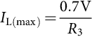
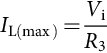
In some series voltage regulators, overloading causes permanent damage to the pass transistors. The pass transistors must be kept from excessive power dissipation under current overloads or short-circuit conditions. A current-limiting mechanism must be used to keep the current through the transistors at a safe value as determined by the power rating of the transistors. The mechanism must be able to respond quickly to protect the transistor and yet permit the regulator to return to normal operation as soon as the overload condition is removed. One of the current-limiting techniques to prevent current overload, called the constant current-limiting method, is shown in Fig. 20.9A. Current limiting is achieved by the combined action of the components shown inside the dashed line. The voltage developed across the current-limit resistor R3 and the base-to-emitter voltage of current-limit transistor Q3 is proportional to the circuit output current IL. During current overload, IL reaches a predetermined maximum value that is set by the value of R3 to cause Q3 to conduct. As Q3 starts to conduct, Q3 shunts a portion of the Q1 base current. This action, in turn, decreases and limits IL to a maximum value IL(max). Since the base-to-emitter voltage VBE of Q3 cannot exceed above 0.7 V, the voltage across R3 is held at this value and IL(max) is limited to
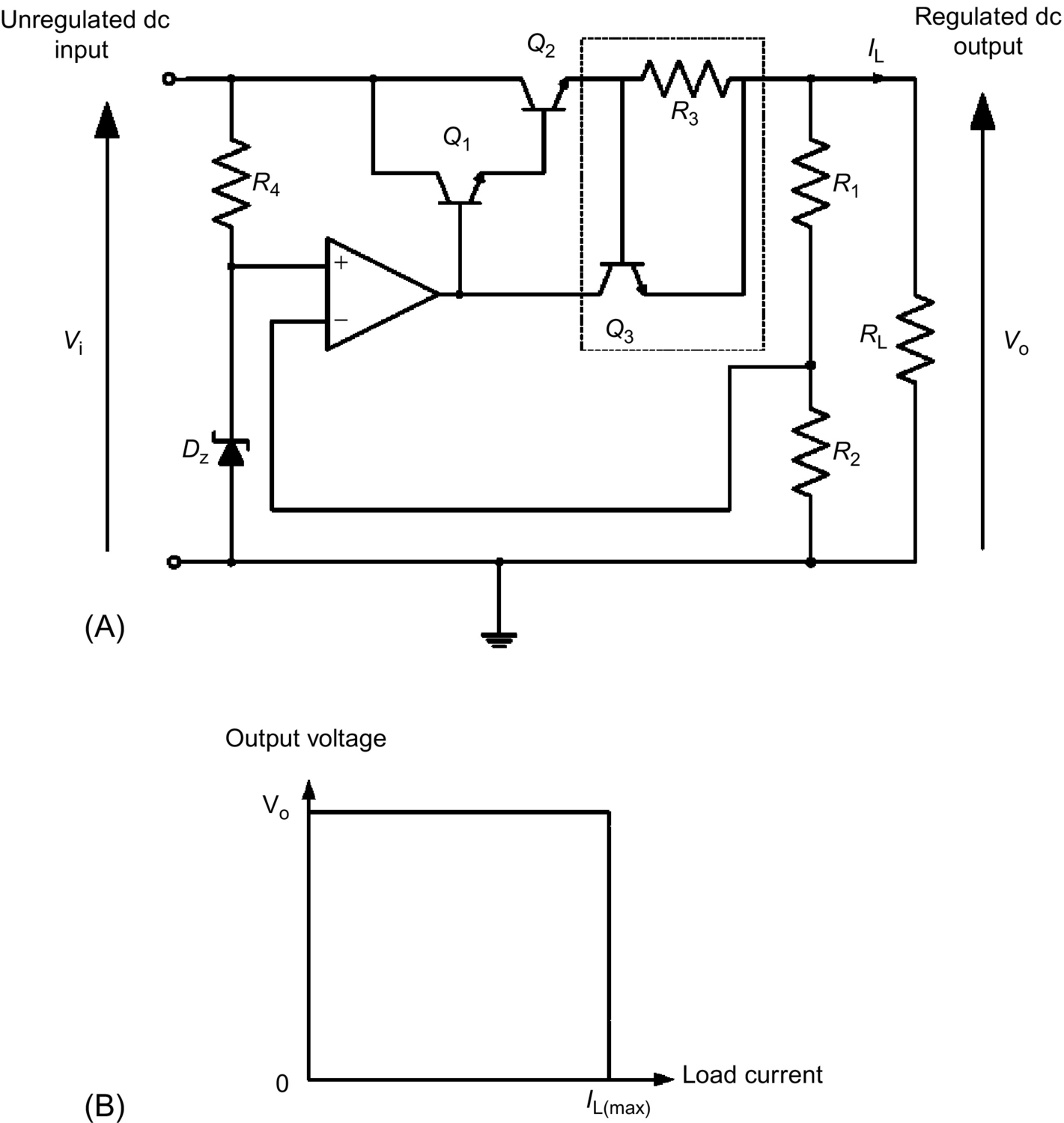
Consequently, the value of the short-circuit current is selected by adjusting the value of R3. The voltage-current characteristic of this circuit is shown in Fig. 20.9B.
In many high-current regulators, foldback current limiting is always used to protect against excessive current. This technique is similar to the constant current-limiting method, except that as the output voltage is reduced as a result of load impedance moving toward zero, the load current is also reduced. Therefore, a series voltage regulator that includes a foldback current-limiting circuit has the voltage-current characteristic shown in Fig. 20.10. The basic idea of foldback current limiting, with reference to Fig. 20.11, can be explained as follows. The foldback current-limiting circuit (in dashed outline) is similar to the constant current-limiting circuit, with the exception of resistors R5 and R6. At low output current, the current-limit transistor Q3 is cutoff.
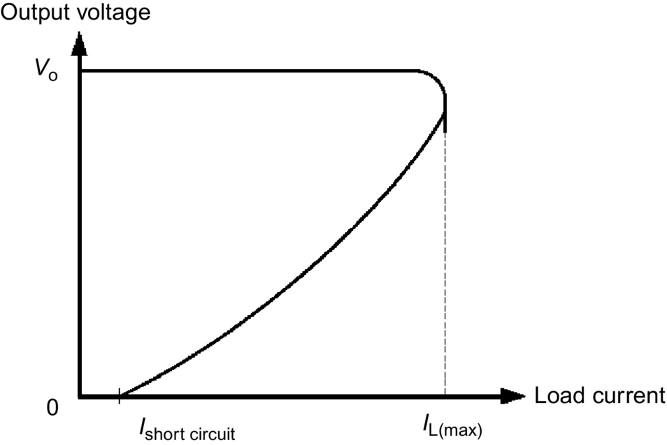

A voltage proportional to the output current IL is developed across the current-limit resistor R3. This voltage is applied to the base of Q3 through the divider network R5 and R6. At the point of transition into current limit, any further increase in IL will increase the voltage across R3 and hence across R5, and Q3 will progressively be turned on. As Q1 conducts, it shunts a portion of the Q1 base current. This action, in turn, causes the output voltage to fall. As the output voltage falls, the voltage across R6 decreases and the current in R6 also decreases, and more current is shunted into the base of Q3. Hence, the current required in R3 to maintain the conduction state of Q3 is also decreased. Consequently, as the load resistance is reduced, the output voltage and current fall, and the current-limit point decreases toward a minimum when the output voltage is short-circuited. In summary, any regulator using foldback current limiting can have peak load current up to IL(max). But when the output becomes shorted, the current drops to a lower value to prevent overheating of the series transistors.
20.3 Linear Shunt Voltage Regulator
The second type of linear voltage regulator is the shunt regulator. In the basic circuit shown in Fig. 20.12, the pass transistor Q1 is connected in parallel with the load. A voltage-dropping resistor R3 is in series with this parallel network. The operation of the circuit is similar to that of the series regulator, except that regulation is achieved by controlling the current through Q1. The operation of the circuit can be explained as follows. When the output voltage tries to increase because of a change in load resistance, the voltage at the noninverting terminal of the operational amplifier also increases. This voltage is compared with a reference voltage, and the resulting difference voltage causes Q1 conduction to increase. With constant Vi and Vo, IL will decrease, and Vo will remain constant. The opposite action occurs when Vo tries to decrease. The voltage appearing at the base of Q1 causes its conduction to decrease. This action offsets the attempted decrease in Vo and maintains it at an almost constant level.

Analytically, the current flowing in R3 is
and

With IL and Vo constant, a change in Vi will cause a change in ![]() :
:

With Vi and Vo constant,
Eq. (20.10) shows that if IQ1 increases, IL decreases and vice versa. Although shunt regulators are not as efficient as series regulators for most applications, they have the advantage of greater simplicity. This topology offers inherently short-circuit protection. If the output is shorted, the load current is limited by the series resistor R3 and is given by
The power dissipated by Q1 can be approximated by
For a low value of IL, the power dissipated in Q1 is large, and the efficiency of the regulator may drop to 10% under this condition.
To improve the power handling of the shunt transistor, one or more transistors connected in the common-emitter configuration in parallel with the load can be employed, as shown in Fig. 20.13.

20.4 Integrated Circuit Voltage Regulators
The linear series and shunt voltage regulators presented in the previous sections have been developed by various solid-state device manufacturers and are available in integrated circuit (IC) form. Like discrete voltage regulators, linear IC voltage regulators maintain an output voltage at a constant value despite variations in load and input voltage.
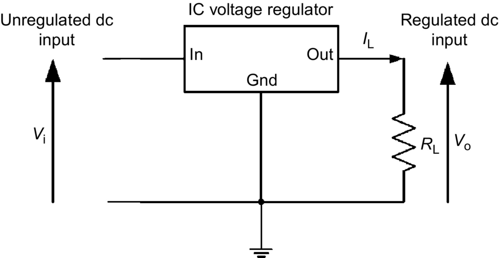
In general, linear IC voltage regulators are three-terminal devices that provide regulation of a fixed positive voltage, a fixed negative voltage, or an adjustable set voltage. The basic connection of a three-terminal IC voltage regulator to a load is shown in Fig. 20.14. The IC regulator has an unregulated input voltage Vi applied to the input terminals, a regulated voltage Vo at the output, and a ground connected to the third terminal. Depending on the selected IC regulator, the circuit can be operated with load currents ranging from milliamperes to tens of amperes and output power from milliwatts to tens of watts. Note that the internal construction of IC voltage regulators may be somewhat more complex and different from that previously described for discrete voltage regulator circuits. However, the external operation is much the same. In this section, some typical linear IC regulators are presented, and their applications are also given.
20.4.1 Fixed Positive and Negative Linear Voltage Regulators
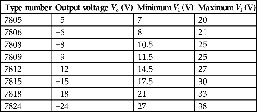
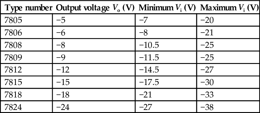
The 78XX series of regulators provide fixed regulated voltages from 5 to 24 V. The last two digits of the IC part number denote the output voltage of the device. For example, a 7824 IC regulator produces a +24 V regulated voltage at the output. The standard configuration of a 78XX fixed positive voltage regulator is shown in Fig. 20.15. The input capacitor C1 acts as a line filter to prevent unwanted variations in the input line, and the output capacitor C2 is used to filter the high-frequency noise that may appear at the output. In order to ensure proper operation, the input voltage of the regulator must be at least 2 V above the output voltage. Table 20.1 shows the minimum and maximum input voltages of the 78XX series fixed positive voltage regulator.

Table 20.1
Minimum and maximum input voltages for 78XX series regulators
| Type number | Output voltage Vo (V) | Minimum Vi (V) | Maximum Vi (V) |
| 7805 | +5 | 7 | 20 |
| 7806 | +6 | 8 | 21 |
| 7808 | +8 | 10.5 | 25 |
| 7809 | +9 | 11.5 | 25 |
| 7812 | +12 | 14.5 | 27 |
| 7815 | +15 | 17.5 | 30 |
| 7818 | +18 | 21 | 33 |
| 7824 | +24 | 27 | 38 |
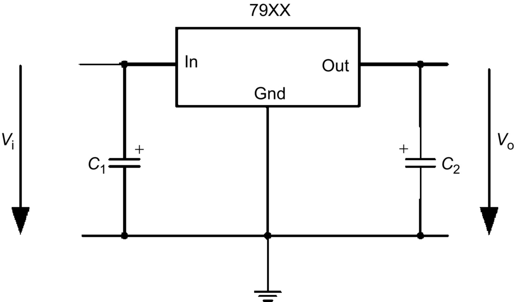
The 79XX series voltage regulator is identical to the 78XX series except that it provides negative regulated voltages instead of positive ones. Fig. 20.16 shows the standard configuration of a 79XX series voltage regulator. A list of 79XX series regulators is provided in Table 20.2. The regulation of the circuit can be maintained as long as the output voltage is at least 2–3 V greater than the input voltage.
20.4.2 Adjustable Positive and Negative Linear Voltage Regulators
The IC voltage regulators are also available in circuit configurations that allow the user to set the output voltage to a desired regulated value. The LM317 adjustable positive voltage regulator, for example, is capable of supplying an output current of more than 1.5 A over an output voltage range of 1.2–37 V. Fig. 20.17 shows how the output voltage of an LM317 can be adjusted by using two external resistors R1 and R2. The capacitors C1 and C2 have the same function as those in the fixed linear voltage regulator.

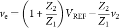
As indicated in Fig. 20.17, the LM317 has a constant 1.25 V reference voltage, VREF, across the output and the adjustment terminals. This constant reference voltage produces a constant current through R1 regardless of the value of R2. The output voltage Vo is given by

where Iadj is a constant current into the adjustment terminal and has a value of approximately 50 μA for the LM317. As can be seen from Eq. (20.13), with fixed R1, Vo can be adjusted by varying R2.
The LM337 adjustable voltage regulator is similar to the LM317 except that it provides negative regulated voltages instead of positive ones. Fig. 20.18 shows the standard configuration of an LM337 voltage regulator. The output voltage can be adjusted from −1.2 to −37 V, depending on the external resistors R1 and R2.

20.4.3 Applications of Linear IC Voltage Regulators
Most IC regulators are limited to an output current of 2.5 A. If the output current of an IC regulator exceeds its maximum allowable limit, its internal pass transistor will dissipate an amount of energy more than it can tolerate. As a result, the regulator will be shutdown.
For applications that require more than the maximum allowable current limit of a regulator, an external pass transistor can be used to increase the output current. Fig. 20.19 illustrates such a configuration. This circuit has the capability of producing higher current to the load but still preserving the thermal shutdown and short-circuit protection of the IC regulator.
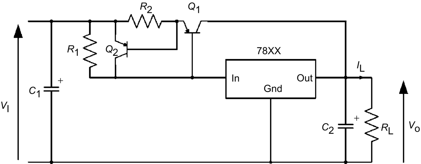
A constant current-limiting scheme, as discussed in Section 20.2.2, is implemented by using the transistor Q2 and the resistor R2 to protect the external pass transistor Q1 from excessive current under current-overload or short-circuit conditions. The value of the external current-sensing resistor R1 determines the value of current at which Q1 begins to conduct. As long as the current is less than the value set by R1, the transistor Q1 is off, and the regulator operates normally as shown in Fig. 20.15. But when the load current IL starts to increase, the voltage across R1 also increases. This turns on the external transistor Q1 and conducts the excess current. The value of R1 is determined by

where Imax is the maximum current that the voltage regulator can handle internally.
20.5 Switching Regulators
The linear series and shunt regulators have control transistors that are operating in their linear active regions. Regulation is achieved by varying the conduction of the transistors to maintain the output voltage at a desirable level. The switching regulator is different in that the control transistor operates as a switch, either in cutoff or saturation region. Regulation is achieved by adjusting the on-time of the control transistor. In this mode of operation, the control transistor does not dissipate as much power as that in the linear types. Therefore, switching voltage regulators have a much higher efficiency and can provide greater load currents at low voltage than linear regulators.
Unlike their linear counterparts, switching regulators can be implemented by many different topologies such as forward and flyback. In order to select an appropriate topology for an application, it is necessary to understand the merits and drawbacks of each topology and the requirements of the application. Basically, most topologies can work for various applications. Therefore, we have to determine from the factors such as cost, performances, and application that make one topology more desirable than the others. However, no matter which topology we decide to use, the basic building blocks of an off-the-line switching power supply are the same, as depicted in Fig. 20.1.
In this section, some popular switching regulator topologies, namely, flyback, forward, half-bridge, and full-bridge topologies, are presented. Their basic operation is described, and the critical waveforms are shown and explained. The merits, drawbacks, and application areas of each topology are discussed. Finally, the control circuitry and PWM of the regulators will also be discussed.
20.5.1 Single-Ended Isolated Flyback Regulators
An isolated flyback regulator consists of four main circuit elements: a power switch, a rectifier diode, a transformer, and a filter capacitor. The power switch, which can be either a power transistor or a MOSFET, is used to control the flow of energy in the circuit. A transformer is placed between the input source and the power switch to provide dc isolation between the input and the output circuits. In addition to being an energy storage element, the transformer also performs a stepping up or down function for the regulator. The rectifier diode and filter capacitor form an energy transfer mechanism to supply energy to maintain the output voltage of the supply. Note that there are two distinct operating modes for flyback regulators: continuous and discontinuous. However, both modes have an identical circuit. It is only the transformer magnetizing current that determines the operating mode of the regulator. Fig. 20.20A shows a simplified isolated flyback regulator. The associated steady-state waveforms, resulting from a discontinuous-mode operation, are shown in Fig. 20.20B. As shown in the figure, the voltage regulation of the regulator is achieved by a control circuit, which controls the conduction period or duty cycle of the switch, to keep the output voltage at a constant level. For clarity, the schematics and operation of the control circuit will be discussed in a separate section.
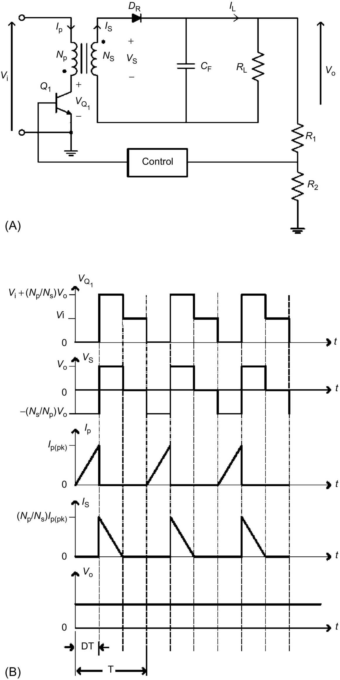
20.5.1.1 Discontinuous-Mode Flyback Regulators
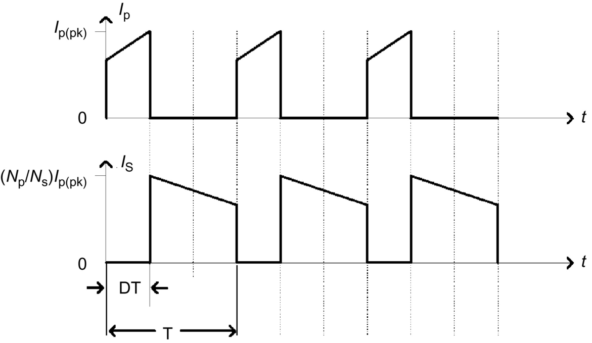
Under steady-state conditions, the operation of the regulator can be explained as follows. When the power switch Q1 is on, the primary current Ip starts to build up and stores energy in the primary winding. Because of the opposite polarity arrangement between the input and output windings of the transformer, the rectifier diode DR is reverse-biased. In this period of time, there is no energy transferred from the input to the load RL. The output voltage is supported by the load current IL, which is supplied from the output filter capacitor CF. When Q1 is turned off, the polarity of the windings reverses as a result of the fact that Ip cannot change instantaneously. This causes DR to turn on. Now, DR is conducting, charging the output capacitor CF, and delivering current to RL. This charging action ends at the point where all the magnetic energy stored in the secondary winding during the first half cycle is emptied. At this point, DR will cease to conduct and RL absorbs energy just from CF until Q1 is switched on again.
During the Q1 on-time, the voltage across the primary winding of the transformer is Vi. The current in the primary winding Ip increases linearly and is given by

where Lp is the primary magnetizing inductance. At the end of the on-time, the primary current reaches a value equal to Ip(pk) and is given by
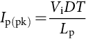
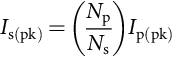
where D is the duty cycle and T is the switching period. Now, when Q1 turns off, the magnetizing current in the transformer forces the reversal of polarities on the windings. At the instant of turnoff, the amplitude of the secondary current Is(pk) is
This current decreases linearly at the rate of

where Ls is the secondary magnetizing inductance.
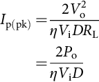
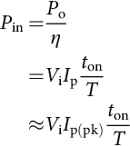
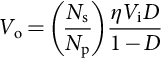
In the discontinuous-mode operation, Is(pk) will decrease linearly to zero before the start of the next cycle. Since the energy transfer from the source to the output takes place only in the first half cycle, the power drawn from Vi is then

Substituting Eq. (20.15) into Eq. (20.19), we have

The output power Po may be written as
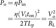
where η is the efficiency of the regulator. Then, from Eq. (20.21), the output voltage Vo is related to the input voltage Vi by
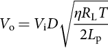
Since the collector voltage VQ1 of Q1 is maximum when Vi is maximum, the maximum collector voltage VQ1(max), as shown in Fig. 20.20B, is given by
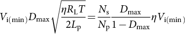
The primary peak current Ip(pk) can be found in terms of Po by combining Eq. (20.16) and Eq. (20.21) and then eliminating Lp as
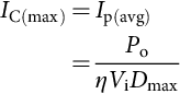
The maximum collector current IC(max) of the power switch Q1 at turn on is
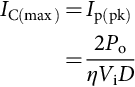
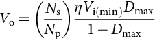
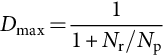
As can be seen from Eq. (20.21), Vo will be maintained constant by keeping the product Viton constant. Since maximum on-time ton(max) occurs at minimum supply voltage Vi(min), the maximum allowable duty cycle for the discontinuous mode can be found from Eq. (20.22) as
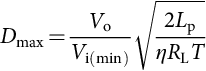
and Vo at Dmax is then

20.5.1.2 Continuous-Mode Flyback Regulators
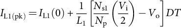
In the continuous-mode operation, the power switch is turned on before all the magnetic energy stored in the secondary winding empties itself. The primary and secondary current waveforms have a characteristic appearance as shown in Fig. 20.21. This mode produces a higher-power capability without increasing the peak currents. During the on-time, the primary current Ip rises linearly from its initial value Ip(0) and is given by
At the end of the on-time, the primary current reaches a value equal to Ip(pk) and is given by

In general, ![]() ; thus, Eq. (20.29) can be written as
; thus, Eq. (20.29) can be written as
The secondary current Is at the instant of turn off is given by

This current decreases linearly at the rate of
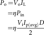
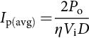
The output power Po is equal to Vo times the time average of the secondary current pulses and is given by
or
For an efficiency of η, the input power Pin is
or

Combining Eqs. (20.31), (20.34), and (20.36) and solving for Vo, we have
The output voltage at Dmax is then
The maximum collector current IC(max) for the continuous mode is then given by

The maximum collector voltage of Q1 is the same as that in the discontinuous mode and is given by
The maximum allowable duty cycle for the continuous mode can be found from Eq. (20.38) and is given by

At the transition from the discontinuous mode to continuous mode (or from continuous mode to discontinuous mode), the relationships in Eqs. (20.27) and (20.38) must hold. Thus, equating these two equations, we have
Solving this equation for Lp to give the critical inductance ![]() , at which the transition occurs, we have
, at which the transition occurs, we have

Replacing Vo with Eq. (20.38) and solving for Lp(limit), we have

Then, for a given Dmax, input, and output quantities, the inductance value Lp(limit) in Eq. (20.44) determines the mode of operation for the regulator. If ![]() , then the circuit is operated in the discontinuous mode. Otherwise, if
, then the circuit is operated in the discontinuous mode. Otherwise, if ![]() , the circuit is operated in the continuous mode.
, the circuit is operated in the continuous mode.
In designing flyback regulators, regardless of their operating modes, the power switch must be able to handle the peak collector voltage at turnoff and the peak collector currents at turn-on as shown in Eqs. (20.23), (20.25), (20.39), and (20.40). The flyback transformer, because of its unidirectional use of the B-H curve, has to be designed so that it will not be driven into saturation. To avoid saturation, the transformer needs a relatively large core with an air gap in it.
Although the continuous and discontinuous modes have an identical circuit, their operating properties differ significantly. As opposed to the discontinuous mode, the continuous mode can provide higher-power capability without increasing the peak current Ip(pk). It means that, for the same output power, the peak currents in the discontinuous mode are much higher than those operated in the continuous mode. As a result, a higher current rating and, therefore, a more expensive power transistor are needed. Moreover, the higher secondary peak currents in the discontinuous mode will have a larger transient spike at the instant of turnoff. However, despite all these problems, the discontinuous mode is still much more widely used than its continuous-mode counterpart. There are two main reasons. First, the inherently smaller magnetizing inductance gives the discontinuous mode a quicker response and a lower transient output voltage spike to sudden changes in load current or input voltage. Second, the continuous mode has a right-half-plane zero in its transfer function, which makes the feedback control circuit more difficult to design.
The flyback configuration is mostly used in applications with output power below 100 W. It is widely used for high output voltages at relatively low power. The essential attractions of this configuration are its simplicity and low cost. Since no output filter inductor is required for the secondary, there is a significant saving in cost and space, especially for multiple output power supplies. Since there is no output filter inductor, the flyback exhibits high ripple currents in the transformer and at the output. Thus, for higher-power applications, the flyback becomes an unsuitable choice. In practice, a small LC filter is added after the filter capacitor CF in order to suppress high-frequency switching noise spikes.
As mentioned previously, the collector voltage of the power transistor must be able to sustain a voltage as defined in Eq. (20.23). In cases where the voltage is too high for the transistor to handle, the double-ended flyback regulator shown in Fig. 20.22 may be used. The regulator uses two transistors that are switched on or off simultaneously. The diodes DR1 and DR2 are used to restrict the maximum collector voltage to Vi. Therefore, the transistors with a lower voltage rating can be used in the circuit.

20.5.2 Single-Ended Isolated Forward Regulators
Although the general appearance of an isolated forward regulator resembles that of its flyback counterpart, their operations are different. The key difference is that the dot on the secondary winding of the transformer is so arranged that the output diode is forward-biased when the voltage across the primary is positive, that is, when the transistor is on. Energy is thus not stored in the primary inductance as it was for the flyback. The transformer acts strictly as a transformer. An inductive energy storage element is required at the output for proper and efficient energy transfer.
Unlike the flyback, the forward regulator is very suitable for working in the continuous mode. In the discontinuous mode, the forward regulator is more difficult to control because of a double pole at the output filter. Thus, it is not as much used as the continuous mode. In view of it, only the continuous mode will be discussed here.
Fig. 20.23 shows a simplified isolated forward regulator and the associated steady-state waveforms for the continuous-mode operation. Again, for clarity, the details of the control circuit are omitted from the figure. Under steady-state condition, the operation of the regulator can be explained as follows. When the power switch Q1 turns on, the primary current Ip starts to build up and stores energy in the primary winding. Because of the same polarity arrangement of the primary and secondary windings, this energy is forward transferred to the secondary and onto the L1CF filter and the load RL through the rectifier diode DR2, which is forward-biased. When Q1 turns off, the polarity of the transformer winding voltage reverses. This causes DR2 to turn off and DR1 and DR3 to turn on. Now, DR3 is conducting and delivering energy to RL through the inductor L1. During this period, the diode DR2 and the tertiary winding provide a path for the magnetizing current returning to the input.

When the transistor Q1 is turned on, the voltage across the primary winding is Vi. The secondary winding current is reflected into the primary, and the reaction current Ip, as shown in Fig. 20.24, is given by
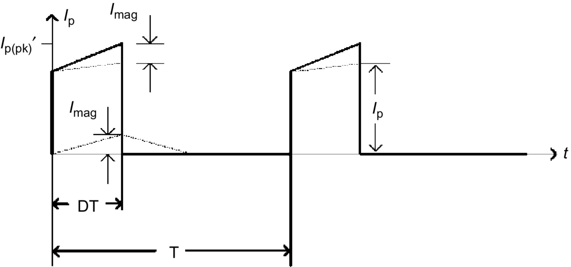

The magnetizing current in the primary has a magnitude of Imag and is given by

The total primary current Ip′ is then

The voltage developed across the secondary winding Vs is

Neglecting diode voltage drops and losses, the voltage across the output inductor is ![]() . The current in L1 increases linearly at the rate of
. The current in L1 increases linearly at the rate of
At the end of the on-time, the total primary current reaches a peak value equal to I′p(pk) and is given by

The output inductor current IL1 is

At the instant of turn-on, the amplitude of the secondary current has a value of Is(pk) and is given by

During the off-time, the current IL1 in the output inductor is equal to the current IDR3 in the rectifier diode DR3, and both decrease linearly at the rate of

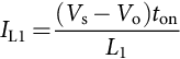
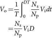
The output voltage Vo can be found from the time integral of the secondary winding voltage over a time equal to DT of the switch Q1. Thus, we have
The maximum collector current IC(max) at turn-on is equal to I′p(pk) and is given by

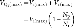
The maximum collector voltage ![]() at turnoff is equal to the maximum input voltage Vi(max) plus the maximum voltage Vr(max) across the tertiary winding and is given by
at turnoff is equal to the maximum input voltage Vi(max) plus the maximum voltage Vr(max) across the tertiary winding and is given by
The maximum duty cycle for the forward regulator operated in the continuous mode can be determined by equating the time integral of the input voltage when Q1 is on and the clamping voltage Vr when Q1 is off.

that leads to
Grouping the D terms in Eq. (20.58) and replacing Vr/Vi with Nr/Np, we have
Thus, the maximum duty cycle depends on the turn ratio between the demagnetizing winding and the primary one.
In designing forward regulators, the duty cycle must be kept below the maximum duty cycle Dmax to avoid saturating the transformer. It should also be noted that the transformer magnetizing current must be reset to zero at the end of each cycle. Failure to do so will drive the transformer into saturation, which can cause damage to the transistor. There are many ways of implementing the resetting function. In the circuit shown in Fig. 20.23A, a tertiary winding is added to the transformer so that the magnetizing current will return to the input source Vi when the transistor turns off. The primary current always starts at the same value under the steady-state condition.
Unlike flyback regulators, forward regulators require a minimum load at the output. Otherwise, excess output voltage will be produced. One commonly used method to avoid this situation is to attach a small load resistance at the output terminals. Of course, with such an arrangement, a certain amount of power will be lost in the resistor.
Because forward regulators do not store energy in their transformers, for the same output power level, the transformer can be made smaller than for the flyback type. The output current is reasonably constant owing to the action of the output inductor and the flywheel diode; as a result, the output filter capacitor can be made smaller, and its ripple current rating can be much lower than that required for the flybacks.
The forward regulator is widely used with output power below 200 W, though it can be easily constructed with a much higher output power. The limitation comes from the capability of the power transistor to handle the voltage and current stresses if the output power were to increase. In this case, a configuration with more than one transistor can be used to share the burden. Fig. 20.25 shows a double-ended forward regulator. Like the double-ended flyback counterpart, the circuit uses two transistors that are switched on and off simultaneously. The diodes are used to restrict the maximum collector voltage to Vi. Therefore, the transistors with low voltage rating can be used in the circuit.

20.5.3 Half-Bridge Regulators
The half-bridge regulator is another form of an isolated forward regulator. When the voltage on the power transistor in the single-ended forward regulator becomes too high, the half-bridge regulator is used to reduce the stress on the transistor. In a half-bridge regulator, the voltage stress imposed on the power transistors is subject to only the input voltage and is only half of that in a forward regulator. Thus, the output power of a half bridge is double to that of a forward regulator for the same semiconductor devices and magnetic core.
Fig. 20.26 shows the basic configuration of a half-bridge regulator and the associated steady-state waveforms. As seen in Fig. 20.26A, the half-bridge regulator can be viewed as two back-to-back forward regulators, fed by the same input voltage, each delivering power to the load at each alternate half cycle. The capacitors C1 and C2 are placed between the input and ground terminals. As such, the voltage across the primary winding is always half the input voltage. The power switches Q1 and Q2 are switched on and off alternatively to produce a square-wave ac at the input of the transformer. This square wave is either stepped down or up by the isolation transformer and then rectified by the diodes DR1 and DR2. Subsequently, the rectified voltage is filtered to produce the output voltage Vo.

Under steady-state condition, the operation of the regulator can be explained as follows. When Q1 is on and Q2 off, DR1 conducts and DR2 is reverse-biased. The primary voltage Vp is Vi/2. The primary current Ip starts to build up and stores energy in the primary winding. This energy is forward transferred to the secondary and onto the L1C filter and the load RL, through the rectifier diode DR1. During the time interval Δ, when both Q1 and Q2 are off, DR1 and DR2 are forced to conduct to carry the magnetizing current that resulted in the interval during which Q1 is turned on. The inductor current IL1 in this interval is equal to the sum of the currents in DR1 and DR2. This interval terminates at half of the switching period T, when Q2 is turned on. When Q2 is on and Q1 off, DR1 is reverse-biased and DR2 conducts. The primary voltage Vp is now ![]() . The circuit operates in a likewise manner as during the first half cycle.
. The circuit operates in a likewise manner as during the first half cycle.
With Q1 on, the voltage across the secondary winding is

Neglecting diode voltage drops and losses, the voltage across the output inductor is then given by

In this interval, the inductor current IL1 increases linearly at the rate of

At the end of Q1 on-time, IL1 reaches a value that is given by
During the interval Δ, IL1 is equal to the sum of the rectifier diode currents. Assuming the two secondary windings are identical, IL1 is given by
This current decreases linearly at the rate of

The next half cycle repeats with Q2 on and for the interval Δ.
The output voltage can be found from the time integral of the inductor voltage over a time equal to T. Thus, we have

Note that the multiplier of 2 appears in Eq. (20.66) because of the two alternate half cycles. Solving Eq. (20.66) for Vo, we have

The output power Po is given by
or
where Ip(avg) has the value of the primary current at the center of the rising or falling ramp. Assuming the reaction current Ip′ reflected from the secondary is much greater than the magnetizing current, then the maximum collector currents for Q1 and Q2 are given by

As mentioned, the maximum collector voltages for Q1 and Q2 at turnoff are given by
In designing half-bridge regulators, the maximum duty cycle can never be greater than 50%. When both the transistors are switched on simultaneously, the input voltage is short-circuited to ground. The series capacitors C1 and C2 provide a dc bias to balance the volt-second integrals of the two switching intervals. Hence, any mismatch in devices would not easily saturate the core. However, if such a situation arises, a small coupling capacitor can be inserted in series with the primary winding. A dc bias voltage proportional to the volt-second imbalance is developed across the coupling capacitor. This balances the volt-second integrals of the two switching intervals.
One problem in using half-bridge regulators is related to the design of the drivers for the power switches. Specifically, the emitter of Q1 is not at ground level, but is at a high ac level. The driver must therefore be referenced to this ac level. Typically, transformer-coupled drivers are used to drive both switches, thus solving the grounding problem and allowing the controller to be isolated from the drivers.
The half-bridge regulator is widely used for medium-power applications. Because of its core-balancing feature, the half bridge becomes the predominant choice for output power ranging from 200 to 400 W. Since the half bridge is more complex, for application below 200 W, the flyback or forward regulator is considered to be a better choice and more cost-effective. Above 400 W, the primary and switch currents of the half bridge become very high. Thus, it becomes unsuitable.
20.5.4 Full-Bridge Regulators
The full-bridge regulator is yet another form of isolated forward regulator. Its performance is improved over that of the half-bridge regulator because of the reduced peak collector current. The two series capacitors that appeared in half-bridge circuits are now replaced by another pair of transistors of the same type. In each switching interval, two of the switches are turned on and off simultaneously such that the full input voltage appears at the primary winding. The primary and the switch currents are only half that of the half bridge for the same power level. Thus, the maximum output power of this topology is twice that of the half bridge.
Fig. 20.27 shows the basic configuration of a full-bridge regulator and the associated steady-state waveforms. Four power switches are required in the circuit. The power switches Q1 and Q4 turn on and off simultaneously in one of the half cycles. Q2 and Q3 also turn on and off simultaneously in the other half cycle but with opposite phase as Q1 and Q4. This produces a square-wave ac with a value of ![]() at the primary winding of the transformer. Like the half bridge, this voltage is stepped down, rectified, and then filtered to produce a dc output voltage. The capacitor C1 is used to balance the volt-second integrals of the two switching intervals and prevent the transformer from being driven into saturation.
at the primary winding of the transformer. Like the half bridge, this voltage is stepped down, rectified, and then filtered to produce a dc output voltage. The capacitor C1 is used to balance the volt-second integrals of the two switching intervals and prevent the transformer from being driven into saturation.

Under steady-state conditions, the operation of the full bridge is similar to that of the half bridge. When Q1 and Q4 turn on, the voltage across the secondary winding is
Neglecting diode voltage drops and losses, the voltage across the output inductor is then given by

In this interval, the inductor current IL1 increases linearly at the rate of

At the end of Q1 and Q4 on-time, IL1 reaches a value that is given by

During the interval Δ, IL1 decreases linearly at the rate of
The next half cycle repeats with Q2 and Q3 on, and the circuit operates in a similar manner as in the first half cycle.
Again, as in the half bridge, the output voltage can be found from the time integral of the inductor voltage over a time equal to T. Thus, we have
Solving Eq. (20.77) for Vo, we have

The output power Po is given by

or

where Ip(avg) has the same definition as in the half-bridge case.
Comparing Eq. (20.80) with Eq. (20.69), we see that the output power of a full bridge is twice that of a half bridge with same input voltage and current. The maximum collector currents for Q1, Q2, Q3, and Q4 are given by
Comparing Eq. (20.81) with Eq. (20.70), for the same output power, the maximum collector current is only half that of the half bridge.
As mentioned, the maximum collector voltage for Q1 and Q2 at turnoff is given by
The design of the full bridge is similar to that of the half bridge. The only difference is the use of four power switches instead of two in the full bridge. Therefore, additional drivers are required by adding two more secondary windings in the pulse transformer of the driving circuit.
For high-power applications ranging from several hundred to thousand kilowatts, the full-bridge regulator is an inevitable choice. It has the most efficient use of magnetic core and semiconductor switches. The full bridge is complex and therefore expensive to build and is only justified for high-power applications, typically over 500 W.
20.5.5 Control Circuits and Pulse-Width Modulation
In previous subsections, we presented several popular voltage regulators that may be used in a switching mode power supply. This section discusses the control circuits that regulate the output voltage of a switching regulator by constantly adjusting the conduction period ton or duty cycle d of the power switch. Such adjustment is called pulse-width modulation (PWM).
The duty cycle is defined as the fraction of the period during which the switch is on, that is,
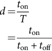
where T is the switching period, that is, ![]() . By adjusting either ton or toff or both, d can be modulated. Thus, PWM controlled regulators can operate at variable frequency and fixed frequency.
. By adjusting either ton or toff or both, d can be modulated. Thus, PWM controlled regulators can operate at variable frequency and fixed frequency.
Among all types of PWM controllers, the fixed-frequency controller is by far the most popular choice. There are two main reasons for their popularity. First, low-cost fixed-frequency PWM IC controllers have been developed by various solid-state device manufacturers, and most of these IC controllers have all the features that are needed to build a PWM switching power supply using a minimum number of components. Second, because of their fixed-frequency nature, fixed-frequency controllers do not have the problem of unpredictable noise spectrum associated with variable frequency controllers. This makes EMI control much easier.
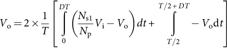
There are two types of fixed-frequency PWM controllers, namely, the voltage-mode controller and the current-mode controller. In its simplified form, a voltage-mode controller consists of four main functional components: an adjustable clock for setting the switching frequency, an output voltage error amplifier for detecting deviation of the output from the nominal value, a ramp generator for providing a sawtooth signal that is synchronized to the clock, and a comparator that compares the output error signal with the sawtooth signal. The output of the comparator is the signal that drives the controlled switch. Fig. 20.28 shows a simplified PWM voltage-mode controlled forward regulator operating at fixed frequency and its associated driving signal waveform. As shown, the duration of the on-time ton is determined by the time between the reset of the ramp generator and the intersection of the error voltage with the positive-going ramp signal.

The error voltage ve is given by
From Eq. (20.84), the small-signal term can be separated from the dc operating point by

The dc operating point is given by

Inspecting the waveform of the sawtooth and the error voltage shows that the duty cycle is related to the error voltage by

where Vp is the peak voltage of the sawtooth.
Hence, the small-signal duty cycle is related to the small-signal error voltage by

The operation of the fixed-frequency voltage-mode controller can be explained as follows. When the output is lower than the nominal dc value, a high error voltage is produced. This means that Δve is positive. Hence, Δd is positive. The duty cycle is increased to cause a subsequent increase in output voltage. The feedback dynamics (stability and transient response) is determined by the operational amplifier circuit that consists of Z1 and Z2. Some of the popular voltage-mode control ICs are SG1524/25/26/27, TL494/5, and MC34060/63.
The current-mode control makes use of the current information in a regulator to achieve output voltage regulation. In its simplest form, current-mode control consists of an inner loop that samples the inductance current value and turns the switches off as soon as the current reaches a certain value set by the outer voltage loop. In this way, the current-mode control achieves faster response than the voltage mode. There are two types of fixed-frequency PWM current-mode control, namely, the peak current-mode control and the average current-mode control.
In the peak current-mode control, no sawtooth generator is needed. In fact, the inductance current waveform is itself a sawtooth. The voltage analog of the current may be provided by a small resistance or by a current transformer. Also, in practice, the switch current is used since only the positive-going portion of the inductance current waveform is required. Fig. 20.29 shows a peak current-mode controlled flyback regulator.


In Fig. 20.29, the regulator operates at fixed frequency. Turn-on is synchronized with the clock pulse, and turnoff is determined by the instant at which the input current equals the error voltage Ve.
Because of its inherent peak current-limiting capability, the peak current-mode control can enhance reliability of power switches. The dynamic performance is improved because of the use of the additional current information. One main disadvantage of the peak current-mode control is that it is extremely susceptible to noise, since the current ramp is usually small compared with the reference signal. A second disadvantage is its inherent instability property at duty cycle exceeding 50%, which results in subharmonic oscillation. Typically, a compensating ramp is required at the comparator input to eliminate this instability. The third disadvantage is that it has a nonideal loop response because of the use of the peak, instead of the average current sensing.
Fig. 20.30 shows an average current-mode controlled flyback regulator. In the circuit, a PWM modulator (instead of a clocked SR latch in the peak current-mode control) is employed to compare the current error with an externally generated sawtooth signal to formulate the desired control signal. The main advantages of this method over the peak current control are that it has excellent noise immunity property, it is stable at duty cycle exceeding 50%, and it provides good tracking of average current. However, since there are three compensation networks (Z1, Z2, and Z3), the analysis and optimal design of these networks are nontrivial. This is a major obstacle for adopting the average current-mode control.

It should be noted that current-mode control is particularly effective for the flyback and boost-type regulators that have an inherent right-half-plane zero. Current-mode control effectively reduces the system to first order by forcing the inductor current to be related to the output voltage, thus achieving faster response. In the case of the buck-type regulator, current-mode control presents no significant advantage because the current information can be derived from the output voltage, and hence, faster response can still be achieved with a proper feedback network. Some of the popular current-mode control ICs are UC3840/2, UC3825, MC34129, and MC34065.