Electronic Ballasts
Jose Marcos Alonso University of Oviedo, Oviedo, Spain
Abstract
Electronic ballasts, also called solid-state ballasts, are those power electronic converters used to supply discharge lamps. The modern age of electronic ballasts began with the introduction of power bipolar transistors with low storage time, allowing to supply fluorescent lamps at frequencies of several kilohertz and increasing lamp luminous efficacy by operating at these high frequencies. Later, electronic ballasts became very popular with the development of low-cost power MOSFETs, with unique features that make them very attractive to implement solid-state ballasts. The main benefits of electronic ballasts are the increase in the lamp and ballast overall efficiency, increase in lamp life, reduction of ballast size and weight, and improvement in lighting quality. This chapter attempts to give a general overview about the more important topics related to this type of power converters.
Keywords
Discharge lamps; Lamp ballast; Electronic ballasts; Lamp modeling; Fluorescent lamps; Inverters; Resonant inverters; Power factor correction; THD; ZVS; Lumens
21.1 Introduction
Electronic ballasts, also called solid-state ballasts, are those power electronic converters used to supply discharge lamps. The modern age of electronic ballasts began with the introduction of power bipolar transistors with low storage time, allowing to supply fluorescent lamps at frequencies of several kilohertz and increasing lamp luminous efficacy by operating at these high frequencies. Later, electronic ballasts became very popular with the development of low-cost power MOSFETs, with unique features that make them very attractive to implement solid-state ballasts. The main benefits of electronic ballasts are the increase in the lamp and ballast overall efficiency, increase in lamp life, reduction of ballast size and weight, and improvement in lighting quality. This chapter attempts to give a general overview about the more important topics related to this type of power converters.
21.1.1 Basic Notions
Discharge lamps generate electromagnetic radiation by means of an electric current passing through a gas or metal vapor. This radiation is discrete, as opposed to the continuous radiation emitted by an incandescent filament. Fig. 21.1 shows the electromagnetic spectrum of an electric discharge, which consists of a number of separate spectral lines.
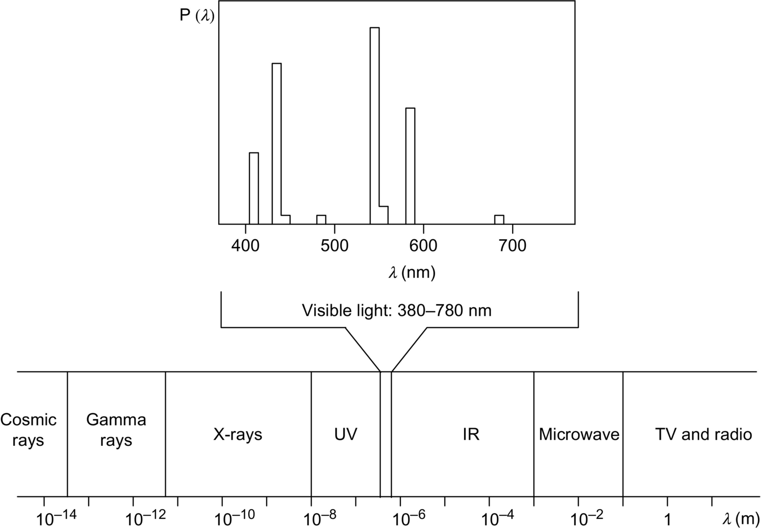
As can be seen in Fig. 21.1, only the electromagnetic radiation emitted within the visible region (380–780 nm) of the radiant energy spectrum is useful to provide lighting. The total power in watts emitted by an electric discharge can be obtained by integrating the spectral energy distribution. However, this is not a suitable parameter to measure the amount of light emitted by a discharge lamp.
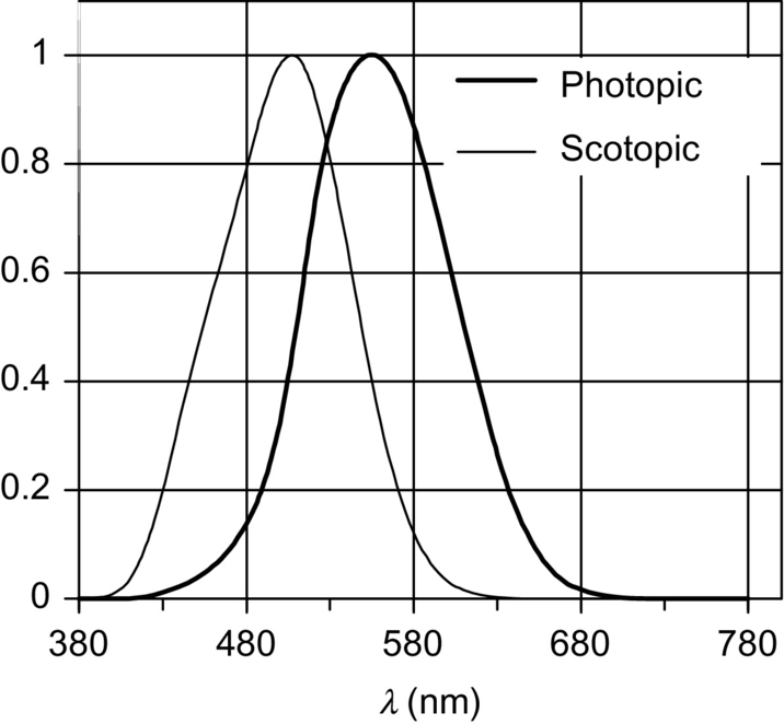
The human eye presents different responses to the different types of electromagnetic waves within the visible range. As illustrated in Fig. 21.2, there exist two response curves. First, the photopic curve, also called V(λ), is the characteristic used to represent the human eye under normal illuminating level conditions or daylight vision. Second, the scotopic curve V′(λ) is the response of the human eye for situations with low illuminating levels, also known as nocturnal vision. The reason for this different behavior is physiological. The human eye consists of two types of photoreceptors: rods and cones. Rods are much more sensitive at low lighting levels than cones, but they are not sensitive to the different light colors. On the other hand, cones are responsible for normal color vision at higher lighting levels. Normally, only the photopic function is considered in lighting design and used to calibrate photometers [1,2].
Since the human eye responds in different ways to the different wavelengths or colors, the output power of a lamp, measured in watts, is no longer applicable to represent the amount of light generated. Thus, a new unit is used to incorporate the human eye response, which is called lumen. The total light output of a lamp is then measured in lumens, and it is known as luminous flux of the lamp, which is obtained by integrating the radiant power as follows:
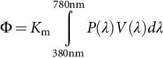
where Km represents the maximal spectral luminous efficacy, which is equal to 683 lm/W (at λ=555 nm) for photopic vision and 1700 lm/W (at λ=507 nm) for scotopic vision. The standard photopic and scotopic functions were defined by the International Commission on Illumination (CIE) in 1924 and 1951, respectively.
The measurement of the total luminous flux of the lamp is very useful to know whether the lamp is working properly. This can be measured by means of an integrating sphere and using the substitution method. The integrating sphere, also known as Ulbricht photometer, is internally coated with a perfectly diffusing material. Thus, the integral of the sphere is performed in Eq. (21.1), and the illuminance on the internal surface is proportional to the total luminous flux. A photometer with a V(λ) filter is placed so that the internal illuminance can be measured, and a baffle is located to avoid direct illumination of the photometer probe by the lamp. The measurement is made in two steps, one with the lamp under test in place and the other with a standard lamp of known total luminous flux. From the two measurements, the total luminous flux of the lamp under test is deduced by linear relationship. Fig. 21.3 illustrates an integrating sphere photometer.

An important parameter related to the supply of discharge lamps is the luminous efficacy. Luminous efficacy is defined as the rate of the lamp total luminous flux to the total electric power consumed by the lamp, usually expressed in lumens per watt. The luminous efficacy of a discharge lamp can be increased by proper designing of the electronic ballast, which finally results in energy saving.
21.1.2 Discharge Lamps
Basically, discharge lamps consist of a discharge tube inside, which the electric energy is transformed into electromagnetic radiation. The discharge tube is made of a transparent or translucent material with two sealed-in electrodes placed at both ends, as shown in Fig. 21.4. The discharge tube is filled with an inert gas and a metal vapor. The electrodes generate free electrons, which are accelerated by the electric field existing in the discharge. These accelerated electrons collide with the gas atoms, resulting in both elastic and inelastic collisions depending on the electron kinetic energy. The basic processes inside the discharge tube are illustrated in Fig. 21.4. They are as follows [3]:

1. Heat generation. When the kinetic energy of the electron is low, an elastic collision takes place, and only a small part of the electron energy is transferred to the gas atom. The result of this type of collisions is an increase in the gas temperature. In this case, the electric energy is consumed to produce heat dissipation. However, this is also an important process because the discharge has to be set in its optimum operating temperature.
2. Gas atom excitation. Some electrons can have a high kinetic energy so that the energy transferred in the collision is used to send an electron of the gas atom to a higher orbit. This state is unstable, and the electron tends to recover its original level, emitting the absorbed energy in the form of electromagnetic radiation. This radiation is used to directly generate visible light, or in other case, ultraviolet radiation is first generated and then transformed into visible radiation by means of a phosphor coating existing in the inside wall of the discharge tube.
3. Gas atom ionization. In some cases, electrons have gained such high kinetic energy that during the collision with the gas atom, an electron belonging to the gas atom is freed, resulting in a positively charged ion and a free electron. This freed electron can play the same roles as those generated by the electrodes. This process is especially important during both discharge ignition and normal running because ionized atoms and electrons are necessary to maintain the electric current through the lamp.
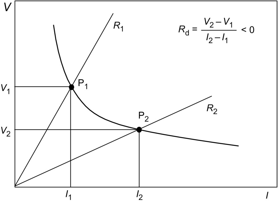
The number of free electrons in the discharge can increase rapidly due to continuing ionization, producing an unlimited current and finally a short circuit. This is illustrated in Fig. 21.5, which shows how the voltage-current characteristics of a gas discharge exhibit a negative differential resistance. Therefore, in order to limit the discharge current, the use of an auxiliary supply circuit is mandatory. This circuit is called ballast.
Focusing on discharge lamps, the complete stabilization process consists of two main phases:
1. Breakdown phase. Most of the gases are very good insulators, and an electric discharge is only possible if a sufficient concentration of charged particles is present. Normally, a high voltage is used to provide electricity carriers and to initiate the discharge. The minimum voltage applied to initiate the discharge is called starting voltage. The starting voltage mainly depends on the type of gas, gas pressure, and distance between electrodes. Fig. 21.6A represents the starting voltage as a function of the gas pressure multiplied by electrode distance, for different gases. These functions are known as Paschen curves.
Usually, auxiliary inert gases are used to decrease the starting voltage. Particularly, there exist some special inert gas mixtures presenting a very low starting voltage, which are called Penning mixtures. These Penning mixtures are very often used as initial starting gas. Fig. 21.6A shows a typical Penning mixture constituted by neon with 0.1% of argon.
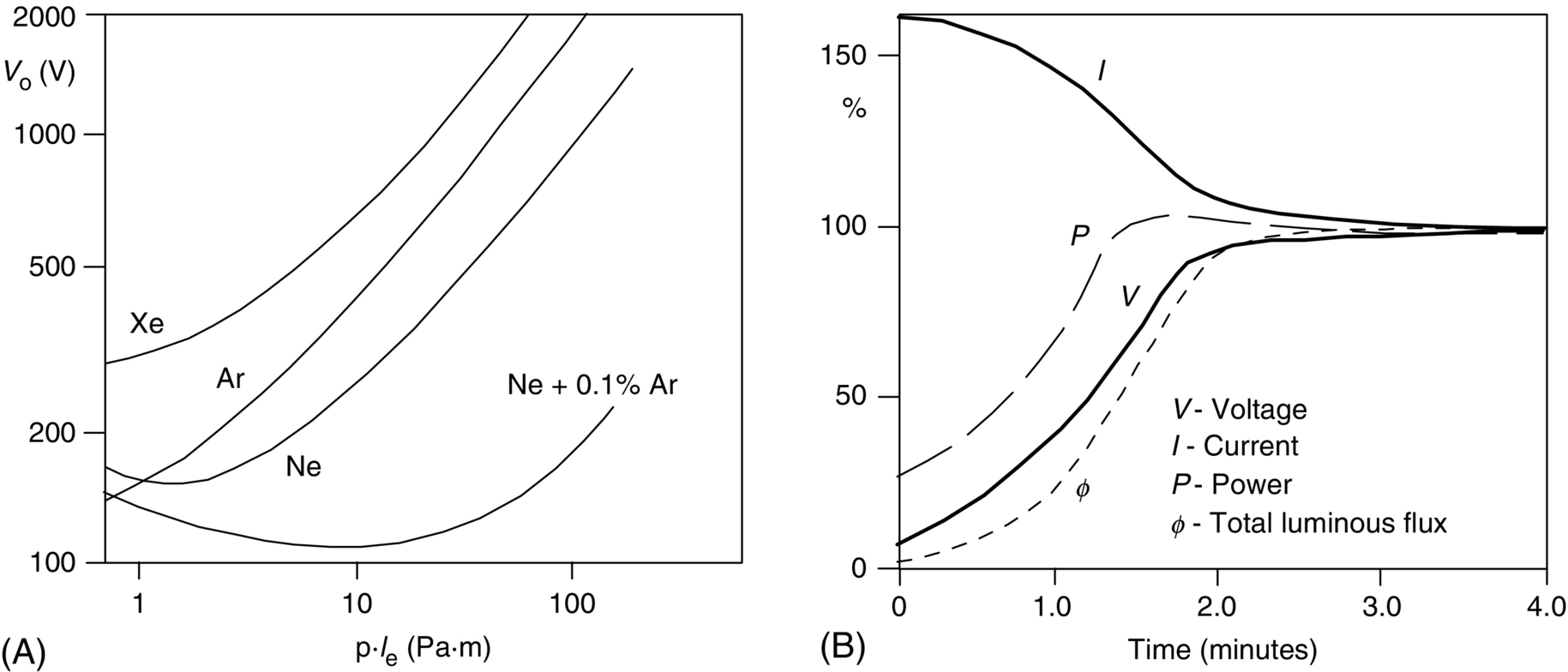
2. Warm-up phase. Once the lamp is ignited, the collisions between free electrons and atoms generate heat, and discharge temperature increases until reaching the normal operation conditions. During this phase, the heat is used to evaporate the metal atoms existing in the discharge tube, and the emitted electromagnetic radiation has the characteristics of a metal vapor discharge instead of an inert gas discharge. From the electric point of view, the discharge warm-up phase shows initially low discharge voltage and high discharge current. As long as more and more metal atoms are evaporated, the discharge voltage increases, and the discharge current decreases. Finally, an equilibrium is reached at steady-state operation with the normal values of voltage and current. The time constant of the warm-up phase strongly depends on the lamp type. It varies from seconds for fluorescent lamps to minutes for high-intensity discharge lamps. Fig. 21.6B illustrates some discharge waveforms during the warm-up phase.
The basic elements used in lamps to generate radiation in the visible part of the spectrum are sodium and mercury. The former generates radiation directly within the visible part of the spectrum; the latter generates radiation mainly in the ultraviolet region, but this radiation can be easily transformed to visible radiation by means of a phosphor coating on the internal wall of the discharge tube. Besides the element used, a very important parameter related to the efficiency and richness of the emitted radiation is the discharge pressure. For the sodium and mercury elements, there exist two pressure values around which the luminous efficacy of the discharge is higher. The first is obtained at quite low pressures, about 1 Pa, and the second at higher pressures around 105 Pa (1 at). This is the reason why there exist two main types of discharge lamps:
1. Low-pressure discharge lamps. This type of lamps operates with pressures around 1 Pa, and they feature low current density inside the discharge and low power/unit of discharge length. Therefore, these lamps present normally a quite large discharge volume with low power rating. Most representative examples are low-pressure mercury lamps, also known as fluorescent lamps and low-pressure sodium lamps.
2. High-pressure discharge lamps. The operating pressure in this type of lamps is around 105 Pa and higher, in order to achieve a considerable increase in the luminous efficacy of the discharge. These lamps present a high current density in the discharge and a high power/discharge length ratio, thus showing much smaller discharge tubes. Examples of these lamps are high-pressure sodium lamps, high-pressure mercury lamps, and metal halide lamps.
Finally, to characterize the light produced by a discharge lamp, it is necessary to know two important concepts: the correlated color temperature (CCT) and the color rendering index (CRI).
The CCT is defined as the temperature of the blackbody radiator whose perceived color most closely resembles that of the discharge lamp. The color of an incandescent body changes from deep red to orange, yellow, and finally white as its temperature rises. Thus, a cool-white fluorescent lamp has a CCT around 3500 K, and it is perceived as a white source of light, whereas a high-pressure sodium lamp presents a CCT of about 2000 K, and it appears as yellow.
The CRI of a light source is the effect that the source has on the color appearance of the objects under it, when compared with their appearance under a reference source of equal CCT. The measurement gives a value lower than 100, and the higher the CRI, the better the color rendition. For example, daylight and incandescent lamps have a CRI equal to 100.
To conclude this introduction on the discharge lamps, some comments regarding the most important types of discharge lamps will be given. Table 21.1 provides some additional data on the different discharge lamps for comparison.
Table 21.1
Comparison of different discharge lamps
| Lamp | Wattage (W) | Luminous efficacy (lm/W−1) | Life (h) | CCT (K) | CRI |
| Fluorescent | 4–100 | 62 | 20,000 | 4200 | 62 |
| Compact fluorescent | 7–30 | 60–80 | 10,000 | 2700–5000 | 82 |
| Low-pressure sodium | 50–150 | 110–180 | 15,000 | 1800 | <0 |
| Mercury vapor | 50–1000 | 40–70 | 24,000 | 4000–6000 | 15–50 |
| Metal halide | 40–15,000 | 80–125 | 10,000 | 4000 | 65 |
| HPS | 35–1000 | 65–140 | 24,000 | 2000 | 22 |
| HPS (amalgam) | 35–1000 | 45–85 | 10,000 | 2200 | 65 |

1. Fluorescent lamps. These lamps belong to the category of low-pressure mercury vapor discharge lamps. The discharge generates two main lines at 185 and 253.7 nm and other weak lines in the visible range of the spectrum. A fluorescent powder on the inside wall of the discharge tube converts the ultraviolet radiation into visible radiation, resulting in a broadband spectral distribution and good color rendition. In these lamps, the optimum mercury vapor pressure (which gives the maximum luminous efficacy) is 0.8 Pa. For the tube diameters normally used, this pressure is reached at a wall temperature of about 40°C, not much higher than typical ambient temperature. The heat generated inside the discharge is sufficient to attain the required operating temperature without using an outer bulb. However, this structure causes a great variation of the lamp lumen output with the temperature, which is one important drawback of the fluorescent lamps. One solution to this problem is the addition of amalgams to stabilize the light output. This is specially used in compact fluorescent lamps.
2. Low-pressure sodium lamps. These lamps are the most efficient source of light. The reason is the almost monochromatic radiation that they generate, with two main lines at 589 and 589.6 nm, very close to the maximum human eye sensitivity. Therefore, color rendition of these lamps is very poor; however, contrasts are seen more clearly under this light. This is the reason for using these lamps in situations where the recognition of objects and contours is essential for safety, such as motorway bridges, tunnels, and intersections. The optimum pressure for the low-pressure sodium discharge is about 0.4 Pa, which is attained in normal discharge tubes at a temperature of 260°C. An outer bulb is normally used to reach and maintain this temperature.
3. High-pressure mercury vapor lamps. The increase in the pressure of the mercury vapor produces a radiation richer in spectral lines; some of them are in the visible part of the spectrum (405, 436, 546, and 577/579 nm). This leads to an increase in the luminous efficacy, reaching values of 40–60 lm/W at pressures 105–107 Pa (1–100 at). These lamps operate with unsaturated mercury vapor, which means that all the mercury in the discharge tube has evaporated and the number of mercury atoms/unit volume remains constant. Thus, the operation of this type of lamps is more independent of the temperature than most other discharge lamps. One drawback of these lamps is the lack of spectral lines in the long wavelengths (reds) of the spectrum, thus showing low CRI. An increase of the color rendition can be obtained by adding metal halide compounds into the discharge tube, in order to generate radiation all over the visible spectrum. These lamps are known as metal halide lamps.
4. High-pressure sodium lamps. This is a very popular source of light due to its high luminous efficacy and long life. The increase in the sodium vapor pressure produces a very widening spectrum, with good color rendition compared with the low-pressure sodium lamps. This also leads to a lower luminous efficacy, but it is still higher than the other high-intensity discharge lamps. Some of these lamps also incorporate mercury in the form of sodium amalgam to increase the field strength of the discharge, thus decreasing the discharge current. A lower lamp current and a higher lamp voltage allow to reduce the size and cost of the ballast. However, the addition of sodium amalgam strongly reduces the life of the lamp.
21.1.3 Electromagnetic Ballasts
Electromagnetic ballasts are commonly used to stabilize the lamp at the required operating point by limiting the discharge current. The operating point of the lamp is given by the intersection of both lamp and ballast characteristics, as shown in Fig. 21.7. The ballast line is the characteristic that shows the variation of the lamp power versus lamp voltage for a constant line voltage, and it can be measured during the warm-up phase of the lamp. The lamp line is the characteristic that gives the variation of the lamp power as a function of the lamp voltage for different line voltages, and it can be measured by varying the line voltage. Some lamps, such as high-pressure sodium lamps, exhibit a great variation of lamp voltage with changes in the lamp wattage. Because of this characteristic, trapezoids have been established that define maximum and minimum permissible lamp wattage versus lamp voltage for purposes of ballast design, as shown in Fig. 21.7.
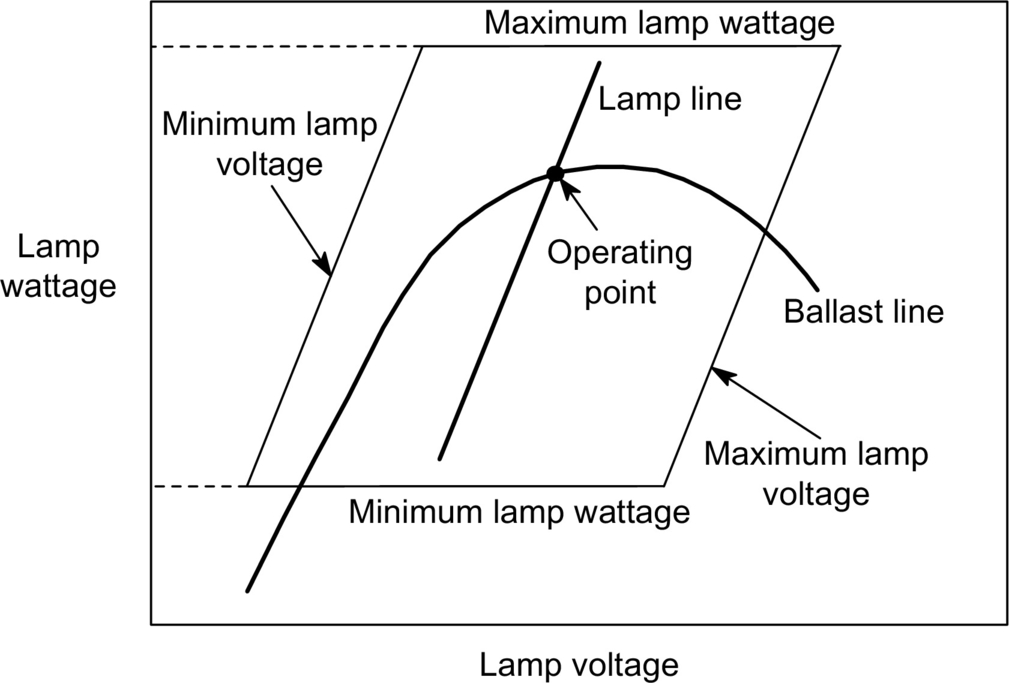
Fig. 21.8 shows a basic electromagnetic ballast used to supply low- and high-pressure lamps at line frequencies (50–60 Hz). Fig. 21.8A illustrates the typical circuit used to supply fluorescent lamps with preheating electrodes, which basically uses a series inductor to limit the current through the discharge. Initially, the glow switch is closed, and the short circuit current flows through the circuit, heating the electrodes. A fraction of a second later, the glow switch is opened, and the energy stored in the ballast inductor causes a voltage spike between the lamp electrodes (about 800 V), which finally produces the discharge breakdown. Once ignited, the lamp voltage is lower than the line voltage, and the glow switch remains open during the normal lamp operation. Typical glow switches are based on two bimetal strips inside a small tube filled with an inert gas. An external capacitor of about 10 nF is used to enhance the glow-switch operation and also to reduce radio interference during lamp starting. Finally, in this type of inductive ballasts, a capacitor placed across the line input is mandatory to achieve a reasonable value of the input power factor.

Starting voltages of high-pressure discharge lamps are normally higher than low-pressure discharge lamps and can range from 2500 V for a lamp at room temperature to 30–40 kV to reignite a hot lamp. Thus, the simple ignition system based on the glow switch is no longer applicable for these lamps. Fig. 21.8B and C shows two typical arrangements to supply high-intensity discharge lamps. A series inductor is also used to limit the lamp current at steady-state operation, but autotransformers are used to attain higher voltage spikes for lamp ignition. For higher line voltages and short distances between starter and lamp, the inductor ballast can be used as an ignition transformer as shown in Fig. 21.8B. In other cases, a separate igniting transformer is needed to provide higher voltage spikes and to avoid the effect of parasitic capacitance of connection cables (Fig. 21.8C).
The inductive ballast provides low-lamp-power regulation against line voltage variation, and therefore, it is only recommended in those installations with low voltage fluctuations. When a good lamp power regulation is necessary, the circuit shown in Fig. 21.8D is normally used. This circuit is commonly named as constant wattage autotransformer (CWA) and incorporates a capacitor in series with the lamp to limit the discharge current. Compared with the normal inductive ballast, the CWA also exhibits higher input power factor, lower line extinguishing voltage, and lower line starting currents.
The main advantage of electromagnetic ballasts is their simplicity, which in turn provides low cost and high reliability. However, since they operate at line frequencies, typically 50–60 Hz, they also feature high size and weight. Other important drawbacks of electromagnetic ballasts are as follows:
• Low efficiency especially for those ballasts featuring good lamp-power regulation against line voltage variation.
• Low reliability for ignition and reignition. If the voltage spike is not well located within the line period, the ignition of the lamp can fail.
• Difficult to control the lamp luminous flux (dimming).
• Lamp operating point changes due to lamp aging process, thus reducing lamp life.
• Low input power factor and high harmonic distortion. Large capacitors are needed across the line input to increase power factor.
• Overcurrent risk due to ballast saturation caused by rectifying effect of some discharge lamps, especially at the end of their life.
• Flickering and stroboscopic effect due to low frequency supply. The energy radiated by the lamp is a function of the instantaneous input power. Therefore, when supplied from an ac line, an instantaneous variation of the light output occurs, which is called flicker. For a line frequency of 60 Hz, the resulting light frequency is 120 Hz. This variation is too fast for the human eye, but when rapidly moving objects are viewed under these lamps, the objects seem to move slowly or even halted. This is called stroboscopic effect, and it can be very dangerous in industrial environments. A flicker index is defined with values from 0 to 1.0 [4]. The higher the flicker index the higher is the possibilities of noticeable stroboscopic effect.
• Unsuitable for dc applications (emergency lighting, automobile lighting, etc.).
21.2 High Frequency Supply of Discharge Lamps
21.2.1 General Block Diagram of Electronic Ballasts
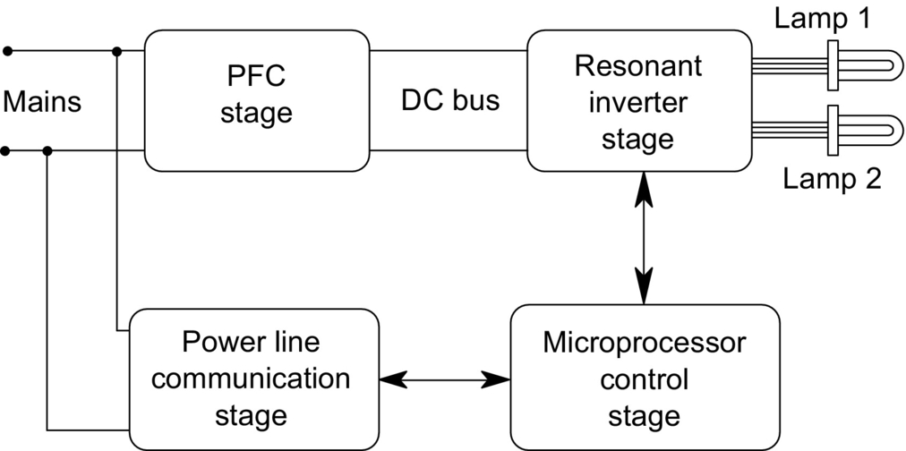
Fig. 21.9 shows the general block diagram of a typical electronic ballast. The main stages are the following:
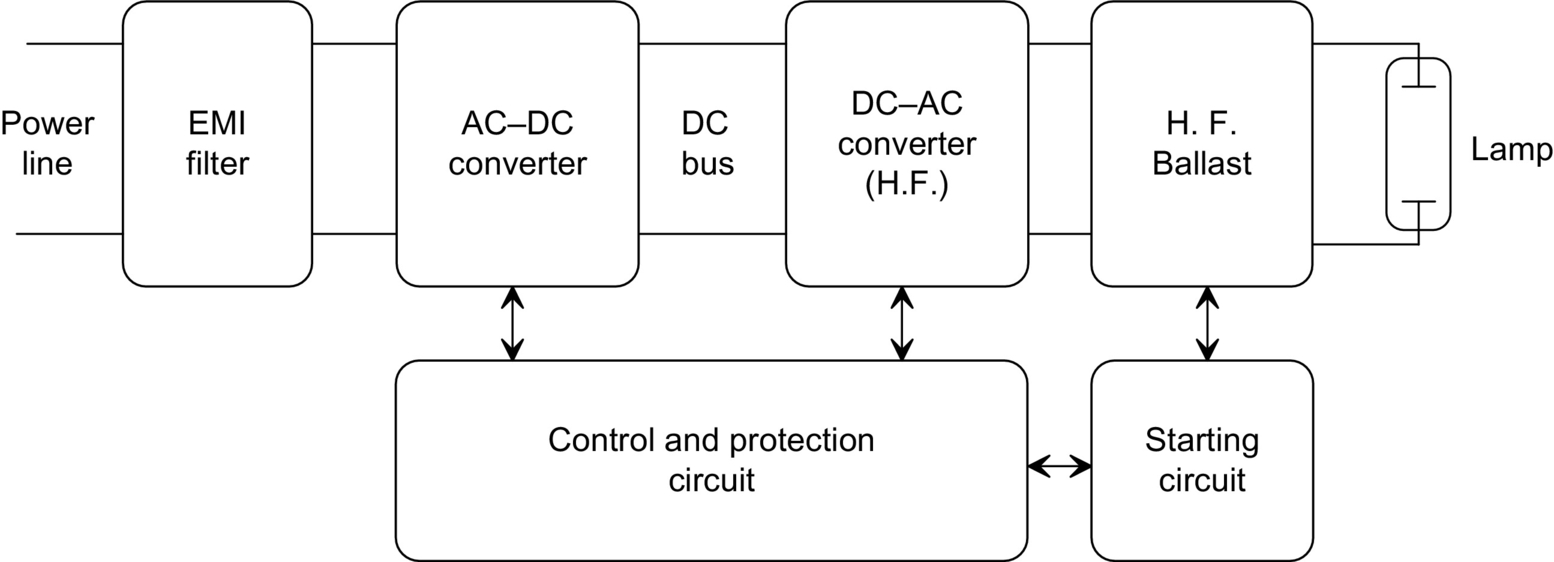
• EMI filter. This filter is mandatory for commercial electronic ballast. Usually, it consists of two coupled inductors and a capacitor. The input filter is used to attenuate the electromagnetic interference (EMI) generated by the high-frequency stages of the ballasts. It also protects the ballast against possible line transients.
• AC-DC converter. This stage is used to generate a dc voltage level from the ac line. Normally, a full-bridge diode rectifier followed by a filter capacitor is used. However, this simple rectifier provides low input power factor and poor voltage regulation. In order to obtain a higher power factor and a regulated bus voltage, active converters can be used as expounded later in this chapter.
• DC-AC inverter and high-frequency ballast. These stages are used to supply the lamp at high frequency. The inverter generates a high-frequency waveform, and the ballast is used to limit the current through the discharge. Both inductors and capacitors can be used to perform this function, with the advantage of low size and weight, because they operate at high frequencies.
• Starting circuit. In most electronic ballast, especially those for low-pressure discharge lamps, the high-frequency ballast is used to both ignite the lamp and limit the lamp current at steady state. Therefore, no extra starting circuit is necessary. However, when supplying high-pressure discharge lamps, the starting voltages are quite higher, and separate ignition circuits are needed, especially if hot reignition is pursued.
• Control and protection circuit. This stage includes the main oscillator, error amplifiers to regulate lamp current or power, output overvoltage protection, timers to control the ignition times, overcurrent protection, and lamp failure protection. It can vary from very simple circuits, those used in self-oscillating ballasts, to very complicated ones, which sometimes include a microprocessor-based control circuit.
There are several important topics when designing electronic ballasts:
• Operating frequency. The operating frequency should be high in order to take benefit of the lower size and weight of the reactive elements used to stabilize the discharge. Usually, the operating frequency should be higher than 20 kHz to avoid audible frequencies, which can produce annoying noises. On the other hand, a higher frequency produces higher switching losses, and the practical limit of the switching frequency is about 100 kHz when using MOSFET switches. It is also important to avoid frequencies in the range of 30–40 kHz because these frequencies are normally used in IR remote controls and could generate some kind of interference.
• Lamp current waveform. In order to attain the maximum lamp life, it is important to drive the lamp with symmetrical alternating currents, thus making use of both the lamp electrodes alternately. Also, an important parameter is the lamp current crest factor (CF), which is the ratio of the peak value to the rms value of the lamp current. In case of electronic ballasts, the ratio of the peak value of the low-frequency-modulated envelope to the rms value should be used. The higher the CF, the lower the lamp life. The ideal situation is to supply the lamp with a pure sinusoidal waveform. Usually, a CF lower than 1.7 is recommended to avoid early aging of the lamp [5].
• Lamp starting procedure. This is a very important issue when developing commercially available electronic ballasts. The reason is that the life of the lamp greatly depends on how well the lamp starting is performed, especially for hot-cathode fluorescent lamps. During the starting process, electrodes must be warmed up to the emission temperature, about 800°C, and no high voltage should be applied until their temperature is sufficiently high, thus avoiding sputtering damage. Once the electrodes reach the emission temperature, the starting voltage can be applied to ignite the lamp. For lamps with cold cathodes, the starting voltage must be applied rapidly to prevent harmful glow discharge and cathode sputtering. In any case, starting voltage must be limited to the minimum value to ignite the lamp, since higher voltages could provide undesirable starting conditions that would reduce the life of the lamp.
• Dimming. This is an important feature, which allows the ballast to control lamp power and thereby lighting output. Usually, the switching frequency is used in solid-state ballasts as a control parameter to provide dimming capability. Variations in frequency affect the high-frequency ballast impedance and allow to change the discharge current. For example, if an inductor is used as high-frequency ballast, a frequency increase yields an increase in the ballast impedance, thus decreasing lamp current. Dimming should be carried out smoothly, avoiding abrupt changes in lamp power when passing from one level to another. In an eventual power cutoff, the lamp should be restarted at maximum lighting level and then slowly reduced to the required output level.
• Acoustic resonance. The HID lamps exhibit an unstable operation when they are supplied at high frequency. At certain operating frequencies, the arc fluctuates and becomes unstable, which can be observed as a high flicker due to important changes in the lamp power and thus in the lighting output. This can be explained by the dependence of the damping of acoustic waves on the plasma composition and pressure. More information about this topic can be found in [6]. The avoidance of acoustic resonance is mandatory to implement commercial electronic ballasts. This can be performed by selecting the operating frequency in a range free of acoustic resonances, typically below 1 kHz and over 100 kHz. Other methods are frequency modulation, square-wave operation, and sine-wave superposed with the third harmonic frequency [7,8].
21.2.2 Classification of Electronic Ballast Topologies
Typical topologies used to supply discharge lamps at high frequency can be classified into two main groups: nonresonant ballasts and resonant ballasts.
21.2.2.1 Nonresonant Ballasts
These topologies are usually obtained by removing the output diode of dc-to-dc converters, in order to supply alternating current to the lamp. Current mode control is normally employed to limit the discharge lamp current. The lamp is supplied with a square current waveform, which can exhibit a dc level in some cases. A small capacitor is used to initially ignite the lamp, but its effect at steady-state operation can be neglected.
Examples of nonresonant electronic ballasts are shown in Fig. 21.10. Fig. 21.10A and b illustrates a boost-based and a flyback-based ballast, respectively. Other topologies, which can supply symmetrical alternating current through the lamp, are shown in Fig. 21.10C (symmetrical boost) and Fig. 21.10D (push-pull).
These topologies present several drawbacks such as high-voltage spikes across the switch, which necessitates the use of high-voltage transistors, and high switching losses due to hard switching, which gives low efficiency especially for high powers. Besides, since the ideal situation is the lamp being supplied with a sine wave, these circuits produce an early aging of the lamp. To conclude, typical applications of these topologies are portable and emergency equipments, in which lamp power is low and the number of ignitions during its life is not very high. Some applications of these circuits can be found in [9–12].
21.2.2.2 Resonant Ballasts
These ballasts use a resonant tank circuit to supply the lamp. The resonant tank filters the high-order harmonics, thus obtaining a sine current waveform through the lamp. Resonant ballasts can be classified into two categories:
Current-Fed resonant ballasts
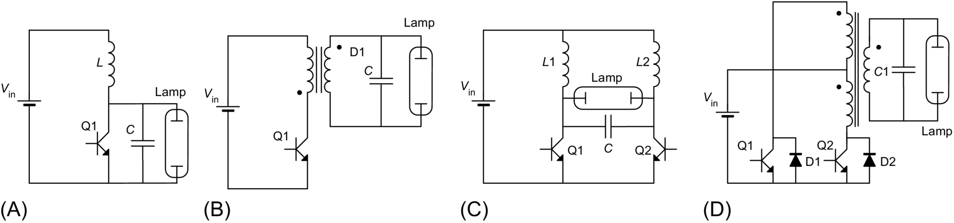
These ballasts are supplied with a dc current source, usually obtained by means of a choke inductor in series with the input dc voltage source. The dc current is transformed into an alternating square current waveform by switching power transistors. Typical topologies of this type of ballasts are shown in Fig. 21.11.
The topology shown in Fig. 21.11A corresponds to a class E inverter. Inductor Le is used to obtain a dc input current with low current ripple. This current supplies the resonant tank through the power switch formed by Q1-D1. The resonant tank used in this topology can vary from one ballast to another; the circuit shown in Fig. 21.11A is the one, which is normally used. The main advantage of this topology is that zero voltage switching (ZVS) can be attained in the power switch, thus reducing the switching losses and making the operation at very high frequencies, which can reach several megahertz. This allows to drastically reduce the size and weight of the ballast. However, the adjustment of the circuit parameters to obtain the optimum operation results is quite difficult, especially for mass production. Another important drawback is the high voltage stress across the switch, which can reach values of three times the dc input voltage. For these reasons, the main applications of this circuit are battery-supplied ballasts with low input voltage and low lamp power, as those used in emergency lighting and portable equipment. Typical power range of this ballast varies from 5 to 30 W. Applications of this circuit can be found in [13,14].
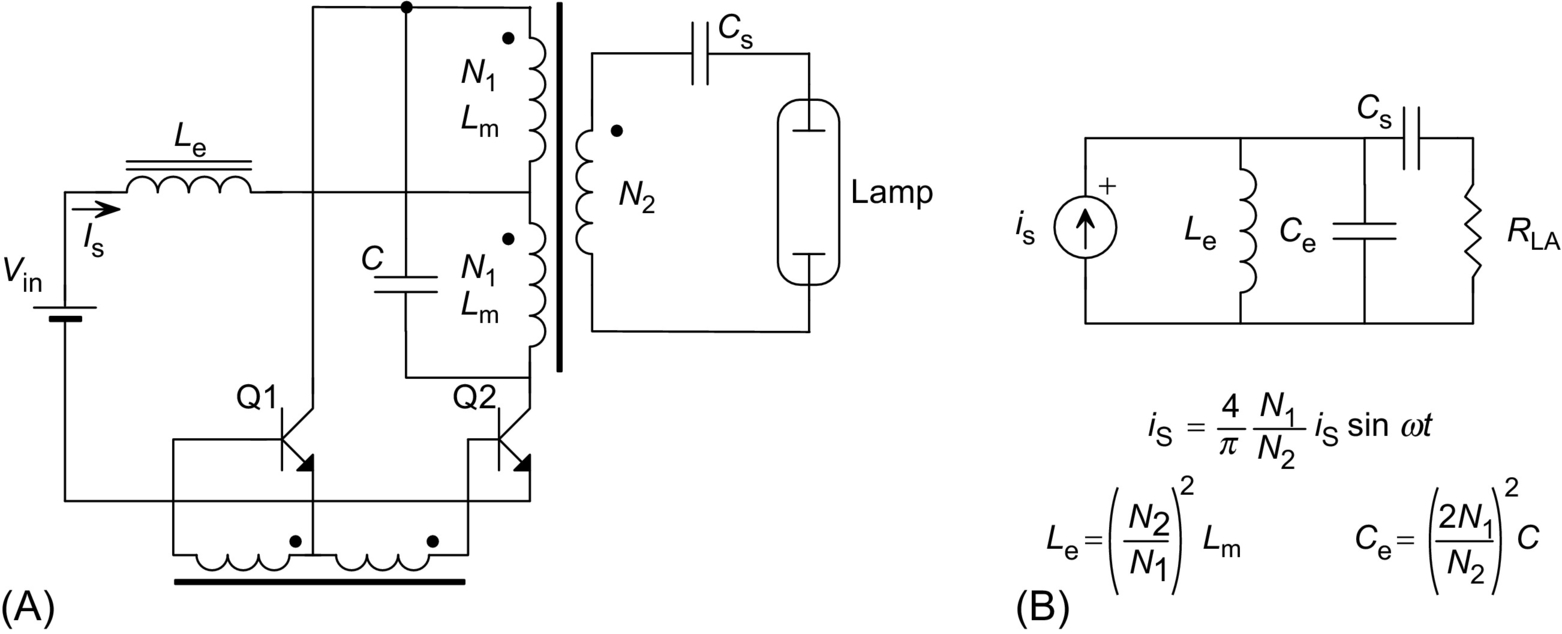
Another typical topology in this group is the current-fed push-pull inverter shown in Fig. 21.11B. In this circuit, a dc input current is obtained by means of choke inductor Le. Transistors are operated with a 50% duty cycle, thus providing a current square wave, which supplies the current-fed parallel resonant circuit formed by the mutual inductance of the transformer and capacitor C. This circuit has the advantage of being relatively easy to implement in a self-oscillating configuration, avoiding the use of extra control circuits and thereby reducing the cost. Also, ZVS can be obtained in the power switches. However, the switches also present a high voltage stress, about three times the dc input voltage, which makes this topology unsuitable for power line applications. This circuit is also normally used in battery-operated applications in a self-oscillating arrangement. The typical power range is 4–100 W. Applications based on this circuit can be found in [15,16].
Finally, Fig. 21.11C shows a current-fed full-bridge resonant inverter, which can be used for higher power rating. Also, this circuit allows to control the output power at constant frequency by switching the devices of the same leg simultaneously, generating a quasi-square current wave through the resonant tank [17].
Voltage-fed resonant ballasts
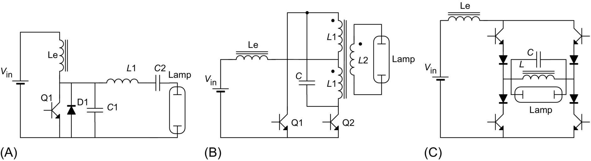
At present, electronic ballast manufacturers mostly use voltage-fed resonant ballasts, especially for applications supplied from the ac mains. The circuit is fed from a dc voltage source, normally obtained by line voltage rectifying. A square-wave voltage waveform is then obtained by switching the transistors with a 50% duty cycle and is used to feed a series resonant circuit. This resonant tank filters the high-order harmonics and supplies the lamp with a sine current waveform. One advantage of the voltage-fed series resonant circuit is that the starting voltage can be easily obtained without using extra ignition capacitors by operating close to resonant tank frequency. Fig. 21.12 shows electric diagrams of typical voltage-fed resonant ballasts.

The voltage-fed version of the push-pull inverter is illustrated in Fig. 21.12A. This inverter includes a transformer, which can be used to step up or down the input voltage in order to obtain an adequate rms value of the output square-wave voltage. This not only provides higher design flexibility but also increases the cost. One disadvantage is that the voltage across transistors is twice the input voltage, which can be quite high for line applications. Therefore, this inverter is normally used for low-voltage applications. Another important drawback of this voltage-fed inverter is that any asymmetry in the two primary windings (different number of turns) or in the switching times of power transistors would provide an undesirable dc level in the transformer magnetic flux, which in turn could saturate the core or decrease the efficiency due to the circulation of dc currents.
Fig. 21.12B and C illustrates two possible arrangements for the voltage-fed half-bridge resonant inverter. The former is normally referred as asymmetrical half bridge, and it uses one of the resonant tank capacitors (C1 in the figure) to block the dc voltage level of the square wave generated by the bridge. This means that capacitor C1 will exhibit a dc level equal to half the dc input voltage superimposed to its normal alternating voltage. A transformer can also be used in this inverter to step up or down the input voltage to the required level for each application. In this case, the use of the series capacitor C1 prevents any dc current from circulating through the primary winding, thus avoiding transformer saturation. This topology is widely used by ballast manufacturers to supply fluorescent lamps, especially in the self-oscillating version, which allows to drastically reduce the cost. When supplying hot-cathode fluorescent lamps, the parallel capacitor C2 is normally placed across two electrodes, as shown in Fig. 21.12B, in order to provide a preheating current for the electrodes and achieve soft ignition. Fig. 21.12C shows another version of the half-bridge topology, using two bulk capacitors to provide a floating voltage level equal to half the input voltage. In this case, capacitor C1 is no longer used to block a dc voltage, thus showing lower voltage stress.
Finally, for the high power range (>200 W), the full-bridge topology shown in Fig. 21.12D is normally used. The transistors of each half bridge are operated with a 50% duty cycle, and their switching signals are phase-shifted by 180 degrees. Thus, when switches Q1 and Q2 are activated, direct voltage Vin is applied to the resonant tank; when switches Q3 and Q4 are activated, the reverse voltage−Vin is obtained across the resonant circuit. One of the advantages of this circuit is that the switching signals of the two branches can be phase-shifted by angles between 0 and 180 degrees, thus controlling the rms voltage applied to the resonant tank ranging from 0 to Vin. This provides an additional parameter to control the output power at constant frequency, which is useful to implement dimming ballast.
21.3 Discharge Lamp Modeling
The low frequency of the mains is not an adequate power source for supplying discharge lamps. At these low frequencies, electrons and ionized atoms have enough time to recombine at each current reversal. For this reason, the discharge must be reignited twice within each line period. Fig. 21.13A illustrates the current and voltage waveforms and the I–V characteristics of a 150 W HPS lamp operated with an inductive ballast at 50 Hz. As can be seen, the reignition voltage spike is nearly 50% higher than the normal discharge voltage, which is constant during the rest of the half cycle.
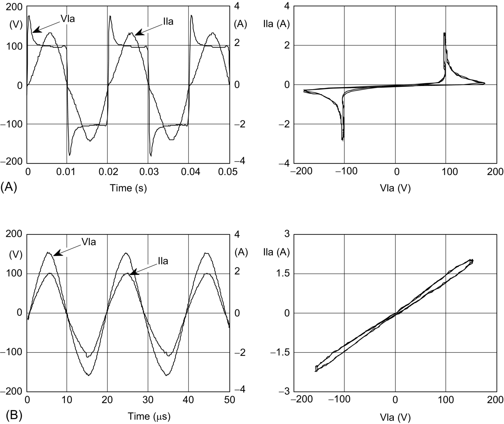
When lamps are operated at higher frequencies (above 5 kHz), electrons and ions do not have enough time to recombine. Therefore, charge carrier density is sufficiently high at each current reversal, and no extra power is needed to reignite the lamp. The result is an increase in the luminous flux compared with that at low frequencies, which is especially high for fluorescent lamps (10%–15%).
Fig. 21.13B shows the lamp waveforms and I–V characteristics for the same 150 W HPS lamp when supplied at 50 kHz. It also shows how the reignition voltage spikes disappear, and the lamp behavior is nearly resistive.
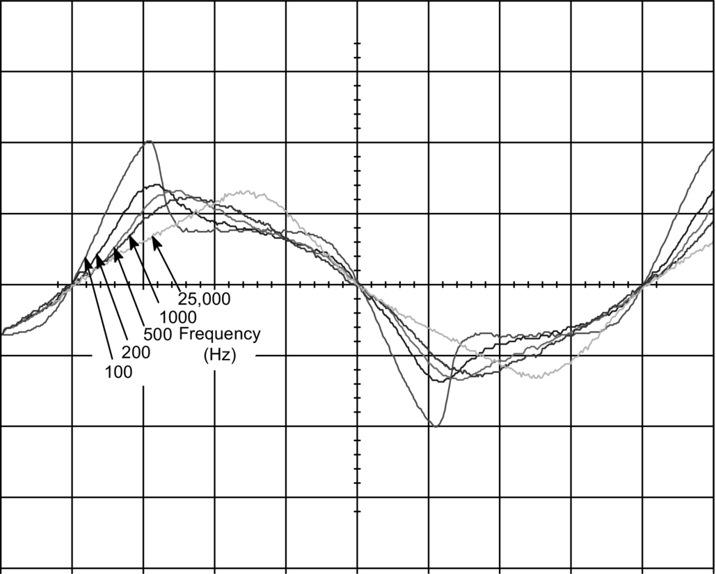
Fig. 21.14 illustrates how the voltage waveforms change in a fluorescent lamp when increasing the supply frequency. As can be seen, at a frequency of 1 kHz, the voltage is already nearly sinusoidal, and the lamp exhibits a resistive property.
Therefore, a resistor can be used to model the lamp at high frequencies for ballast design purposes. However, most lamp manufacturers provide only lamp data for operating at low frequencies, where the lamp acts as a square-wave voltage source. Table 21.2 shows the low-frequency electric data of different discharge lamps provided by the manufacturer and the measured values at high frequency for the same lamps. As can be seen, a power factor close to unity is obtained at high frequency.
Table 21.2
Electric data of different discharge lamps
| Lampa | Manufacturer at 50 Hz | Measured at H. F. | ||||||
| V (Vrms) | I (Arms) | P (W) | PF | V (Vrms) | I (Arms) | P (W) | PF | |
| Fluorescent (TLD-36 W) | 103 | 0.44 | 36 | 0.79 | 83.2 | 0.46 | 36 | 0.94 |
| Compact fluorescent (PLC-26 W) | 105 | 0.31 | 26 | 0.80 | 82 | 0.32 | 26 | 0.99 |
| Low-pressure sodium (SOX-55 W) | 109 | 0.59 | 55 | 0.86 | 75 | 0.76 | 56 | 0.98 |
| Mercury vapor (HPLN-125 W) | 125 | 1.15 | 125 | 0.87 | 132 | 0.92 | 120 | 0.99 |
| Metal halide (MHN-TD-150 W) | 90 | 1.80 | 150 | 0.93 | 92 | 1.63 | 146 | 0.97 |
| High-pressure sodium (SON-T-150 W) | 100 | 1.80 | 150 | 0.83 | 105 | 1.42 | 148 | 0.99 |
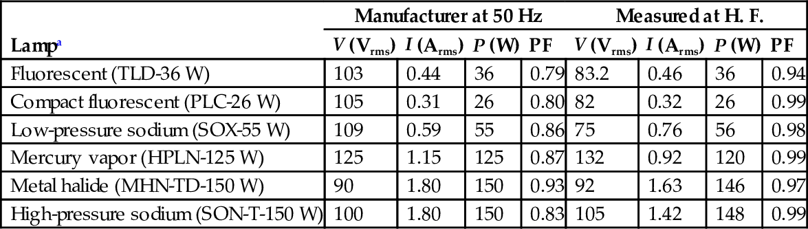
a Lamps aged for 100 h.
The equivalent lamp resistance at high frequencies can be easily estimated from the low-frequency data. Lamp power at any operating frequency can be expressed as follows:
where VLA and ILA are the rms values of lamp voltage and current and FPLA is the lamp power factor.
At line frequencies, the lamp power factor is low (typically 0.8), due to the high distortion in the lamp voltage waveform. However, at high frequencies, the lamp power factor reaches nearly 1.0. Then, lamp voltage and current at high frequency (VLA,hf and ILA,hf) can be estimated from the following equation:
where PLA is the nominal lamp power provided by the manufacturer.
As can be seen in Table 21.2, fluorescent lamps tend to maintain nearly the same rms current at low and high frequency, whereas high-pressure discharge lamps tend to maintain nearly the same rms voltage. Based on these assumptions, the equivalent lamp resistance at high frequency estimated from the low frequency values is shown in Table 21.3.
Table 21.3
Estimated electric data of discharge lamps at high frequency
| Lamp | VLA,hf | ILA,hf | RLA,hf |
| Fluorescent lamps | PLA/ILA,lf | ILA,lf | PLA/ILA,lf2 |
| High-pressure lamps | VLA,lf | PLA/VLA,lf | VLA,lf2/PLA |

Low-pressure sodium lamps maintain neither voltage nor current constant at high frequency, and they also exhibit an equivalent resistance quite dependent on the frequency. Therefore, their equivalent resistance can only be obtained by laboratory testing.
Note that the values given in Table 21.3 are only an approximation to the real value, which should be obtained by measurement at the laboratory. This can be used as the first starting point in the design of the electronic ballast, but final adjustments should be made at the laboratory.
Another important issue is that the lamp equivalent resistance is strongly dependent on power delivered to the lamp, which is especially important for designing electronic ballasts with dimming feature. The characteristic lamp resistance versus lamp power is different for each discharge lamp type and must be obtained by laboratory testing. One of the best possibilities to fit the lamp resistance versus power characteristic is the hyperbolic approximation. For example, Mader and Horn propose in [18] the following simple approximation:
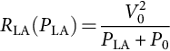
where RLA is the equivalent lamp resistance, PLA is the average lamp power, and V0 and P0 are two parameters that depend on each lamp. This characteristic has been plotted in Fig. 21.15 for a particular lamp with V0=100 V and P0=1 W.
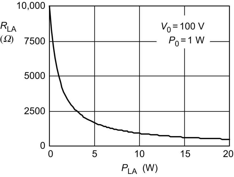
This model can be implemented very easily in circuit simulation programs, such as SPICE-based programs. Fig. 21.16 shows the electric circuit and the description used to model the characteristic of lamp in a SPICE-based simulation program. The voltage-controlled voltage source EL is used to model the resistive property of the lamp. The voltage source Vs is used to measure the lamp current, so that the instantaneous and average lamp current can be calculated; for this reason, its voltage value is equal to zero. GP is a voltage-controlled current source used to calculate the instantaneous lamp power, which is then filtered by RP and CP in order to obtain the averaged lamp power. Finally, the hyperbolic relationship between the lamp resistance and power is implemented by means of the voltage-controlled voltage source EK. The time constant τ=RP·CP is related to the ionization constant of the discharge.

Fig. 21.17 illustrates some simulation results at low frequency when the lamp is supplied from a sinusoidal voltage source and stabilized with an inductive ballast.
The Mader-Horn model can also be used at high frequencies, which makes the lamp resistive. The equivalent lamp resistance at high frequency will also exhibit a hyperbolic variation with the averaged lamp power and with a time constant given by τ. This model is then useful to simulate an electronic ballast with dimming feature.
Discharge lamp modeling has become an important subject, since its results are very useful to optimize the electronic ballast performance. Some improvements on the Mader-Horn model and other interesting models can be found in the literature [18–20].
21.4 Resonant Inverters for Electronic Ballasts
Most modern domestic and industrial electronic ballasts use resonant inverters to supply discharge lamps. They can be implemented in two basic ways: current-fed resonant inverters and voltage-fed resonant inverters.
21.4.1 Current-Fed Resonant Inverters
One of the most popular topologies belonging to this category is the current-fed push-pull resonant inverter, previously shown in Fig. 21.11. For this reason, this inverter will be studied here to illustrate the operation of the current-fed resonant ballasts.
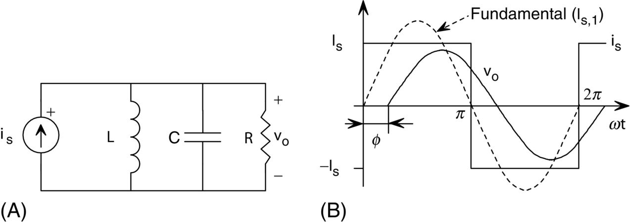
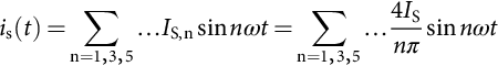
The current-fed push-pull inverter uses an input choke to obtain a dc input current with low current ripple. This current is alternatively conducted by the switches so that a parallel resonant tank can be supplied with a current square wave. Fig. 21.18 shows the equivalent circuit and the operating waveforms of a current-fed parallel resonant inverter.
The input current can be expressed as a Fourier series in the following way:
IS,n being the peak value of each current harmonic and IS the DC input current of the inverter. The output voltage for each current harmonic is obtained by multiplying the input current IS,n by the equivalent parallel impedance ZE,n, which is given below:

Usually, normalized values are employed in order to provide more general results. Then, the output voltage can be expressed as follows:
where ZB is the base impedance of the resonant tank, Q is the normalized load, Ω is the normalized frequency, and ω0 is the natural frequency of the resonant circuit, given by
From Eq. (21.7), the peak output voltage V0,n and phase angle φn can be obtained for each harmonic as follows:
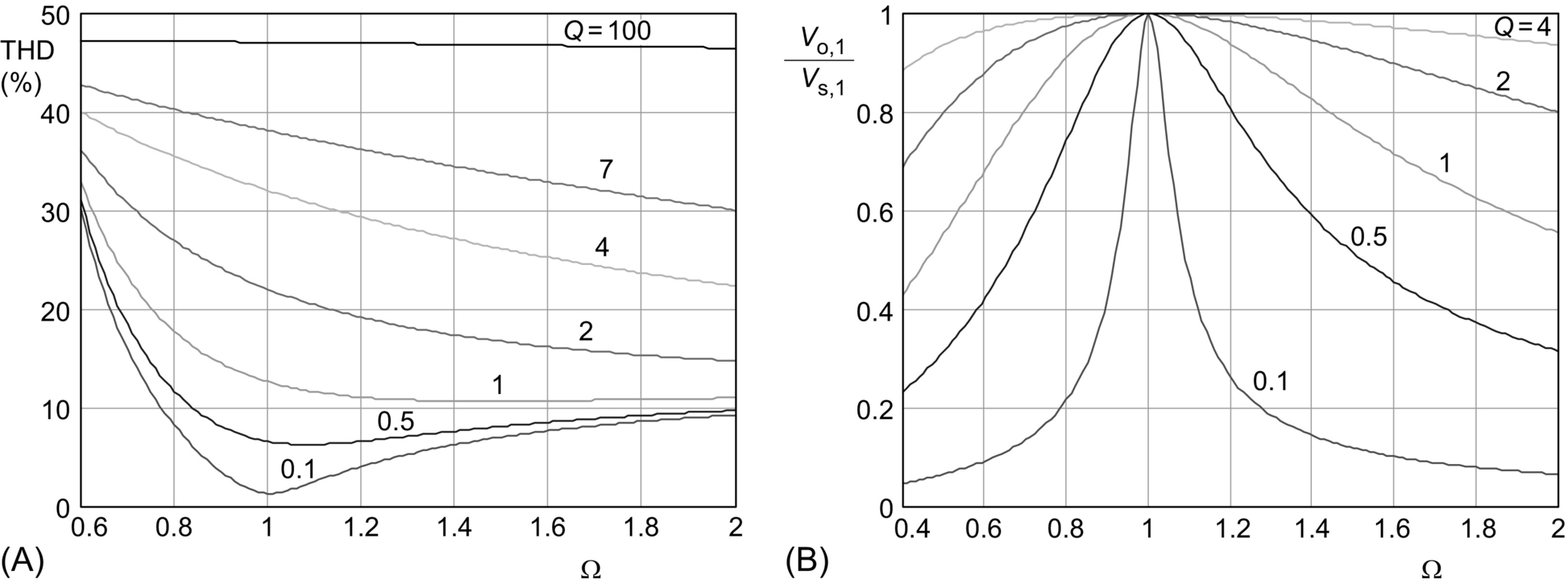
The total harmonic distortion (THD) of the output voltage can be calculated as follows:

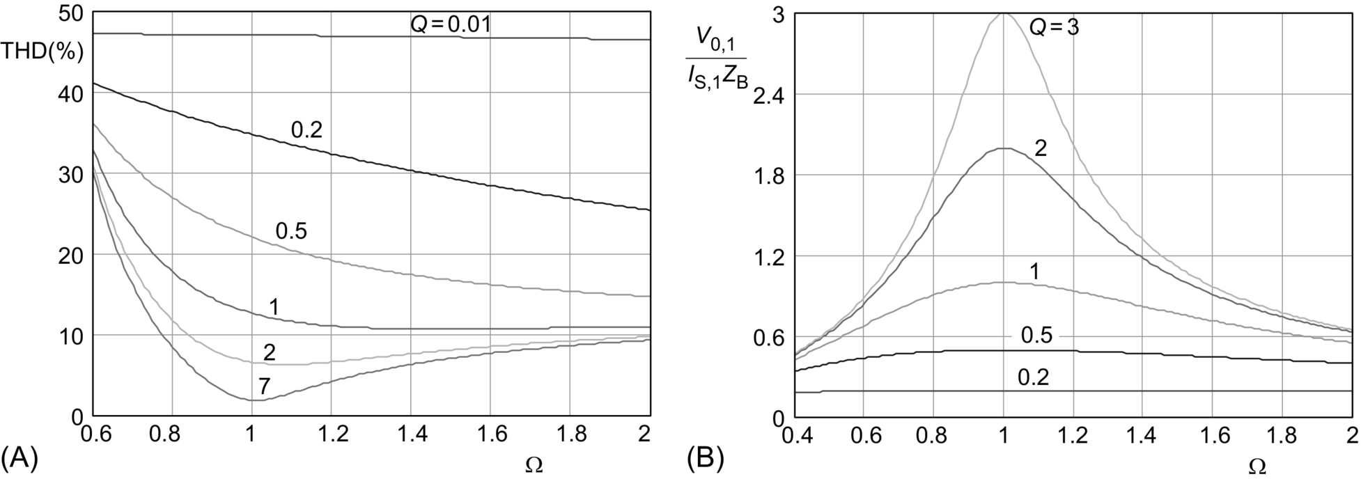
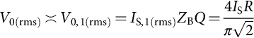
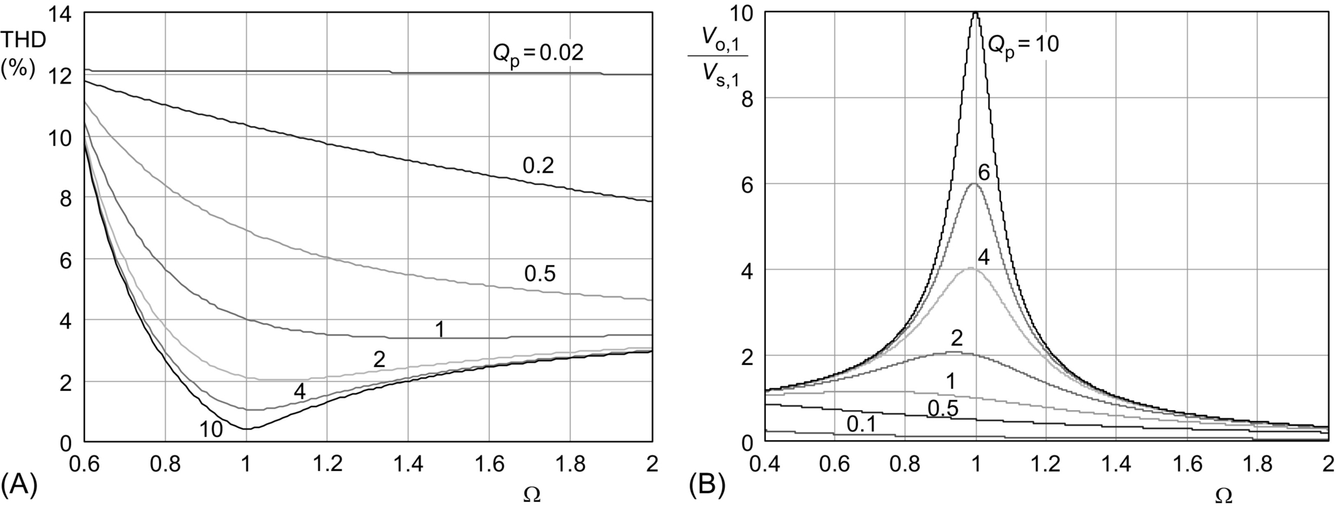
Based on these equations, the analysis and design of the current-fed resonant inverter can be performed. Normally, the circuit operates close to the natural frequency ω0, and the effect of the high frequency harmonics can be neglected. To probe this, Fig. 21.19A obtained by plotting Eq. (21.11) illustrates the THD of the output voltage as a function of the normalized load and frequency. As can be seen, for values of Q higher than 1 and for operation close to the natural frequency (Ω=1), the THD is low, which means that the output voltage is nearly a sinusoidal waveform. However, for low values of Q, the output voltage tends to be a square waveform, and the THD tends to the value of about 48%, corresponding to the THD of a square waveform. Fig. 21.19B illustrates the normalized output voltage for the fundamental component.
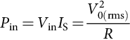
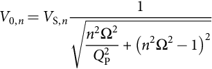
As stated previously, when used as lamp ballast, the current-fed parallel resonant inverter operates at the natural frequency of the resonant tank to both ignite the lamp and limit the current at normal running. Neglecting the effect of high-order harmonics, the rms output voltage is given by the fundamental component and can be obtained using Ω=1 in Eq. (21.9) as follows:
In a current-fed resonant inverter, the dc input current IS is supplied from a dc voltage source Vin with a series choke, as stated previously. Then, the dc input current can be obtained, assuming 100% efficiency, by equaling input and output power as follows:
And then,
Using Eq. (21.14) in Eq. (21.12) and solving for the output voltage,

As can be seen, when operating at the natural frequency, the rms output voltage is independent of the resonant tank load. The peak output voltage is equal to πVin/2. This value is directly related to the peak voltage stress in the switches. For a full-bridge topology, as shown in Fig. 21.11C, this value is equal to the switch voltage stress. However, for the current-fed push-pull inverter, the voltage stress is twice this value, which is πVin, due to the presence of the transformer. This gives a very high voltage stress for the switches in this topology, which is the reason why the current-fed push-pull is mainly used to implement low-input-voltage ballasts.
On the other hand, lamp starting voltage can vary from 5 to 10 times the lamp voltage in normal discharge mode. This makes the use of the current-fed parallel resonant inverter at constant frequency to both ignite the lamp and supply it at steady state difficult, since the output voltage is independent of the resonant tank load.
One solution to this problem is to ignite the lamp at the resonant tank natural frequency and then change the frequency to decrease the output voltage and output current to the normal running values of the lamp. This solution makes the use of extra circuitry to control the frequency necessary, normally in closed loop to avoid lamp instabilities, which increase the ballast cost.
Another solution, very often used in low-cost ballasts, is to design the parallel resonant tank to ignite the lamp and limit the lamp current in discharge mode by using an additional reactive element in series with the lamp. Normally, a capacitor is used to limit the lamp current in order to minimize the cost of the ballast. This solution is used in combination with the self-oscillating technique, which assures the operation at a constant frequency equal to the natural frequency of the resonant tank. Fig. 21.20A illustrates this circuit. Normally, the effect of the series capacitor is neglected, and the resonant tank is assumed to act as a sinusoidal voltage source during both ignition and normal operation, as shown in Fig. 21.20B. The high lamp starting voltage is obtained by means of a step-up transformer, which is the reason why typically a push-pull topology is used. If Vin is the dc input voltage and Vig is the lamp ignition voltage, then the necessary transformer turn ratio is given by the following expression:

The rms lamp current in discharge mode can be approximated as follows:
where R is the equivalent resistance of the lamp. From Eq. (21.17), the necessary value of the series capacitor CS, used to limit the lamp current to the nominal value ILA, can be easily obtained.
Finally, Fig. 21.21A and B illustrates a typical ballast based on a current-fed resonant inverter and its equivalent circuit, respectively.
21.4.2 Voltage-Fed Resonant Inverters
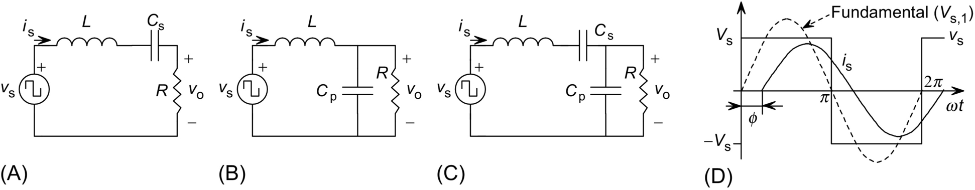
Some voltage-fed resonant inverters used to supply discharge lamps were previously shown in Fig. 21.12. Basically, they use two or more switches to generate a square voltage waveform. The different topologies are mainly given by the type of resonant tank used to filter this voltage waveform. There are three typical resonant tanks; their equivalent circuits are shown in Fig. 21.22. These circuits are the series-loaded resonant tank (Fig. 21.22A), the parallel-loaded resonant tank (Fig. 21.22B), and the series-parallel-loaded resonant tank (Fig. 21.22C). The typical operating waveforms are shown in Fig. 21.22D.
Similar to the current-fed resonant inverter, the input voltage can be expressed as a Fourier series in the following way:

VS,n being the peak value of each voltage harmonic and VS the dc input voltage of the inverter. The same methodology as that used to analyze the current-fed resonant inverter will be used here to study the property of the three basic voltage-fed resonant inverters.
21.4.2.1 Series-Loaded Resonant Circuit
The output voltage corresponding to the n-order harmonic is easily obtained as follows:
where QS and Ω are the normalized load and switching frequency given by the following expressions:
Fig. 21.23A shows the THD of the series-loaded circuit, and Fig. 21.23B shows the fundamental output voltage, which is normally considered for design purposes.
In this circuit, the input and output currents are equal and can be calculated by dividing the output voltage by the load impedance. This current is also circulating through the inverter switches and therefore represents an important parameter for the design. Another important parameter is the phase angle of the input current, which defines the type of commutations in the inverter switches. For the fundamental harmonic, the phase angle of the current circulating through the resonant tank can be calculated as follows:
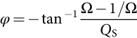
At the natural frequency (ω0), the input voltage and current will be in phase, which means that there is no reactive energy handled by the circuit and all the input energy is transferred to the load at steady-state operation. For frequencies higher than ω0, the current is lagged, and some reactive energy will be handled. In this case, the inverter switches will present ZVS [21]. For frequencies lower than ω0, the current is in advance, and also some reactive energy will be handled. In this case, the inverter switches will present zero current switching (ZCS).
As can be seen in Fig. 21.23A, the THD is lower for the lower values of the normalized load and for frequencies close to the natural frequency of the resonant tank. For the higher values of QS, the THD tends to the value corresponding to a square wave. The output voltage is always lower than the input voltage, and for frequencies around the natural frequency, the circuit acts as a voltage source, especially for the high values of QS. This means that the lamp cannot be ignited and supplied in discharge mode, maintaining a constant switching frequency. This property is similar to that encountered for the current-fed resonant inverter. The use of step-up transformers is mandatory to achieve lamp ignition, especially for the low input voltages. In order to maintain the operating frequency constant, a series element will be necessary to limit the lamp current at normal discharge operation. A capacitor can also be used as expounded in the previous section. In summary, this circuit is mainly used in high input voltage and low-current applications, and it is not very frequently used to implement electronic ballasts.
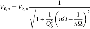
21.4.2.2 Parallel-Loaded Resonant Circuit
In this circuit, the output voltage corresponding to the n-order harmonic is given by the following expression:
where
The THD and fundamental output voltage are shown in Fig. 21.24. This circuit has characteristics very much useful to implement electronic ballasts than the series-loaded resonant circuit. First, the THD of the output voltage around the natural frequency is in general quite lower than that of the series circuit. For the lower values of QP, the THD tends to a value of 12%, which corresponds to the THD of a triangular wave. As a result, the lamp voltage and current waveforms will be very similar to a sine wave, which is an adequate waveform to supply the lamp. Second, the frequency response of the output voltage (Fig. 21.24B) makes it possible to both ignite the lamp and limit the lamp current at steady state, maintaining a constant operating frequency. During ignition, the lamp shows a very high impedance, thus giving a high value of QP. Under these conditions, the parallel circuit can generate a very high output voltage, provided that the operating frequency is close to the natural frequency. Once the lamp is ignited, the normalized load QP decreases, and the circuit can limit the lamp current without changing the operating frequency. In fact, the parallel circuit operating close to the natural frequency acts as a current source for the load, as will be shown later. This is adequate to supply discharge lamps because it assures a good discharge stability, avoiding the lamp being easily extinguished by transitory power fluctuations.
The maximum value of the voltage gain shown in Fig. 21.24 can be calculated to be equal to ![]() , and it appears at a frequency
, and it appears at a frequency ![]() . This means that a maximum is only present if QP is greater than
. This means that a maximum is only present if QP is greater than ![]() . For the higher values of QP, the maximum gain can be approximated to QP, and the frequency of maximum gain can be approximated to the natural frequency ω0.
. For the higher values of QP, the maximum gain can be approximated to QP, and the frequency of maximum gain can be approximated to the natural frequency ω0.
The input current of the parallel resonant circuit is another important parameter to calculate the current handled by the inverter switches. Since the operating frequency is normally around resonance, only the fundamental component is considered. The value of this fundamental current and its phase angle can be obtained as follows:
The condition for the input voltage being in phase with the input current can be obtained by equaling Eq. (21.25) to zero. This gives a value of the normalized frequency, which is ![]() . For a frequency greater than that value, the input current will lag the input voltage, and the inverter switches will present ZVS. For frequencies lower than that value, the current will be in advance, and zero current switching is obtained. The output voltage gain at that frequency is equal to QP.
. For a frequency greater than that value, the input current will lag the input voltage, and the inverter switches will present ZVS. For frequencies lower than that value, the current will be in advance, and zero current switching is obtained. The output voltage gain at that frequency is equal to QP.
Finally, it is very interesting to study the characteristic of this circuit for frequencies close to the natural frequency ω0 (Ω=1), since this is the normal region selected to operate for ballast applications. At this frequency, the output voltage gain is equal to QP, and then, the output current will be VS,1/ZB. This means that when operated at the natural frequency, the parallel circuit acts as a current source, whose value only depends on the input voltage. At the natural frequency, the input current is equal to ![]() , and the phase angle is equal to tan−1(−1/QP). The circuit is always inductive, with ZVS, and the phase angle decreases when QP increases, which means that less reactive energy is handled by the circuit.
, and the phase angle is equal to tan−1(−1/QP). The circuit is always inductive, with ZVS, and the phase angle decreases when QP increases, which means that less reactive energy is handled by the circuit.
21.4.2.3 Series-Parallel-Loaded Resonant Circuit
This circuit is also very widely used to implement electronic ballasts. The fundamental output voltage is given by the following expression:

where

and CE=CSCP/(CS+CP) is the series equivalent of the two capacitors present in this resonant circuit.
The fundamental input current and its phase angle are the following:
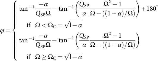
Fig. 21.25 shows the characteristics corresponding to the THD of the output voltage and the fundamental output voltage for α=0.5. As can be seen, the THD is also very low around the natural frequency, especially for the higher values of the normalized load QSP. Regarding the output voltage, this circuit acts as a parallel circuit around the natural frequency ω0, with a maximum gain voltage of about QSP/α. Around the natural frequency of the series circuit given by L and CS, ![]() , the circuit acts as a series-loaded circuit with a maximum voltage gain equal to unity.
, the circuit acts as a series-loaded circuit with a maximum voltage gain equal to unity.

The series-parallel circuit can also be used to both ignite and supply the lamp at constant frequency, since it also acts as a current source at the natural frequency. Besides, this circuit allows to limit the ignition voltage by means of the factor α, thus avoiding sputtering damage of lamp electrodes. Also, the series capacitor can be used to block any dc component of the inverter square output voltage, as that existing in the asymmetrical half bridge. In summary, the series-parallel circuit combines the best features of the series-loaded and the parallel-loaded; this is the reason why it is used widely to implement electronic ballasts.
When operated at frequency ω0, the output voltage gain is equal to QSP/α, and then, the circuit acts as a current source equal to VS,1/αZB, which is independent of the load. As stated previously, this current source behavior is adequate to supply discharge lamps because it allows the lamp current to be limited all the time. The input current phase angle at this frequency is equal to tan−1(−α/QSP), and the input current always lags the input voltage, thus showing ZVS operation.
Finally, the condition to have input current in phase with the input voltage can be obtained by equaling Eq. (21.27) to zero. This gives the following value:
Eq. (21.30) defines the borderline between the ZVS and the ZCS modes. The output voltage gain in this borderline can be obtained by using Eq. (21.30) in Eq. (21.26), and it is equal to ![]() .
.
21.4.3 Design Issues
The design methodology of a resonant inverter for discharge lamp supply can be very different depending on the lamp type and characteristics, inverter topology, design goals, etc. Some guidelines, especially focused for supplying fluorescent lamps with voltage-fed resonant inverters, are presented in this section to illustrate the basic design methodology.
A typical starting process for a hot-cathode fluorescent lamp is shown in Fig. 21.26. Initially, lamp electrodes are heated up to the emission temperature. During this phase, the inverter should assure a voltage applied to the lamp not high enough to produce sputtering damage in lamp electrodes, thus avoiding premature aging of the lamp. Once electrodes reach the emission temperature, the lamp can be ignited by applying the necessary starting voltage. Following this procedure, a soft starting is achieved, and a long lamp life is assured.
The best method to perform this soft starting is to control the inverter switching frequency, so that the lamp voltage and current are always under control. During the heating process, the operating frequency is adjusted to a value above the natural frequency of the resonant tank. In this way, the heating current can be adjusted to the necessary value, maintaining a lamp voltage quite lower than the starting voltage. Since normally MOSFET or bipolar transistors are used, the operation over the natural frequency is preferable because they provide ZVS, and the slow parasitic diodes existing in these transistors can be used. After a short period of time, the switching frequency is reduced until the starting voltage is obtained, and then, the lamp is ignited. Normally, the final operating point at steady-state operation is adjusted to be at a switching frequency equal to the natural frequency, so that a very stable operation for the lamp is assured.
Fig. 21.27A shows a fluorescent lamp supplied using a series-parallel-loaded resonant tank. The input data for the design are normally the fundamental input voltage VS, the switching frequency in normal discharge operation (running) fS, the lamp voltage and current at high frequency VLA and ILA, the electrode heating current IH, the maximum lamp voltage during heating process VH, and the lamp starting voltage VIG.
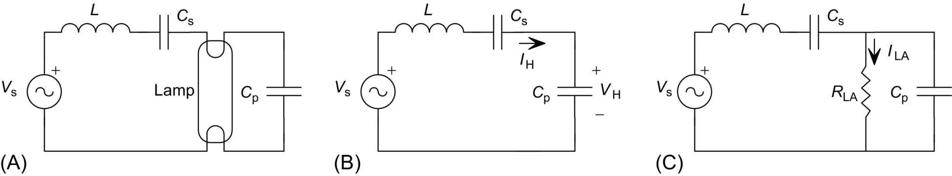
The equivalent circuit during the heating and ignition phase is shown in Fig. 21.27B. The current circulating in this circuit is the electrode heating current, which can be calculated by using QSP=∞ in Eq. (21.24):

where the electrode resistance has been neglected for simplicity. For a given heating current IH, the necessary switching frequency is obtained from Eq. (21.31) as follows:
Regarding the heating voltage, it can be calculated from Eq. (21.26) using QSP=∞, and the following value is obtained:

The frequency at which the starting voltage is achieved can also be obtained using QSP=∞ in Eq. (21.26), giving the following value:

Once the lamp is ignited, the new operation circuit is shown in Fig. 21.27C. Normally, the switching frequency is selected to be very close to the natural frequency, and the circuit characteristics can be obtained by using Ω=1. Thus, as stated previously, the circuit acts as a current source of the following value:

From this equation, the impedance ZB needed to provide a lamp current equal to ILA is easily obtained:

Using Eqs. (21.31)–(21.36), the design procedure can be performed as follows:
Step 1 Steady-state operation. Choose a value for the factor α; normally, a value of 0.8–0.9 will be adequate for most applications. From Eq. (21.36), calculate the value of ZB for the resonant tank. Since the natural frequency is equal to the switching frequency, the reactive elements of the resonant tank can be calculated as follows:
Step 2 Heating phase. From Eq. (21.32), calculate the switching frequency for a given heating current IH. Then, calculate the value of the heating voltage VH from Eq. (21.33).
Step 3 Check if the heating voltage is lower than the maximum value allowed to avoid electrode sputtering. If the voltage is too high, choose a lower value of α and repeat steps 1 and 2. Also, the maximum heating frequency can be limited to avoid excessive frequency variation. The lower the α, the lower is the frequency variation from heating to ignition, since the output voltage characteristics are narrower for the lower values of α.
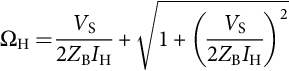
The described procedure to achieve lamp soft ignition requires the use of a voltage-controlled oscillator to control the switching frequency. This can increase the cost of the ballast. A similar soft ignition can be achieved using the resonant circuit shown in Fig. 21.28. This circuit is very often used in self-oscillating ballasts, where the switches are driven from the resonant current using a current transformer [22].
In the circuit shown in Fig. 21.28, the PTC is initially cold, and capacitor CP1 is practically short-circuited by the PTC. The resonant tank under these conditions is formed by L-CS-CP2, which can be designed to heat the lamp electrodes with a heating voltage low enough to avoid lamp cold ignition. Since the PTC is also heated by the circulating current, after a certain period of time, it reaches the threshold temperature and trips. At this moment, the new resonant tank is formed by L, CS, and the series equivalent of CP1 and CP2. This circuit can be designed to generate the necessary ignition voltage and to supply the lamp in normal discharge mode. Once the lamp is ignited, the PTC maintains its high impedance since the dominant parallel capacitor in this phase is CP1 (usually CP1≪CP2).
21.5 High-Power Factor Electronic Ballasts
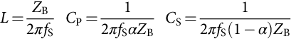
As commented in a previous section, when electronic ballasts are supplied from the ac line, an ac-dc stage is necessary to provide the dc input voltage of the resonant inverter (see Fig. 21.9). Since the introduction of harmonic regulations, as IEC 1000-3-2, the use of a full-bridge diode rectifier followed by a filter capacitor is no longer applicable for this stage due to the high harmonic content of the input current. Therefore, the use of an ac-dc stage showing a high input power factor (PF) and a low total harmonic distortion (THD) of the input current is mandatory. The inclusion of this stage can significantly increase the cost of the complete ballast, and therefore, the search for low-cost high-power-factor electronic ballasts is presently an important field of research.
Fig. 21.29A shows a first possibility to increase the input power factor of the ballast by removing the filter capacitor across the diode rectifier. However, since there are no low-frequency storage elements inside the resonant inverter, the output power instantaneously follows the input power, thus producing an annoying light flicker. Besides, the resulting lamp current crest factor is very high, which considerably decreases lamp life.
In order to avoid flicker and increase lamp current crest factor, continuous power must be delivered to the lamp. This can only be accomplished by using a PFC stage with a low-frequency storage element. This solution is shown in Fig. 21.29B, where capacitor C0 is used as energy storage element. The main drawback of this solution is that the input power is handled by the two stages, which reduces the efficiency of the complete electronic ballast.
21.5.1 Harmonic Limiting Standards
The standards IEC 1000-3-2 and EN 61000-3-2 [23] are the most popular regulations regarding the harmonic pollution produced by electronic equipment connected to the mains. These standards are a new version of the previous IEC 555-2 regulation, and they are applicable to the equipment with less than 16 A/phase and supplied from low voltage lines of 220/380 V, 230/400 V, and 240/415 V at 50 or 60 Hz. Limits for equipment supplied from voltages lower than 220 V have not yet been established.
This regulation divides the electric equipment in several classes from class A to class D. Class C is especially for lighting equipment, including dimming devices; the harmonic limits for this class are shown in Table 21.4. As shown in Table 21.4, this regulation establishes a maximum amplitude for each input harmonic as a percentage of the fundamental harmonic component. The harmonic content established in Table 21.4 is quite restrictive, which means that the input current wave must be quite similar to a pure sine wave. For example, for a typical input power factor equal to 0.9, the THD calculated from Table 21.1 is only 32%.
21.5.2 Passive Solutions
A first possibility to increase the ballast power factor and to decrease the harmonic content of the input current is the use of passive solutions. Fig. 21.30 shows two typical passive solutions, which can be used to improve the input power factor of electronic ballasts.
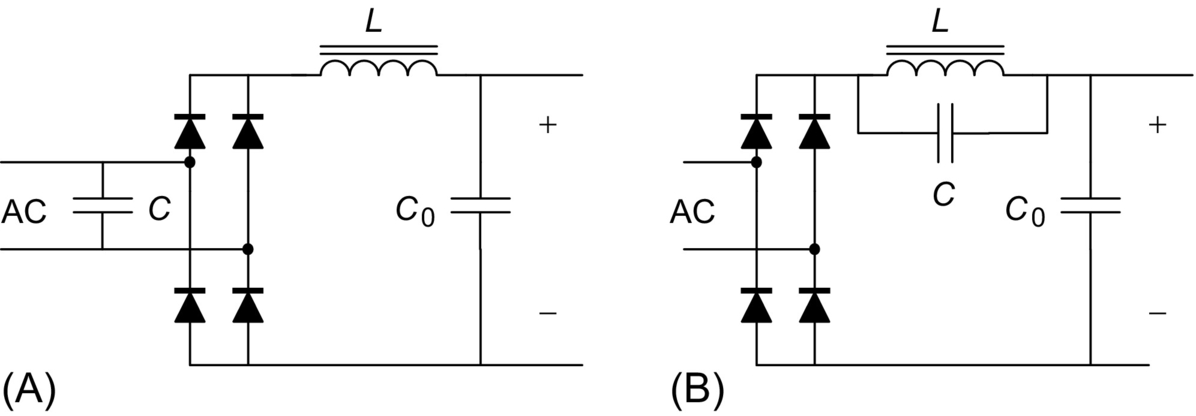
Fig. 21.30A shows the most common passive solution based on a filter inductor L. Using a large inductance L, a square input current can be obtained, with an input power factor of 0.9 and a THD of about 48%. However, a square input waveform does not satisfy the IEC 1000-3-2 requirements, and then, it is not a suitable solution. The addition of capacitor C across the ac terminals can increase the power factor up to 0.95, but still, the standard requirements are difficult to fulfill.
A simple variation of this circuit is shown in Fig. 21.30B, where a parallel circuit tuned to the third harmonic of the line frequency is used to improve the shape of the line current. The input power factor obtained with this circuit can be close to unity.
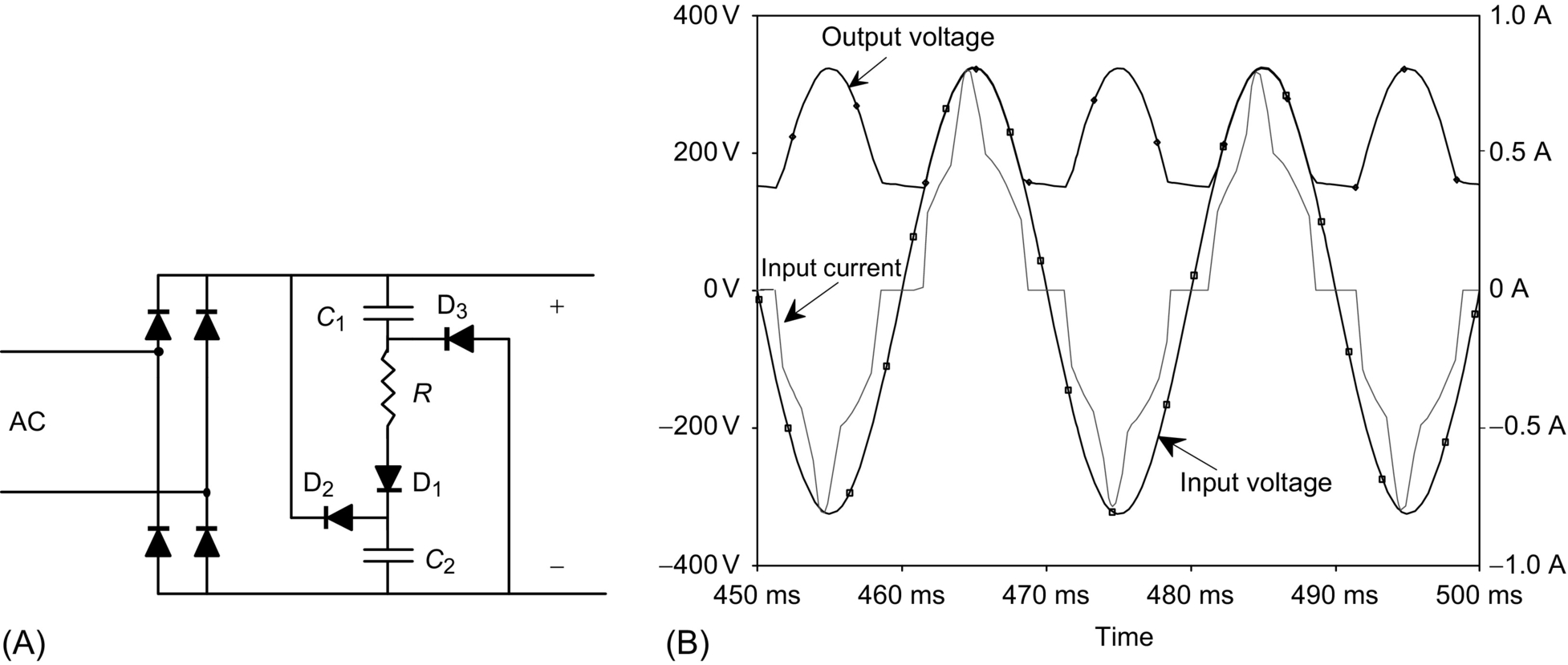
A third possible solution, known as valley-fill circuit, is shown in Fig. 21.31A. The typical filter capacitor following the diode rectifier is split into two different capacitors that are alternately charged using three extra diodes. The addition of a small series resistor improves the power factor by about two points, maintaining a low cost for the circuit. An inductor in place of the resistor can also be used to improve the power factor but with a higher cost penalty. Fig. 21.31B shows the output voltage and input current of the valley-fill circuit. The main disadvantage of this circuit is the high ripple of the output voltage, which produces lamp power and luminous flux fluctuation and high lamp current crest factor.
Passive solutions are reliable, rugged, and cheap. However, the size and weight of these solutions are high, and their design to fulfill the IEC 1000-3-2 requirements is usually difficult. Therefore, they are normally applied in the lower power range.
21.5.3 Active Solutions
Active circuits are the most popular solutions to implement high-power-factor electronic ballasts. They use controlled switches to correct the input power factor and in some cases to include galvanic isolation via high-frequency transformers. Active circuits normally used in electronic ballasts operate at a switching frequency well above the line frequency and over the audible range.
Some typical active circuits used in electronic ballasts are shown in Fig. 21.32. Buck-boost and flyback converters shown in Fig. 21.32A and B, respectively, can be operated in discontinuous conduction mode (DCM) with constant frequency and constant duty cycle in order to obtain an input power factor close to unity [24].
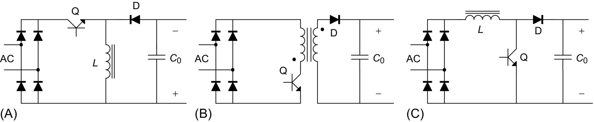
Fig. 21.32C shows the boost converter, which is one of the most popular active circuits used to correct the input power factor of electronic ballasts [25–27]. If the boost converter is operated in DCM, an input power factor close to unity is obtained, provided that the output voltage is about twice the peak input voltage [25]. The main disadvantage of DCM operation, when compared with the CCM mode, is the high distortion of the input current (due to the discontinuous high-frequency current) and the higher current and voltage stresses in the switches. Therefore, the DCM operation is only used for the lower power range.
For the medium power range, the operation of the boost converter at the DCM-CCM borderline is preferred. In this solution, the on time of the controlled switch is maintained constant within the whole line period, and the switching frequency is adjusted to allow the input current to reach zero at the end of the switching period. The typical control circuit used and the input current waveform are shown in Fig. 21.33A and B, respectively. The inductor current is sensed using a resistor in series with the switch, and the peak inductor current is programmed to follow a sine wave using a multiplier. A comparator is employed to detect the zero crossing of the inductor current in order to activate the switch. Most IC manufacturers provide a commercial version of this circuit to be used for electronic ballast applications.

The boost circuit operating with borderline control provides a continuous input current, which is easier to filter. Besides, it presents low switch turn-on losses and low recovery losses in the output diode. The main disadvantages are the variable switching frequency and the high output voltage, which must be higher than the peak line voltage.
For the higher power range, the boost converter can be operated in continuous conduction mode (CCM) to correct the input power factor. The input current in this scheme is continuous with very low distortion and easy to filter. The current stress in the switch is also lower, which means that more power can be handled maintaining a good efficiency. The normal efficiency obtained with a boost circuit operating either in the DCM-CCM borderline or in CCM can be as high as 95%.
21.6 Applications
Electronic ballasts are widely used in lighting applications, such as portable lighting, emergency lighting, automotive applications, home lighting, and industrial lighting. They provide low volume and size, making it possible to reduce the luminaire size as well, which is a very interesting new trend in lighting design.
21.6.1 Portable Lighting
In this application, a battery is used as power source, and then, a low input voltage is available to supply the lamp. Examples are hand lanterns and backlightings for laptop computers. Typical input voltages in these applications range from 1.5 to 48 V. Therefore, a step-up converter is necessary to supply the discharge lamp, and then, electronic ballasts are the only suitable solution. Since the converter is supplied from a battery, the efficiency of the ballast should be as high as possible in order to optimize the use of the battery energy, thus increasing the operation time of the portable lighting. Typical topologies used are the class E inverter and the push-pull resonant inverter, obtaining efficiencies up to 95%.
21.6.2 Emergency Lighting
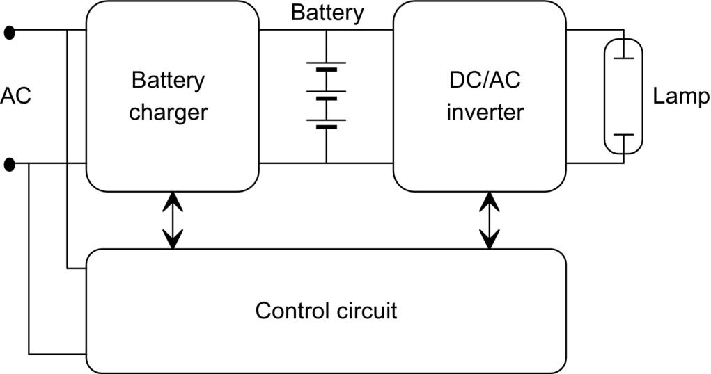
Emergency lightings are used to provide a minimum lighting level in case of a main supply cutoff. Batteries are employed to store energy from the mains and to supply the lamp in case of a main supply failure. A typical block diagram is shown in Fig. 21.34. An ac-dc converter is used as a battery charger to store energy during normal line operation. A control circuit continuously measures the line voltage and activates the inverter in case of a main supply failure. Normally, a minimum operating time of 1 h is required for the system in emergency state. Thus, the use of highly efficient electronic ballasts is mandatory to reduce the battery size and cost. Typical topologies used include class E inverters, push-pull resonant inverters, and half-bridge resonant inverters. Fluorescent lamps are mainly used in emergency ballasts, but high-intensity discharge lamps, such as metal halide lamps or high-pressure sodium lamps, are also used in some special applications.
21.6.3 Automotive Lighting
Electronic ballasts are used in automotive applications such as automobiles, buses, trains, and aircrafts. Normally, a low-voltage dc bus is available to supply the lamps. These applications are similar to portable and emergency lightings previously commented. In modern aircrafts, a 120/208 V, 400 Hz, three-phase electric system is also available and can be employed for lighting. Fluorescent lamps are typically used for automotive indoor lighting, whereas high-intensity discharge lamps are preferred in the exterior lighting, for example, in automobile headlights.
21.6.4 Home and Industrial Lighting
Electronic ballasts, especially for fluorescent lamps, are also very often used in home and industrial applications. The higher efficiency of fluorescent lamps supplied at high frequency provides an interesting energy saving when compared with incandescent lamps. A typical application is the use of compact fluorescent lamps with the electronic ballast inside the lamp base, which can directly substitute an incandescent lamp reducing the energy consumption four or five times. A self-oscillating half-bridge inverter is typically used in these energy saving lamps, since it allows to reduce the size and cost. The power of these lamps is normally below 25 W.
Other applications for higher power include more developed ballasts based on a power factor correction stage followed by a resonant inverter. Hot-cathode fluorescent lamps are mostly used in these electronic ballasts. Also, with the development of modern HID lamps such as metal halide lamps and very-high-pressure sodium lamps (both showing very good color rendition), the use of HID lamps is being more and more frequent in home, commercial, and industrial lighting.
21.6.5 Microprocessor-Based Lighting
The use of microprocessors in combination with electronic ballasts is very interesting from the point of view of energy saving [28–30]. The inclusion of microprocessor circuits allows to incorporate control strategies for dimming, such as scheduling, task tuning, and daylighting [31]. Using these strategies, the achieved energy saving can be as high as 35%–40%. Another advantage of using microprocessors is the possibility of detecting lamp failure or bad operation, thus increasing the reliability and decreasing the maintenance cost of the installation. Most advanced electronic ballasts can include a communication stage to send and receive information regarding the state of the lighting to or from a central control unit. In some cases, communications can be performed via power line, thus reducing the installation costs. Fig. 21.35 shows the block diagram of a microprocessor-based electronic ballast.