
Diode Rectifiers
Yim-Shu Lee The Hong Kong Polytechnic University, Hung Hom, Hong Kong
Martin H.L. Chow The Hong Kong Polytechnic University, Hung Hom, Hong Kong
Abstract
Rectifier circuits are commonly found in all types of electronic systems. The function of a rectifier circuit is to convert an ac voltage into a dc voltage as part of a power supply. Traditionally, the ac voltage is usually a single-phase or polyphase voltage at mains’ frequency. However in some modern applications, e.g., switching regulators, the ac voltage can also be a nonsinusoidal waveform at a frequency of more than 100 kHz.
Keywords
Single-phase rectifier circuits; Three-phase rectifier circuits; Polyphase rectifier circuits; High-frequency rectifier circuits
7.1 Introduction
This chapter describes the application and design of diode rectifier circuits. It covers single-phase rectifier circuits, three-phase rectifier circuits, polyphase rectifier circuits, and high-frequency rectifier circuits. The objectives of this chapter are the following:
• To enable the readers to understand the operation of typical rectifier circuits
• To enable the readers to appreciate the different qualities of rectifiers required for different applications
• To enable the reader to design practical rectifier circuits
The high-frequency rectifier waveforms given are obtained from PSpice simulations, which take into account the secondary effects of stray and parasitic components. In this way, the waveforms can closely resemble the real ones. These waveforms are particularly useful to help designers determine the practical voltage, current, and other ratings of high-frequency rectifiers.
7.2 Single-Phase Diode Rectifiers
There are two types of single-phase diode rectifier that convert a single-phase ac supply into a dc voltage, namely, single-phase half-wave rectifiers and single-phase full-wave rectifiers. In the following subsections, the operations of these rectifier circuits are examined, and their performances are analyzed and compared in a tabulated form. For the sake of simplicity, the diodes are considered to be ideal, that is, they have zero forward voltage drop and reverse recovery time. This assumption is generally valid for the case of diode rectifiers that use the mains, a low-frequency source, as the input and when the forward voltage drop is small compared with the peak voltage of the mains. Furthermore, it is assumed that the load is purely resistive such that the load voltage and the load current have similar waveforms. In Section 7.5, Filtering Systems in Rectifiers Circuits, the effects of inductive load and capacitive load on a diode rectifier are considered in detail.
7.2.1 Single-Phase Half-Wave Rectifiers
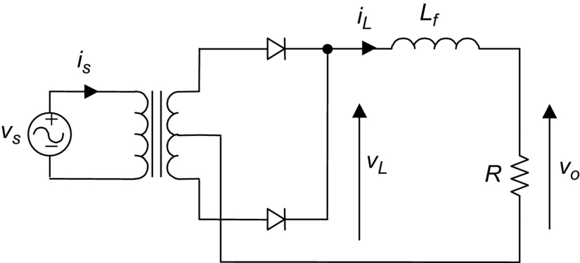
The simplest single-phase diode rectifier is the single-phase half-wave rectifier. A single-phase half-wave rectifier with resistive load is shown in Fig. 7.1. The circuit consists of only one diode that is usually fed with a secondary transformer as shown. During the positive half cycle of the transformer secondary voltage, diode D conducts. During the negative half cycle, diode D stops conducting. Assuming that the transformer has zero internal impedance and provides perfect sinusoidal voltage on its secondary winding, the voltage and current waveforms of resistive load R and the voltage waveform of diode D are shown in Fig. 7.2.
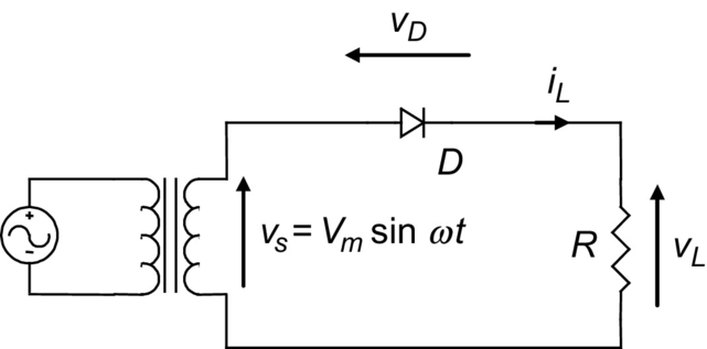
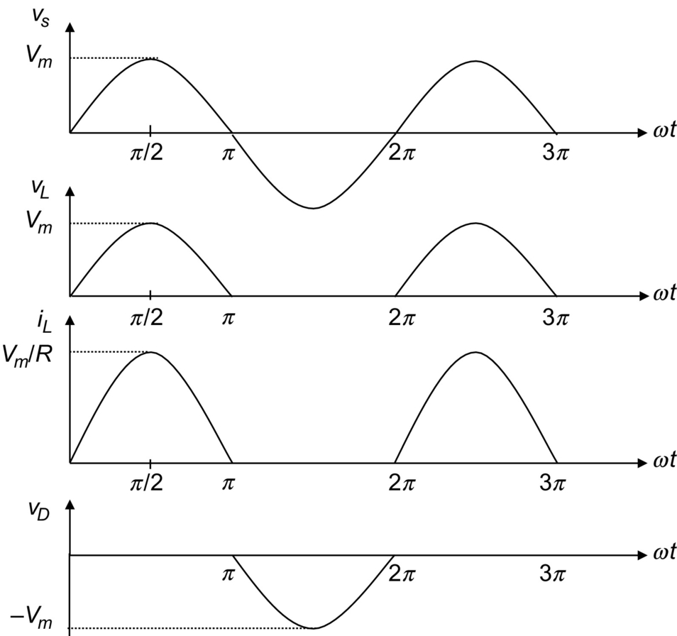
By observing the voltage waveform of diode D in Fig. 7.2, it is clear that the peak inverse voltage (PIV) of diode D is equal to Vm during the negative half cycle of the transformer secondary voltage. Hence, the peak repetitive reverse voltage (VRRM) rating of diode D must be chosen to be higher than Vm to avoid reverse breakdown. In the positive half cycle of the transformer secondary voltage, diode D has a forward current that is equal to the load current; therefore, the peak repetitive forward current (IFRM) rating of diode D must be chosen to be higher than the peak load current, Vm/R, in practice. In addition, the transformer has to carry a dc current that may result in a dc saturation problem of the transformer core.
7.2.2 Single-Phase Full-Wave Rectifiers
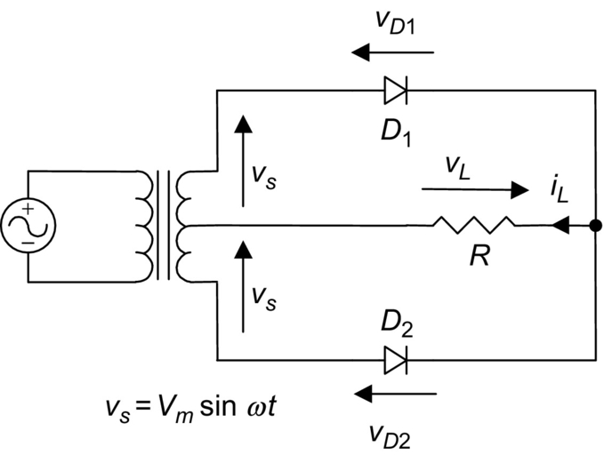
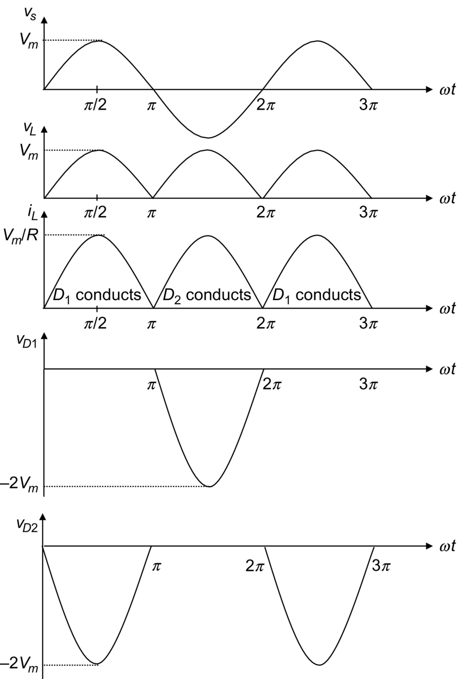
There are two types of single-phase full-wave rectifier, namely, full-wave rectifiers with center-tapped transformer and bridge rectifiers. A full-wave rectifier with a center-tapped transformer is shown in Fig. 7.3. It is clear that each diode, together with the associated half of the transformer, acts as a half-wave rectifier. The outputs of the two half-wave rectifiers are combined to produce full-wave rectification in the load. As far as the transformer is concerned, the dc currents of the two half-wave rectifiers are equal and opposite, such that there is no dc current for creating a transformer core saturation problem. The voltage and current waveforms of the full-wave rectifier are shown in Fig. 7.4. By observing diode voltage waveforms vD1![]() and vD2
and vD2![]() in Fig. 7.4, it is clear that the PIV of the diodes is equal to 2Vm during their blocking state. Hence, the VRRM rating of the diodes must be chosen to be higher than 2Vm to avoid reverse breakdown. (Note that, compared with the half-wave rectifier shown in Fig. 7.1, the full-wave rectifier has twice the dc output voltage, as shown in Section 7.2.4.) During its conducting state, each diode has a forward current which is equal to the load current; therefore, the IFRM rating of these diodes must be chosen to be higher than the peak load current, Vm/R, in practice.
in Fig. 7.4, it is clear that the PIV of the diodes is equal to 2Vm during their blocking state. Hence, the VRRM rating of the diodes must be chosen to be higher than 2Vm to avoid reverse breakdown. (Note that, compared with the half-wave rectifier shown in Fig. 7.1, the full-wave rectifier has twice the dc output voltage, as shown in Section 7.2.4.) During its conducting state, each diode has a forward current which is equal to the load current; therefore, the IFRM rating of these diodes must be chosen to be higher than the peak load current, Vm/R, in practice.
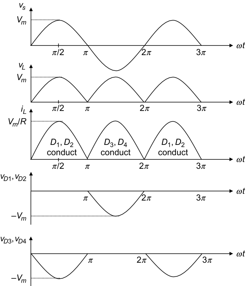
Employing four diodes instead of two, a bridge rectifier as shown in Fig. 7.5 can provide full-wave rectification without using a center-tapped transformer. During the positive half cycle of the transformer secondary voltage, the current flows to the load through diodes D1 and D2. During the negative half cycle, D3 and D4 conduct. The voltage and current waveforms of the bridge rectifier are shown in Fig. 7.6. As with the full-wave rectifier with center-tapped transformer, the IFRM rating of the employed diodes must be chosen to be higher than the peak load current, Vm/R. However, the PIV of the diodes is reduced from 2Vm to Vm during their blocking state.

7.2.3 Performance Parameters
In this subsection, the performance of the rectifiers mentioned above will be evaluated in terms of the following parameters.
7.2.3.1 Voltage Relationships
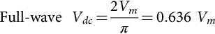
The average value of the load voltage vL is Vdc and it is defined as
Vdc=1T∫T0vL(t)dt
In the case of a half-wave rectifier, Fig. 7.2 indicates that load voltage vL(t)=0![]() for the negative half cycle. Note that the angular frequency of the source ω=2π/T
for the negative half cycle. Note that the angular frequency of the source ω=2π/T![]() , and Eq. (7.1) can be rewritten as
, and Eq. (7.1) can be rewritten as
Vdc=12π∫π0Vmsinωtd(ωt)
Therefore,
Half-waveVdc=Vmπ=0.318Vm
In the case of a full-wave rectifier, Figs. 7.4 and 7.6 indicate that vL(t)=Vm|sinωt|![]() for both the positive and negative half cycles. Hence, Eq. (7.1) can be rewritten as
for both the positive and negative half cycles. Hence, Eq. (7.1) can be rewritten as
Vdc=1π∫π0Vmsinωtd(ωt)
Therefore,
Full-waveVdc=2Vmπ=0.636Vm
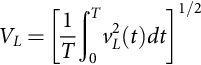
The root-mean-square (rms) value of load voltage vL is VL, which is defined as
VL=[1T∫T0v2L(t)dt]1/2
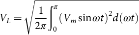
In the case of a half-wave rectifier, vL(t)=0![]() for the negative half cycle; therefore, Eq. (7.6) can be rewritten as
for the negative half cycle; therefore, Eq. (7.6) can be rewritten as
VL=√12π∫π0(Vmsinωt)2d(ωt)
or
Half-waveVL=Vm2=0.5Vm
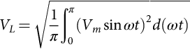
In the case of a full-wave rectifier, vL(t)=Vm|sinωt|![]() for both the positive and negative half cycles. Hence, Eq. (7.6) can be rewritten as
for both the positive and negative half cycles. Hence, Eq. (7.6) can be rewritten as
VL=√1π∫π0(Vmsinωt)2d(ωt)
or
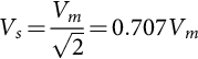
Full-waveVL=Vm√2=0.707Vm
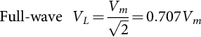
The result of Eq. (7.10) is as expected because the rms value of a full-wave rectified voltage should be equal to that of the original ac voltage.
7.2.3.2 Current Relationships
The average value of load current iL is Idc, and because load R is purely resistive, it can be found as
Idc=VdcR
The rms value of load current iL is IL, and it can be found as
IL=VLR
In the case of a half-wave rectifier, from Eq. (7.3),
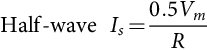
Half-waveIdc=0.318VmR
and from Eq. (7.8),
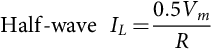
Half-waveIL=0.5VmR
In the case of a full-wave rectifier, from Eq. (7.5),
Full-waveIdc=0.636VmR
and from Eq. (7.10),
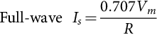
Full-waveIL=0.707VmR
7.2.3.3 Rectification Ratio
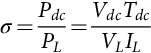
The rectification ratio, which is a figure of merit for comparing the effectiveness of rectification, is defined as
σ=PdcPL=VdcTdcVLIL
In the case of a half-wave diode rectifier, the rectification ratio can be determined by substituting Eqs. (7.3), (7.13), (7.8), and (7.14) into Eq. (7.17):
Half-waveσ=(0.318Vm)2(0.5Vm)2=40.5%

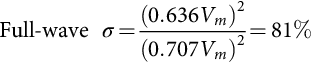
In the case of a full-wave rectifier, the rectification ratio is obtained by substituting Eqs. (7.5), (7.15), (7.10), and (7.16) into Eq. (7.17):
Full-waveσ=(0.636Vm)2(0.707Vm)2=81%
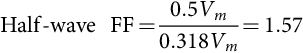
7.2.3.4 Form Factor
The form factor (FF) is defined as the ratio of the root-mean-square value (heating component) of a voltage or current to its average value:
FF=VLVdcorILIdc
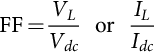
Half-waveFF=0.5Vm0.318Vm=1.57
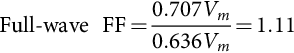
In the case of a full-wave rectifier, the FF can be found by substituting Eqs. (7.16) and (7.15) into Eq. (7.20):
Full-waveFF=0.707Vm0.636Vm=1.11
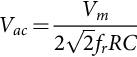
7.2.3.5 Ripple Factor
The ripple factor (RF), which is a measure of the ripple content, is defined as
RF=VacVdc

where Vac is the effective (rms) value of the ac component of load voltage vL:
Vac=√V2L−V2dc
Substituting Eq. (7.24) into Eq. (7.23), the RF can be expressed as
RF=√(VLVdc)2−1=√FF2−1

In the case of a half-wave rectifier,
Half-waveRF=√1.572−1=1.21
In the case of a full-wave rectifier,
Full-waveRF=√1.112−1=0.482
7.2.3.6 Transformer Utilization Factor
The transformer utilization factor (TUF), which is a measure of the merit of a rectifier circuit, is defined as the ratio of the dc output power to the transformer volt-ampere (VA) rating required by the secondary winding:
TUF=PdcVsIs=VdcIdcVsIs
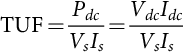
where Vs and Is are the rms voltage and rms current ratings of the secondary transformer:
Vs=Vm√2=0.707Vm
The rms value of the transformer secondary current Is is the same as that of the load current IL. For a half-wave rectifier, Is can be found from Eq. (7.14):
Half-waveIs=0.5VmR
For a full-wave rectifier, Is is found from Eq. (7.16):
Full-waveIs=0.707VmR
Therefore, the TUF of a half-wave rectifier can be obtained by substituting Eqs. (7.3), (7.13), (7.29), and (7.30) into Eq. (7.28):
Half-waveTUF=0.31820.707×0.5=0.286
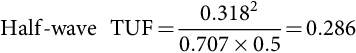
The poor TUF of a half-wave rectifier signifies that the transformer employed must have a 3.496 (1/0.286) VA rating in order to deliver 1 W dc output power to the load. In addition, the transformer secondary winding has to carry a dc current that may cause magnetic core saturation. As a result, half-wave rectifiers are used only when the current requirement is small.
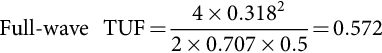
In the case of a full-wave rectifier with center-tapped transformer, the circuit can be treated as two half-wave rectifiers operating together. Therefore, the transformer secondary VA rating, VsIs, is double that of a half-wave rectifier, but the output dc power is increased by a factor of four due to higher rectification ratio as indicated by Eqs. (7.5) and (7.15). Therefore, the TUF of a full-wave rectifier with center-tapped transformer can be found from Eq. (7.32):
Full-waveTUF=4×0.31822×0.707×0.5=0.572
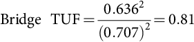
In the case of a bridge rectifier, it has the highest TUF in single-phase rectifier circuits because the currents flowing in both the primary and secondary windings are continuous sinewaves. By substituting Eqs. (7.5), (7.15), (7.29), and (7.31) into Eq. (7.28), the TUF of a bridge rectifier can be found:
BridgeTUF=0.6362(0.707)2=0.81
The transformer primary VA rating of a full-wave rectifier is equal to that of a bridge rectifier since the current flowing in the primary winding is also a continuous sinewave.
7.2.3.7 Harmonics
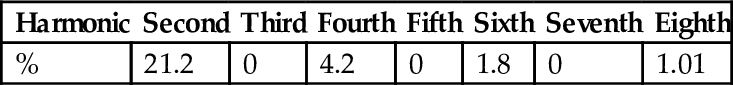
Full-wave rectifier circuits with resistive load do not produce harmonic currents in their transformers. In half-wave rectifiers, harmonic currents are generated. The amplitudes of the harmonic currents of a half-wave rectifier with resistive load, relative to the fundamental, are given in Table 7.1. The extra loss caused by the harmonics in the resistive loaded rectifier circuits is often neglected because it is not high compared with other losses. However, with nonlinear loads, harmonics can cause appreciable loss and other problems such as poor power factor and interference.
7.2.4 Design Considerations
In a practical design, the goal is to achieve a given dc output voltage. Therefore, it is more convenient to put all the design parameters in terms of Vdc. For example, the rating and turn ratio of the transformer in a rectifier circuit can be easily determined if the rms input voltage to the rectifier is in terms of the required output voltage Vdc.
Denote the rms value of the input voltage to the rectifier as Vs, which is equal to 0.707Vm. Based on this relation and Eq. (7.3), the rms input voltage to a half-wave rectifier is found as
Half-waveVs=2.22Vdc
Similarly, from Eqs. (7.5) and (7.29), the rms input voltage per secondary winding of a full-wave rectifier is found as
Full-waveVs=1.11Vdc
Another important design parameter is the VRRM rating of the diodes employed.
In the case of a half-wave rectifier, from Eq. (7.3),
Half-waveVRRM=Vm=Vdc0.318=3.14Vdc

In the case of a full-wave rectifier with center-tapped transformer, from Eq. (7.5),
Full-waveVRRM=2Vm=2Vdc0.636=3.14Vdc

In the case of a bridge rectifier, also from Eq. (7.5),
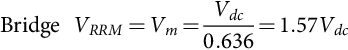
BridgeVRRM=Vm=Vdc0.636=1.57Vdc
It is important to evaluate the IFRM rating of the employed diodes in rectifier circuits.
In the case of a half-wave rectifier, from Eq. (7.13),
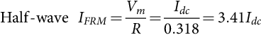
Half-waveIFRM=VmR=Idc0.318=3.41Idc
In the case of full-wave rectifiers, from Eq. (7.15),
Full-waveIFRM=VmR=Idc0.636=1.57Idc

The important design parameters of basic single-phase rectifier circuits with resistive loads are summarized in Table 7.2.
Table 7.2
Important design parameters of basic single-phase rectifier circuits with resistive load
| Half-wave rectifier | Full-wave rectifier with center-tapped transformer | Full-wave bridge rectifier | |
| Peak repetitive reverse voltage VRRM | 3.14Vdc | 3.14Vdc | 1.57Vdc |
| RMS input voltage per transformer leg Vs | 2.22Vdc | 1.11Vdc | 1.11Vdc |
| Diode average current IF(AV) | 1.00Idc | 0.50Idc | 0.50Idc |
| Peak repetitive forward current IFRM | 3.14IF(AV) | 1.57IF(AV) | 1.57IF(AV) |
| Diode rms current IF(RMS) | 1.57Idc | 0.785Idc | 0.785Idc |
| Form factor of diode current IF(RMS)/IF(AV) | 1.57 | 1.57 | 1.57 |
| Rectification ratio | 0.405 | 0.81 | 0.81 |
| Form factor | 1.57 | 1.11 | 1.11 |
| Ripple factor | 1.21 | 0.482 | 0.482 |
| Transformer rating primary VA | 2.69Pdc | 1.23Pdc | 1.23Pdc |
| Transformer rating secondary VA | 3.49Pdc | 1.75Pdc | 1.23Pdc |
| Output ripple frequency fr | 1fi | 2fi | 2fi |

7.3 Three-Phase Diode Rectifiers
It has been shown in Section 7.2 that single-phase diode rectifiers require a rather high transformer VA rating for a given dc output power. Therefore, these rectifiers are suitable only for low-to-medium power applications. For power output higher than 15 kW, three-phase or polyphase diode rectifiers should be employed. There are two types of three-phase diode rectifier that convert a three-phase ac supply into a dc voltage, namely, star rectifiers and bridge rectifiers. In the following subsections, the operations of these rectifiers are examined, and their performances are analyzed and compared in tabulated form. For the sake of simplicity, the diodes and the transformers are considered to be ideal, that is, the diodes have zero forward voltage drop and reverse current and the transformers possess no resistance and no leakage inductance. Furthermore, it is assumed that the load is purely resistive, such that the load voltage and the load current have similar waveforms. In Section 7.5, Filtering Systems in Rectifier Circuits, the effects of inductive load and capacitive load on a diode rectifier are considered in detail.
7.3.1 Three-Phase Star Rectifiers
7.3.1.1 Basic Three-Phase Star Rectifier Circuit
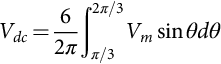
A basic three-phase star rectifier circuit is shown in Fig. 7.7. This circuit can be considered as three single-phase half-wave rectifiers combined together. Therefore, it is sometimes referred to as a three-phase half-wave rectifier. The diode in a particular phase conducts during the period when the voltage on that phase is higher than that on the other two phases. The voltage waveforms of each phase and the load are shown in Fig. 7.8. It is clear that, unlike the single-phase rectifier circuit, the conduction angle of each diode is 2π/3, instead of π. This circuit finds uses where the required dc output voltage is relatively low, and the required output current is too large for a practical single-phase system.
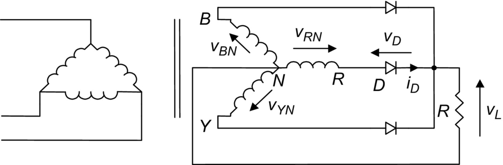

Taking phase R as an example, diode D conducts from π/6 to 5π/6. Therefore, using Eq. (7.1), the average value of the output can be found as
Vdc=32π∫5π/6π/6Vmsinθdθ
or
Vdc=Vm3π√32=0.827Vm
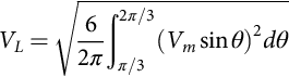
Similarly, using Eq. (7.6), the rms value of the output voltage can be found as
VL=√32π∫5π/6π/6(Vmsinθ)2dθ

or
VL=Vm√32π(π3+√34)=0.84Vm

In addition, the rms current in each transformer secondary winding can also be found as
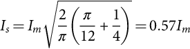
Is=Im√12π(π3+√34)=0.485Im

where Im=Vm/R![]() .
.
Based on the relationships stated in Eqs. (7.43), (7.45), (7.46), all the important design parameters of the three-phase star rectifier can be evaluated, as listed in Table 7.3, which is given at the end of Section 7.3.2. Note that, as with a single-phase half-wave rectifier, the three-phase star rectifier shown in Fig. 7.7 has direct currents in the secondary windings that can cause a transformer core saturation problem. In addition, the currents in the primary do not sum to zero. Therefore, it is preferable not to have star-connected primary windings.
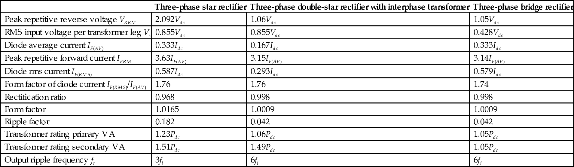
Table 7.3
Important design parameters of the three-phase rectifier circuits with the resistive load
| Three-phase star rectifier | Three-phase double-star rectifier with interphase transformer | Three-phase bridge rectifier | |
| Peak repetitive reverse voltage VRRM | 2.092Vdc | 1.06Vdc | 1.05Vdc |
| RMS input voltage per transformer leg Vs | 0.855Vdc | 0.855Vdc | 0.428Vdc |
| Diode average current IF(AV) | 0.333Idc | 0.167Idc | 0.333Idc |
| Peak repetitive forward current IFRM | 3.63IF(AV) | 3.15IF(AV) | 3.14IF(AV) |
| Diode rms current IF(RMS) | 0.587Idc | 0.293Idc | 0.579Idc |
| Form factor of diode current IF(RMS)/IF(AV) | 1.76 | 1.76 | 1.74 |
| Rectification ratio | 0.968 | 0.998 | 0.998 |
| Form factor | 1.0165 | 1.0009 | 1.0009 |
| Ripple factor | 0.182 | 0.042 | 0.042 |
| Transformer rating primary VA | 1.23Pdc | 1.06Pdc | 1.05Pdc |
| Transformer rating secondary VA | 1.51Pdc | 1.49Pdc | 1.05Pdc |
| Output ripple frequency fr | 3fi | 6fi | 6fi |
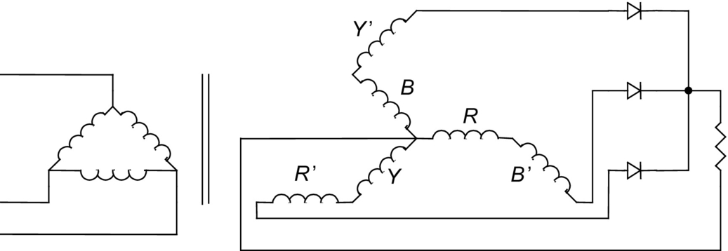
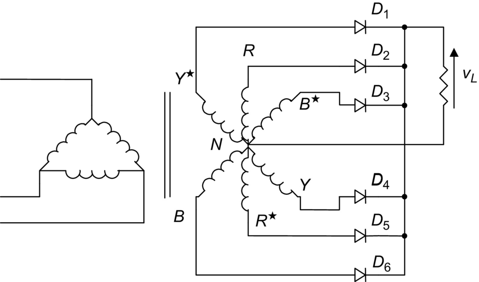
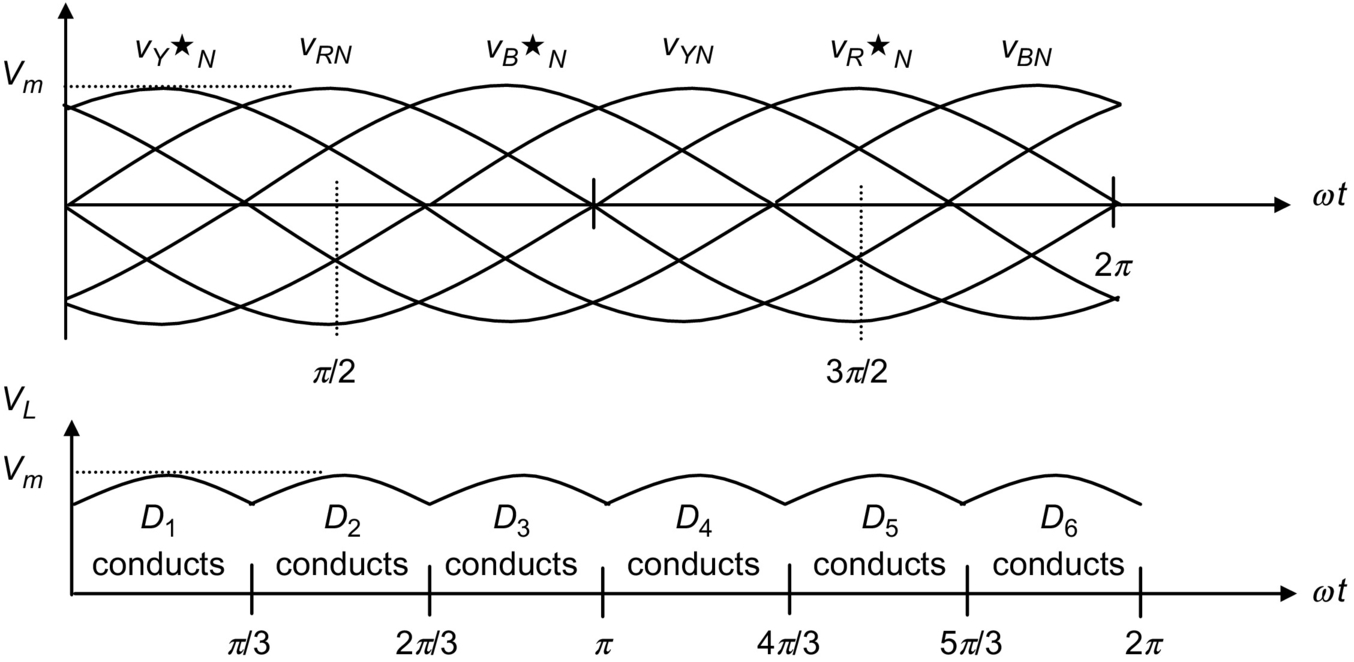
7.3.1.2 Three-Phase Interstar Rectifier Circuit
The transformer core saturation problem in the three-phase star rectifier can be avoided by a special arrangement in its secondary windings, known as zigzag connection. The modified circuit is called the three-phase interstar or zigzag rectifier circuit, as shown in Fig. 7.9. Each secondary-phase voltage is obtained from two equal-voltage secondary windings (with a phase displacement of π/3) connected in series so that the dc magnetizing forces due to the two secondary windings on any limb are equal and opposite. At the expense of extra secondary windings (increasing the transformer secondary rating factor from 1.51 to 1.74 VA/W), this circuit connection eliminates the effects of core saturation and reduces the transformer primary rating factor to the minimum of 1.05 VA/W. Apart from transformer ratings, all the design parameters of this circuit are the same as those of a three-phase star rectifier (therefore not separately listed in Table 7.3). Furthermore, a star-connected primary winding with no neutral connection is equally permissible because the sum of all primary phase currents is zero at all times.
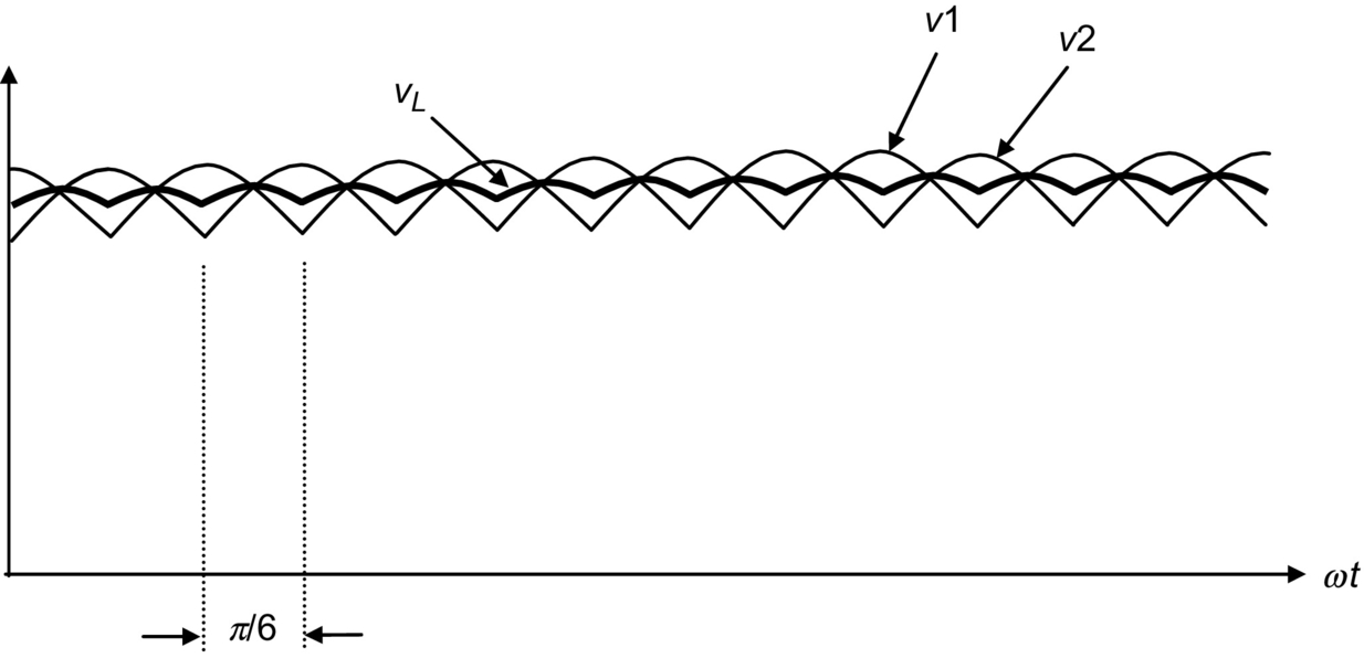
7.3.1.3 Three-Phase Double-Star Rectifier With Interphase Transformer
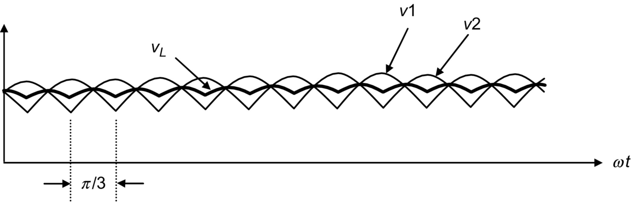
This circuit consists essentially of two three-phase star rectifiers with their neutral points interconnected through an interphase transformer or reactor (Fig. 7.10). The polarities of the corresponding secondary windings in the two interconnected systems are reversed with respect to each other, so that the rectifier output voltage of one three-phase unit is at a minimum when the rectifier output voltage of the other unit is at a maximum as shown in Fig. 7.11. The function of the interphase transformer is to cause the output voltage vL to be the average of the rectified voltages v1 and v2 as shown in Fig. 7.11. In addition, the ripple frequency of the output voltage is now six times that of the mains, and therefore, the component size of the filter (if there is any) becomes smaller. In a balanced circuit, the output currents of two three-phase units flowing in opposite directions in the interphase transformer winding will produce no dc magnetization current. Similarly, the dc magnetization currents in the secondary windings of two three-phase units cancel each other out.
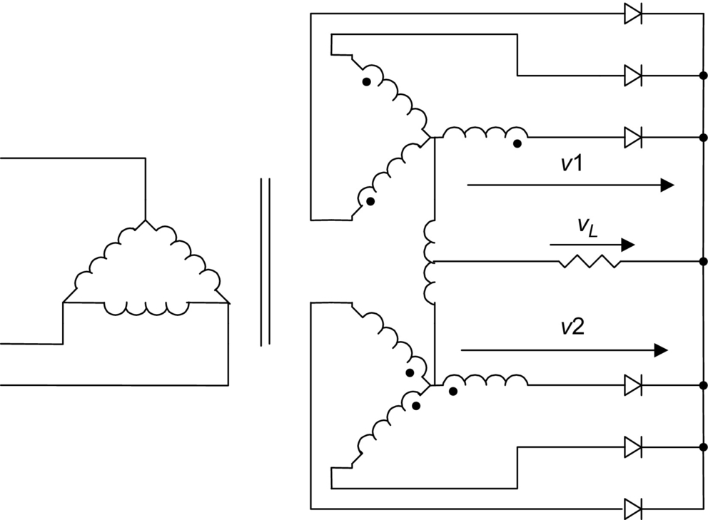
By virtue of the symmetry of the secondary circuits, the three primary currents add up to zero at all times. Therefore, a star primary winding with no neutral connection would be equally permissible.
7.3.2 Three-Phase Bridge Rectifiers
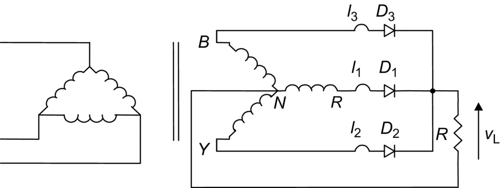
Three-phase bridge rectifiers are commonly used for high-power applications because they have the highest possible transformer utilization factor for a three-phase system. The circuit of a three-phase bridge rectifier is shown in Fig. 7.12. The diodes are numbered in the order of conduction sequences, and the conduction angle of each diode is 2π/3.
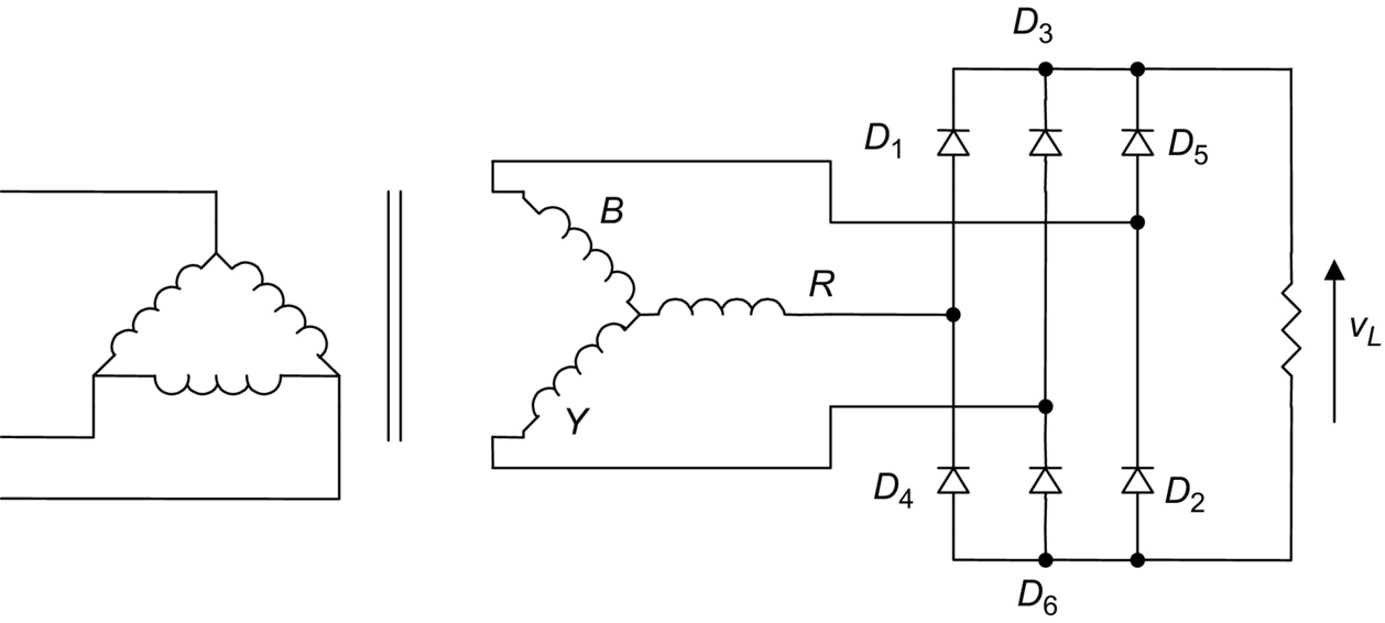
The conduction sequence for diodes is 12, 23, 34, 45, 56, and 61. The voltage and the current waveforms of the three-phase bridge rectifier are shown in Fig. 7.13. The line voltage is 1.73 times the phase voltage of a three-phase star-connected source. It is permissible to use any combination of star- or delta-connected primary and secondary windings because the currents associated with the secondary windings are symmetrical.
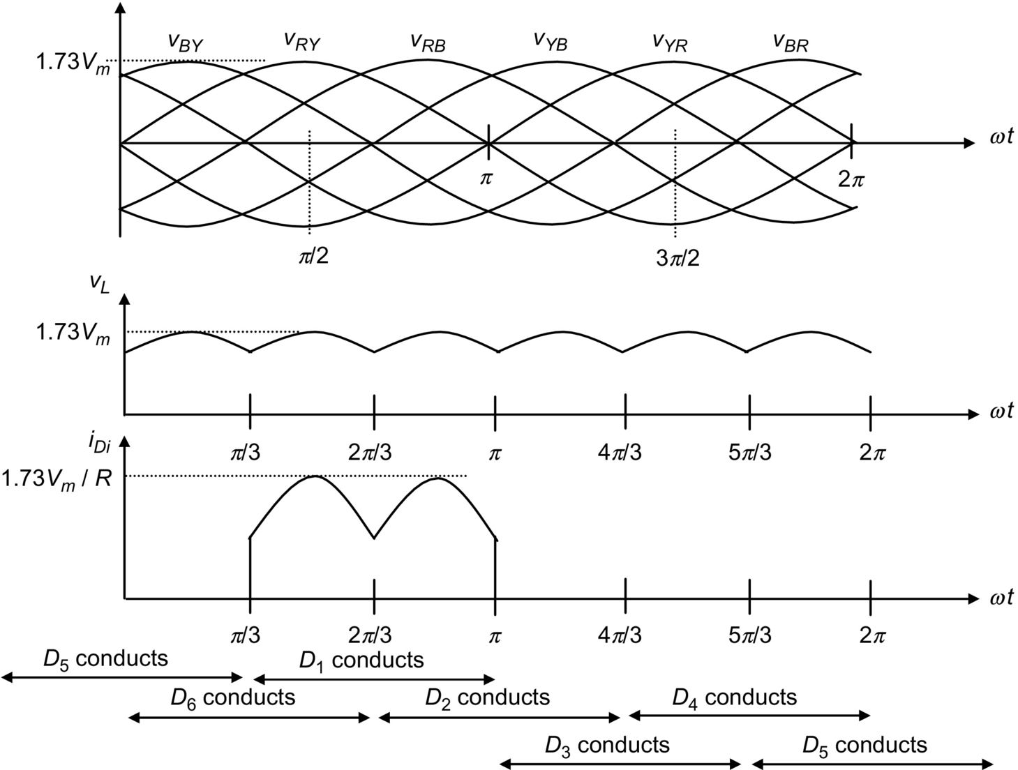
Using Eq. (7.1), the average value of the output can be found as
Vdc=62π∫2π/3π/3√3Vmsinθdθ
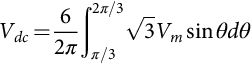
or
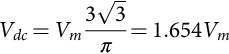
Vdc=Vm3√3π=1.654Vm
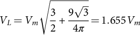
Similarly, using Eq. (7.6), the rms value of the output voltage can be found as
VL=√9π∫2π/3π/3(Vmsinθ)2dθ
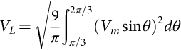
or
VL=Vm√32+9√34π=1.655Vm
In addition, the rms current in each transformer secondary winding can also be found as
Is=Im√2π(π6+√34)=0.78Im

and the rms current through a diode is
ID=Im√1π(π6+√34)=0.552Im
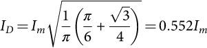
where Im=1.73Vm/R![]() .
.
Based on Eqs. (7.48), (7.50), (7.51), (7.52), all the important design parameters of the three-phase star rectifier can be evaluated, as listed in Table 7.3. The dc output voltage is slightly lower than the peak line voltage or 2.34 times the rms phase voltage. The VRRM rating of the employed diodes is 1.05 times the dc output voltage, and the IFRM rating of the employed diodes is 0.579 times the dc output current. Therefore, this three-phase bridge rectifier is very efficient and popular wherever both dc voltage and current requirements are high. In many applications, no additional filter is required because the output ripple voltage is only 4.2%. Even if a filter is required, the size of the filter is relatively small because the ripple frequency is increased to six times the input frequency.
7.3.3 Operation of Rectifiers With Finite Source Inductance
It has been assumed in the preceding sections that the commutation of current from one diode to the next takes place instantaneously when the interphase voltage assumes the necessary polarity. In practice, this is hardly possible because there are finite inductances associated with the source. For the purpose of discussing the effects of the finite source inductance, a three-phase star rectifier with transformer leakage inductances is shown in Fig. 7.14, where l1, l2, and l3 denote the leakage inductances associated with the transformer secondary windings.
Refer to Fig. 7.15. At the time when vYN is about to become larger than vRN, due to leakage inductance l1, the current in D1 cannot fall to zero immediately. Similarly, due to the leakage inductance l2, the current in D2 cannot increase immediately to the full value. The result is that both the diodes conduct for a certain period, which is called the overlap (or commutation) angle. The overlap reduces the rectified voltage vL as shown in the upper voltage waveform of Fig. 7.15. If all the leakage inductances are equal, that is, l1=l2=l3=lc![]() , then the amount of reduction of dc output voltage can be estimated as mfilcIdc, where m is the ratio of the lowest ripple frequency to the input frequency.
, then the amount of reduction of dc output voltage can be estimated as mfilcIdc, where m is the ratio of the lowest ripple frequency to the input frequency.

For example, for a three-phase star rectifier operating from a 60 Hz supply with an average load current of 50 A, the amount of reduction of the dc output voltage is 2.7 V if the leakage inductance in each secondary winding is 300 μH.
7.4 Poly-Phase Diode Rectifiers
7.4.1 Six-Phase Star Rectifier
A basic six-phase star rectifier circuit is shown in Fig. 7.16. The six-phase voltages on the secondary are obtained by means of a center-tapped arrangement on a star-connected three-phase winding. Therefore, it is sometimes referred to as a three-phase full-wave rectifier. The diode in a particular phase conducts during the period when the voltage on that phase is higher than that on the other phases. The voltage waveforms of each phase and the load are shown in Fig. 7.17. It is clear that, unlike the three-phase star rectifier circuit, the conduction angle of each diode is π/3, instead of 2π/3. Currents flow in only one rectifying element at a time, resulting in a low average current, but a high peak to an average current ratio in the diodes and poor transformer secondary utilization. Nevertheless, the dc currents in the secondary of the six-phase star rectifier cancel in the secondary windings like a full-wave rectifier and, therefore, core saturation is not encountered. This six-phase star circuit is attractive in applications that require a low ripple factor and a common cathode or anode for the rectifiers.
By considering the output voltage provided by vRN between π/3 and 2π/3, the average value of the output voltage can be found as
Vdc=62π∫2π/3π/3Vmsinθdθ
or
Vdc=Vm6π12=0.955Vm
Similarly, the rms value of the output voltage can be found as
VL=√62π∫2π/3π/3(Vmsinθ)2dθ
or
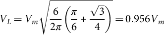
VL=Vm√62π(π6+√34)=0.956Vm
In addition, the rms current in each transformer secondary winding can also be found as
Is=Im√12π(π6+√34)=0.39Im

where Im=Vm/R![]() .
.
Based on the relationships stated in Eqs. (7.55)–(7.57), all the important design parameters of the six-phase star rectifier can be evaluated, as listed in Table 7.4 (given at the end of Section 7.4.3).
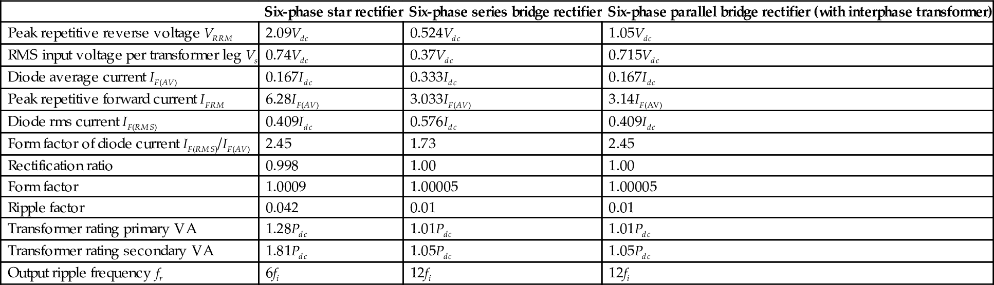
Table 7.4
Important design parameters of the six-phase rectifier circuits with resistive load
| Six-phase star rectifier | Six-phase series bridge rectifier | Six-phase parallel bridge rectifier (with interphase transformer) | |
| Peak repetitive reverse voltage VRRM | 2.09Vdc | 0.524Vdc | 1.05Vdc |
| RMS input voltage per transformer leg Vs | 0.74Vdc | 0.37Vdc | 0.715Vdc |
| Diode average current IF(AV) | 0.167Idc | 0.333Idc | 0.167Idc |
| Peak repetitive forward current IFRM | 6.28IF(AV) | 3.033IF(AV) | 3.14IF(AV) |
| Diode rms current IF(RMS) | 0.409Idc | 0.576Idc | 0.409Idc |
| Form factor of diode current IF(RMS)/IF(AV) | 2.45 | 1.73 | 2.45 |
| Rectification ratio | 0.998 | 1.00 | 1.00 |
| Form factor | 1.0009 | 1.00005 | 1.00005 |
| Ripple factor | 0.042 | 0.01 | 0.01 |
| Transformer rating primary VA | 1.28Pdc | 1.01Pdc | 1.01Pdc |
| Transformer rating secondary VA | 1.81Pdc | 1.05Pdc | 1.05Pdc |
| Output ripple frequency fr | 6fi | 12fi | 12fi |
7.4.2 Six-Phase Series Bridge Rectifier
The star- and delta-connected secondaries have an inherent π/6-phase displacement between their output voltages. When a star- and a delta-connected bridge rectifier are connected in series as shown in Fig. 7.18, the combined output voltage will have a doubled ripple frequency (12 times that of the mains). The ripple of the combined output voltage will also be reduced from 4.2% (for each individual bridge rectifier) to 1%. The combined bridge rectifier is referred to as a six-phase series bridge rectifier.
In the six-phase series bridge rectifier shown in Fig. 7.18, let V⁎m![]() be the peak voltage of the delta-connected secondary. The peak voltage between the lines of the star-connected secondary is also V⁎m
be the peak voltage of the delta-connected secondary. The peak voltage between the lines of the star-connected secondary is also V⁎m![]() . The peak voltage across the load, denoted as Vm, is equal to 2V⁎m×cos(π/12)
. The peak voltage across the load, denoted as Vm, is equal to 2V⁎m×cos(π/12)![]() or 1.932V⁎m
or 1.932V⁎m![]() because there is π/6-phase displacement between the secondaries. The ripple frequency is twelve times the mains frequency. The average value of the output voltage can be found as
because there is π/6-phase displacement between the secondaries. The ripple frequency is twelve times the mains frequency. The average value of the output voltage can be found as
Vdc=122π∫7π/125π/12Vmsinθdθ

or
Vdc=Vm12π√3−12√2=0.98862Vm

The rms value of the output voltage can be found as
VL=√122π∫7π/125π/12(Vmsinθ)2dθ

or
VL=Vm√122π(π12+14)=0.98867Vm

The rms current in each transformer secondary winding is
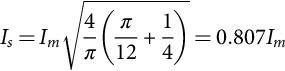
Is=Im√4π(π12+14)=0.807Im
The rms current through a diode is
Is=Im√2π(π12+14)=0.57Im
where Im=Vm/R![]() .
.
Based on Eqs. (7.59), (7.61), (7.62), (7.63), all the important design parameters of the six-phase series bridge rectifier can be evaluated, as listed in Table 7.4 (given at the end of Section 7.4.3).
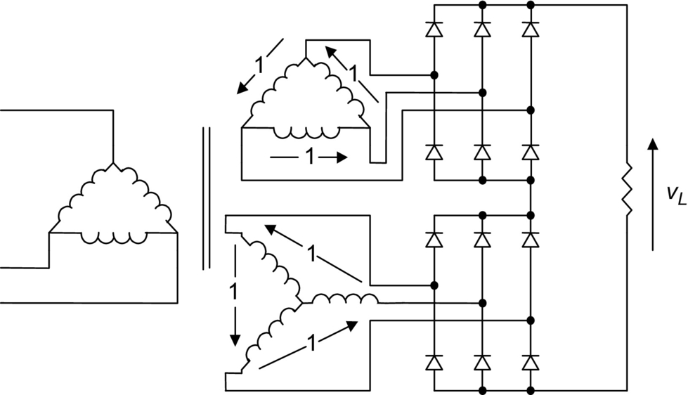
7.4.3 Six-Phase Parallel Bridge Rectifier
The six-phase series bridge rectifier described above is useful for high-output voltage applications. However, for high-output current applications, the six-phase parallel bridge rectifier (with an interphase transformer) shown in Fig. 7.19 should be used.

The function of the interphase transformer is to cause the output voltage vL to be the average of the rectified voltages v1 and v2 as shown in Fig. 7.20. As with the six-phase series bridge rectifier, the output ripple frequency of the six-phase parallel bridge rectifier is also 12 times that of the mains. Further filtering on the output voltage is usually not required. Assuming a balanced circuit, the output currents of two three-phase units (flowing in opposite directions in the interphase transformer winding) produce no dc magnetization current.
All the important design parameters of the six-phase parallel rectifiers with interphase transformer are also listed in Table 7.4.
7.5 Filtering Systems in Rectifier Circuits
Filters are commonly employed in rectifier circuits for smoothing out the dc output voltage of the load. They are classified as inductor-input dc filters and capacitor-input dc filters. Inductor-input dc filters are preferred in high-power applications because more efficient transformer operation is obtained due to the reduction in the form factor of the rectifier current. Capacitor-input dc filters can provide volumetrically efficient operation, but they demand excessive turn-on and repetitive surge currents. Therefore, capacitor-input dc filters are suitable only for lower-power systems where close regulation is usually achieved by an electronic regulator cascaded with the rectifier.
7.5.1 Inductive-Input DC Filters
The simplest inductive-input dc filter is shown in Fig. 7.21A. The output current of the rectifier can be maintained at a steady value if the inductance of Lf is sufficiently large (ωLf≫R)![]() . The filtering action is more effective in heavy load conditions than in light load conditions. If the ripple attenuation is not sufficient even with large values of inductance, an L-section filter as shown in Fig. 7.21B can be used for further filtering. In practice, multiple L-section filters can also be employed if the requirement on the output ripple is very stringent.
. The filtering action is more effective in heavy load conditions than in light load conditions. If the ripple attenuation is not sufficient even with large values of inductance, an L-section filter as shown in Fig. 7.21B can be used for further filtering. In practice, multiple L-section filters can also be employed if the requirement on the output ripple is very stringent.

For a simple inductive-input dc filter shown in Fig. 7.21A the ripple is reduced by the factor
vovL=R√R2+(2πfrLf)2
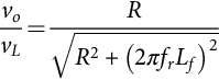
where vL is the ripple voltage before filtering, vo is the ripple voltage after filtering, and fr is the ripple frequency.
For the inductive-input dc filter shown in Fig. 7.21B, the amount of reduction in the ripple voltage can be estimated as
vovL=|11−(2πfr)2LfCf|
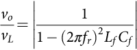
where fr is the ripple frequency, if R≫1/2πfrCf![]() .
.
7.5.1.1 Voltage and Current Waveforms of Full-Wave Rectifier With Inductor-Input DC Filter
Fig. 7.22 shows a single-phase full-wave rectifier with an inductor-input dc filter. The voltage and current waveforms are illustrated in Fig. 7.23.

When the inductance of Lf is infinite, the current through the inductor and the output voltage are constant. When inductor Lf is finite, the current through the inductor has a ripple component, as shown by the dotted lines in Fig. 7.23. If the input inductance is too small, the current decreases to zero (becoming discontinuous) during a portion of the time between the peaks of the rectifier output voltage. The minimum value of inductance required to maintain a continuous current is known as the critical inductance LC.
7.5.1.2 Critical Inductance LC
In the case of single-phase full-wave rectifiers, the critical inductance can be found as
Full-waveLC=R6πfi

where fi is the input mains frequency.
In the case of polyphase rectifiers, the critical inductance can be found as
Poly-phaseLC=R3πm(m2−1)fi
where m is ratio of the lowest ripple frequency to the input frequency, for example, m=6![]() for a three-phase bridge rectifier.
for a three-phase bridge rectifier.
7.5.1.3 Determining the Input Inductance for a Given Ripple Factor
In practice, the choice of the input inductance depends on the required ripple factor of the output voltage. The ripple voltage of a rectifier without filtering can be found by means of Fourier analysis. For example, the coefficient of the nth harmonic component of the rectified voltage vL shown in Fig. 7.22 can be expressed as
vLn=−4Vmπ(n2−1)

where n=2,4,8,…![]() , etc.
, etc.
The dc component of the rectifier voltage is given by Eq. (7.5). Therefore, in addition to Eq. (7.27), the ripple factor can also be expressed as
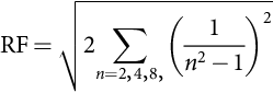
RF=√2∑n=2,4,8,(1n2−1)2
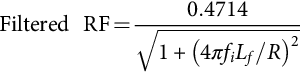
Considering only the lowest-order harmonic (n=2)![]() , the output ripple factor of a simple inductor-input dc filter (without Cf) can be found, from Eqs. (7.64) and (7.69), as
, the output ripple factor of a simple inductor-input dc filter (without Cf) can be found, from Eqs. (7.64) and (7.69), as
FilteredRF=0.4714√1+(4πfiLf/R)2
7.5.1.4 Harmonics of the Input Current
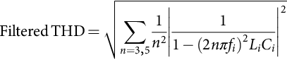
In general, the total harmonic distortion (THD) of an input current is defined as
THD=√(IsIs1)2−1
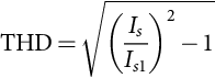
where Is is the rms value of the input current and Is1 and the rms value of the fundamental component of the input current. The THD can also be expressed as
THD=√∑n=2,3,4,(IsnIs1)2
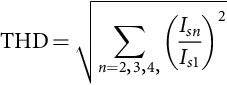
where Isn is the rms value of the nth harmonic component of the input current.
Moreover, the input power factor is defined as
PF=Is1Iscosϕ

where ϕ is the displacement angle between the fundamental components of the input current and voltage.
Assume that inductor Lf of the circuit shown in Fig. 7.22 has an infinitely large inductance. The input current is then a square wave. This input current contains undesirable higher harmonics that reduce the input power factor of the system. The input current can be easily expressed as
is=4Imπ∑n=1,3,5,1nsin2nπfit
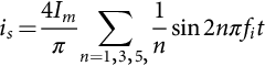
The rms values of the input current and its fundamental component are Im and 4Im/(π√2)![]() , respectively. Therefore, the THD of the input current of this circuit is 0.484. Since the displacement angle is ϕ=0
, respectively. Therefore, the THD of the input current of this circuit is 0.484. Since the displacement angle is ϕ=0![]() , the power factor is 4/(π√2)=0.9.
, the power factor is 4/(π√2)=0.9.![]()
The power factor of the circuit shown in Fig. 7.22 can be improved by installing an ac filter between the source and the rectifier, as shown in Fig. 7.24.

Considering only the harmonic components, the equivalent circuit of the rectifier given in Fig. 7.24 can be found as shown in Fig. 7.25. The rms value of the nth harmonic current appearing in the supply can then be obtained using the current divider rule:
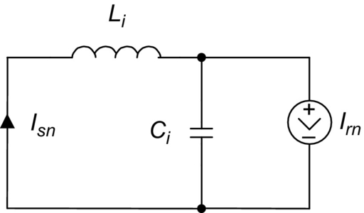
Isn=|11−(2nπfi)2LiCi|Irn

where Irn is the rms value of the nth harmonic current of the rectifier.
Applying Eq. (7.73) and knowing Irn/Ir1=1/n![]() from Eq. (7.74), the THD of the rectifier with input filter shown in Fig. 7.24 can be found as
from Eq. (7.74), the THD of the rectifier with input filter shown in Fig. 7.24 can be found as
FilteredTHD=√∑n=3,51n2|11−(2nπfi)2LiCi|2
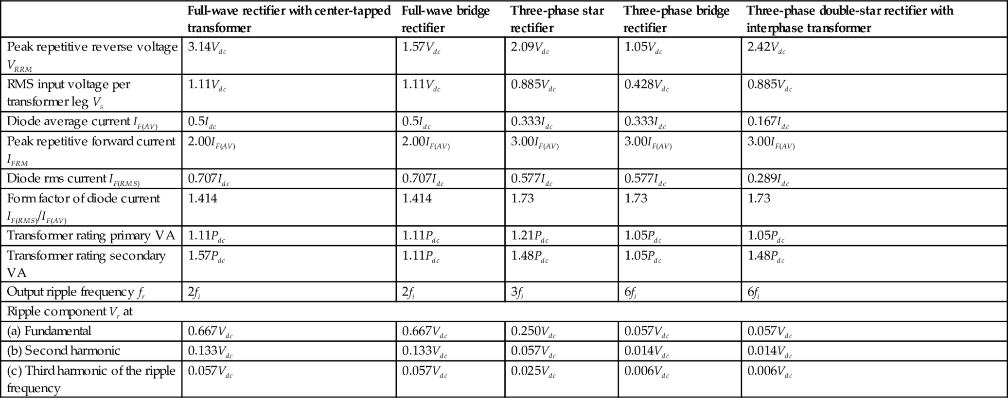
The important design parameters of typical single-phase and three-phase rectifiers with inductor-input dc filter are listed in Table 7.5. Note that, in a single-phase half-wave rectifier, a freewheeling diode is required to be connected across the input of the dc filters such that the flow of load current can be maintained during the negative half cycle of the supply voltage.
Table 7.5
Important design parameters of typical rectifier circuits with inductor-input dc filter
| Full-wave rectifier with center-tapped transformer | Full-wave bridge rectifier | Three-phase star rectifier | Three-phase bridge rectifier | Three-phase double-star rectifier with interphase transformer | |
| Peak repetitive reverse voltage VRRM | 3.14Vdc | 1.57Vdc | 2.09Vdc | 1.05Vdc | 2.42Vdc |
| RMS input voltage per transformer leg Vs | 1.11Vdc | 1.11Vdc | 0.885Vdc | 0.428Vdc | 0.885Vdc |
| Diode average current IF(AV) | 0.5Idc | 0.5Idc | 0.333Idc | 0.333Idc | 0.167Idc |
| Peak repetitive forward current IFRM | 2.00IF(AV) | 2.00IF(AV) | 3.00IF(AV) | 3.00IF(AV) | 3.00IF(AV) |
| Diode rms current IF(RMS) | 0.707Idc | 0.707Idc | 0.577Idc | 0.577Idc | 0.289Idc |
| Form factor of diode current IF(RMS)/IF(AV) | 1.414 | 1.414 | 1.73 | 1.73 | 1.73 |
| Transformer rating primary VA | 1.11Pdc | 1.11Pdc | 1.21Pdc | 1.05Pdc | 1.05Pdc |
| Transformer rating secondary VA | 1.57Pdc | 1.11Pdc | 1.48Pdc | 1.05Pdc | 1.48Pdc |
| Output ripple frequency fr | 2fi | 2fi | 3fi | 6fi | 6fi |
| Ripple component Vr at | |||||
| (a) Fundamental | 0.667Vdc | 0.667Vdc | 0.250Vdc | 0.057Vdc | 0.057Vdc |
| (b) Second harmonic | 0.133Vdc | 0.133Vdc | 0.057Vdc | 0.014Vdc | 0.014Vdc |
| (c) Third harmonic of the ripple frequency | 0.057Vdc | 0.057Vdc | 0.025Vdc | 0.006Vdc | 0.006Vdc |
7.5.2 Capacitive-Input DC Filters
Fig. 7.26 shows a full-wave rectifier with capacitor-input dc filter. The voltage and current waveforms of this rectifier are shown in Fig. 7.27. When the instantaneous voltage of the secondary winding vs is higher than the instantaneous value of capacitor voltage vL, either D1 or D2 conducts, and the capacitor C is charged up from the transformer. When the instantaneous voltage of the secondary winding vs falls below the instantaneous value of capacitor voltage vL, both the diodes are reverse biased and the capacitor C is discharged through load resistance R. The resulting capacitor voltage vL varies between a maximum value of Vm and a minimum value of Vm−Vr(pp)![]() as shown in Fig. 7.27. (Vr(pp) is the peak-to-peak ripple voltage.) As shown in Fig. 7.27, the conduction angle θc of the diodes becomes smaller when the output ripple voltage decreases. Consequently, the power supply and the diodes suffer from high repetitive surge currents. An LC ac filter, as shown in Fig. 7.24, may be required to improve the input power factor of the rectifier.
as shown in Fig. 7.27. (Vr(pp) is the peak-to-peak ripple voltage.) As shown in Fig. 7.27, the conduction angle θc of the diodes becomes smaller when the output ripple voltage decreases. Consequently, the power supply and the diodes suffer from high repetitive surge currents. An LC ac filter, as shown in Fig. 7.24, may be required to improve the input power factor of the rectifier.

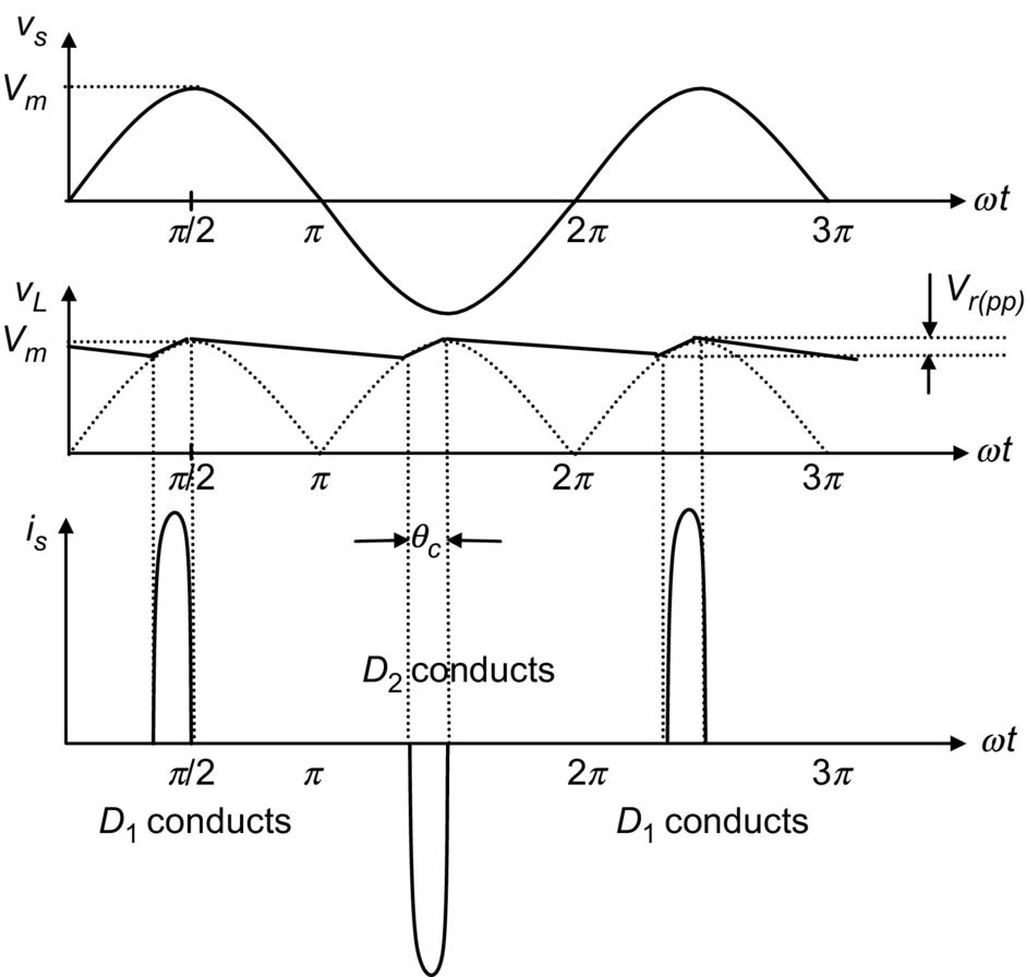
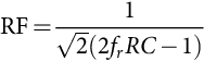
In practice, if the peak-to-peak ripple voltage is small, it can be approximated as
Vr(pp)=VmfrRC

where fr is the output ripple frequency of the rectifier.
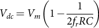
Therefore, the average output voltage Vdc is given by
Vdc=Vm(1−12frRC)
The rms output ripple voltage Vac is approximately given by
Vac=Vm2√2frRC
The ripple factor RF can be found from
RF=1√2(2frRC−1)
7.5.2.1 Inrush Current
The resistor Rinrush in Fig. 7.26 is used to limit the inrush current imposed on the diodes during the instant when the rectifier is being connected to the supply. The inrush current can be very large because capacitor C has zero charge initially. The worst case occurs when the rectifier is connected to the supply at its maximum voltage. The worst-case inrush current can be estimated from
Iinrush=VmRsec+RESR
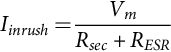
where Rsec is the equivalent resistance looking from the secondary transformer and RESR is the equivalent series resistance (ESR) of the filtering capacitor. Hence, the employed diode should be able to withstand the inrush current for a half cycle of the input voltage. In other words, the maximum allowable surge current (IFSM) rating of the employed diodes must be higher than the inrush current. The equivalent resistance associated with the transformer windings and the filtering capacitor is usually sufficient to limit the inrush current to an acceptable level. However, in cases where the transformer is omitted, for example, the rectifier of an off-line switch-mode supply, resistor Rinrush must be added for controlling the inrush current.
Consider as an example, a single-phase bridge rectifier, which is to be connected to a 120 V to 60 Hz source (without transformer). Assume that the IFSM rating of the diodes is 150 A for an interval of 8.3 ms. If the ESR of the filtering capacitor is zero, the value of the resistor for limiting inrush current resistance can be estimated to be 1.13 Ω using Eq. (7.81).
7.6 High-Frequency Diode Rectifier Circuits
In high-frequency converters, diodes perform various functions, such as rectifying, flywheeling, and clamping. One special quality a high-frequency diode must possess is a fast switching speed. In technical terms, it must have a short reverse recovery time and a short forward recovery time.
The reverse recovery time of a diode may be understood as the time a forwardly conducting diode takes to recover to a blocking state when the voltage across it is suddenly reversed (which is known as forced turnoff). The temporary short circuit during the reverse recovery period may result in large reverse current, excessive ringing, and large power dissipation, all of which are highly undesirable.
The forward recovery time of a diode may be understood as the time a nonconducting diode takes to change to the fully on state when a forward current is suddenly forced into it (which is known as forced turn-on). Before the diode reaches the fully on state, the forward voltage drop during the forward recovery time can be significantly higher than the normal on-state voltage drop. This may cause voltage spikes in the circuit.
It should be interesting to note that, as far as circuit operation is concerned, a diode with a long reverse recovery time is similar to a diode with a large parasitic capacitance. A diode with a long forward recovery time is similar to a diode with a large parasitic inductance. (Spikes caused by the slow forward recovery of diodes are often wrongly thought to be caused by leakage inductance.) Comparatively, the adverse effect of a long reverse recovery time is much worse than that of a long forward recovery time.
Among commonly used diodes, the Schottky diode has the shortest forward and reverse recovery times. Schottky diodes are therefore most suitable for high-frequency applications. However, Schottky diodes have relatively low reverse breakdown voltage (normally lower than 200 V) and large leakage current. If, due to these limitations, Schottky diodes cannot be used, ultrafast diodes should be used in high-frequency converter circuits.
Using the example of a forward converter, the operations of a forward rectifier diode, a flywheel diode, and a clamping diode will be studied in Section 7.6.1. Because of the difficulties encountered in the full analyses taking into account parasitic/stray/leakage components, PSpice simulations are extensively used here to study the following:
• The idealized operation of the converter
• The adverse effects of relatively slow rectifiers (e.g., the so-called ultrafast diodes, which are actually much slower than Schottky diodes)
• The improvement achievable by using high-speed rectifiers (Schottky diodes)
• The effects of leakage inductance of the transformer
• The use of snubber circuits to reduce ringing
• The operation of a practical converter with snubber circuits
Using the example of a flyback converter, the operations of a flyback rectifier diode and a clamping diode will also be studied in Section 7.6.2.
The design considerations for high-frequency diode rectifier circuits will be discussed in Section 7.6.3. Some precautions that must be taken in the interpretation of computer simulation results are briefed in Section 7.6.4.
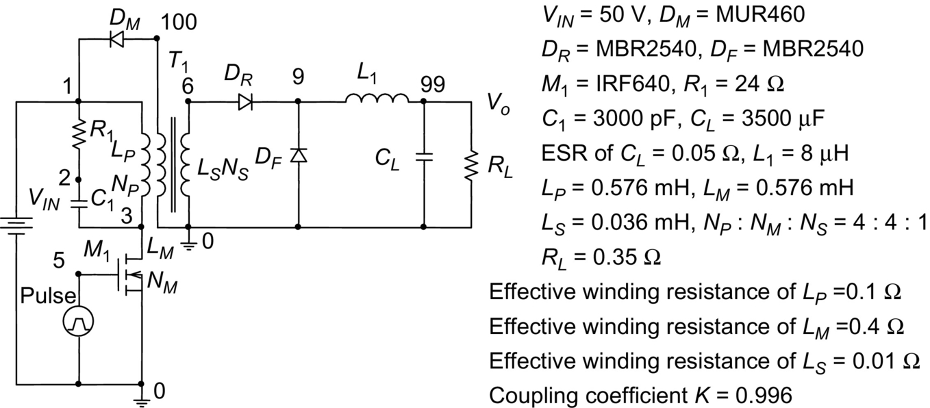
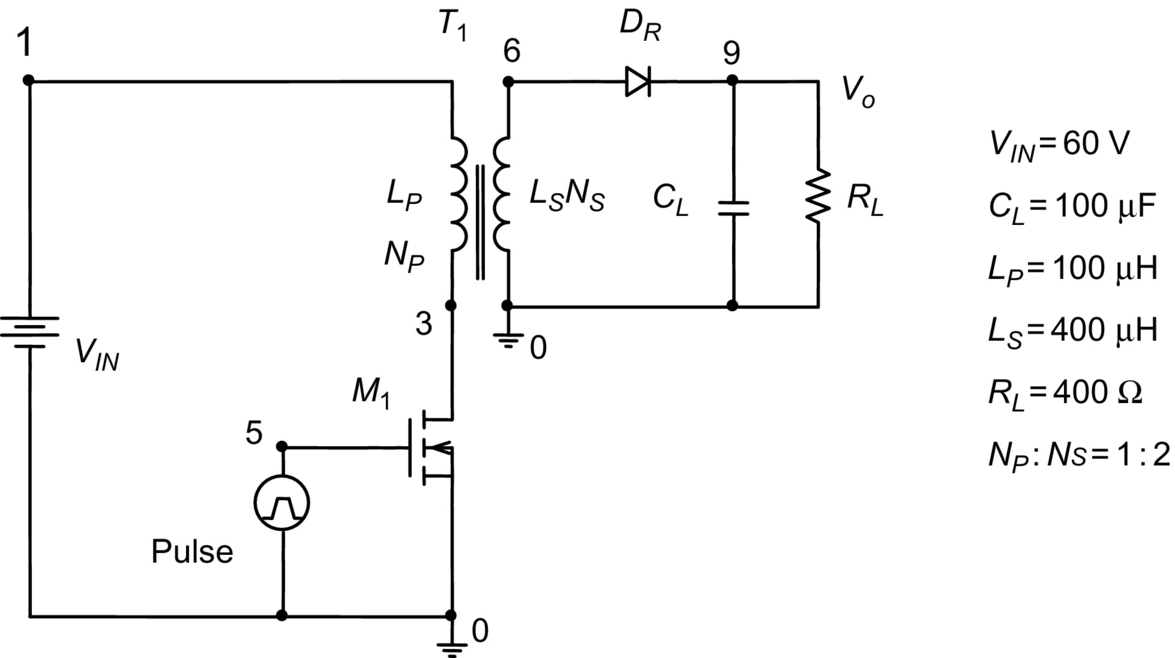
7.6.1 Forward Rectifier Diode, Flywheel Diode, and Magnetic-Reset Clamping Diode in a Forward Converter
7.6.1.1 Ideal Circuit
Fig. 7.28 shows the basic circuit of a forward converter. Fig. 7.29 shows the idealized steady-state waveforms for continuous-mode operation (the current in L1 being continuous). These waveforms are obtained from PSpice simulations, based on the following assumptions:
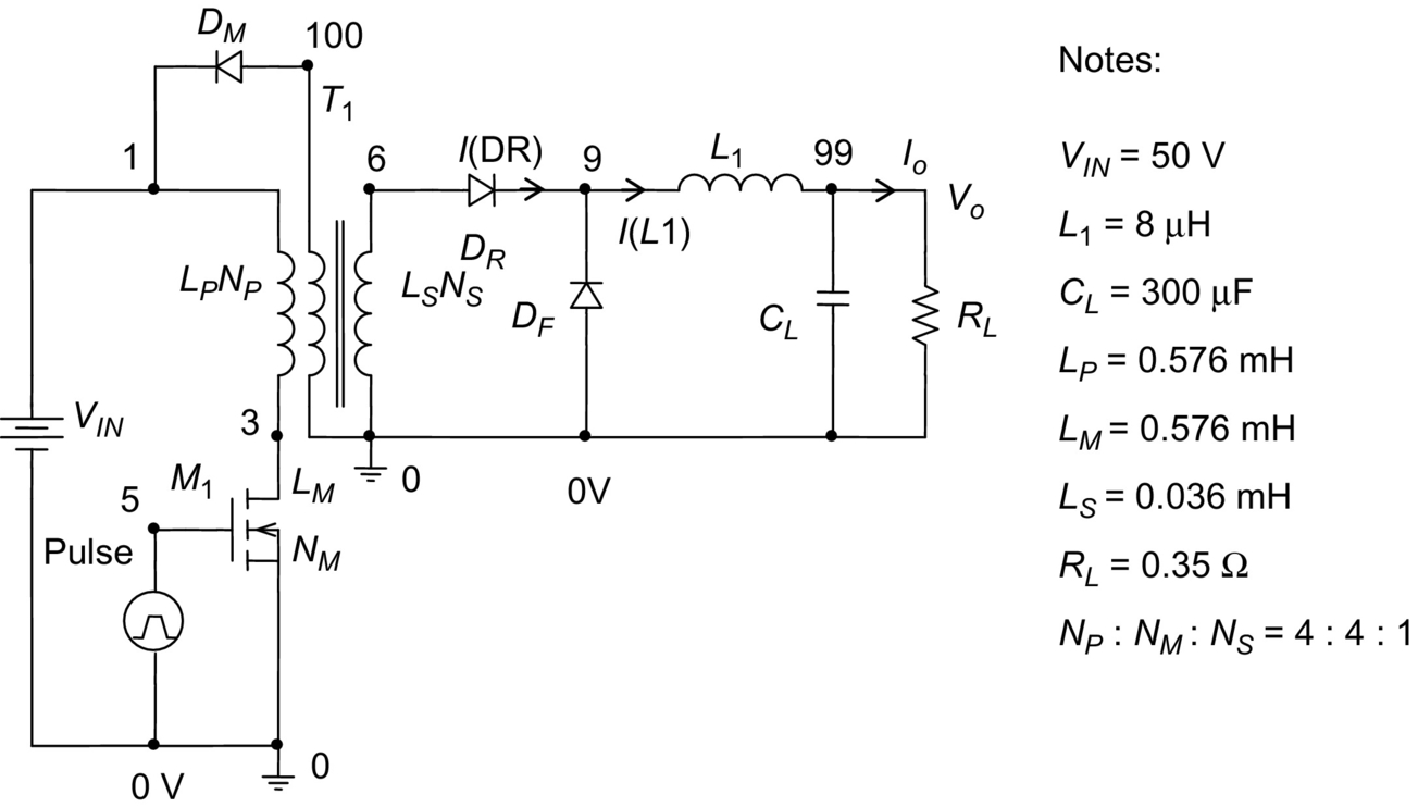
• Rectifier diode DR, flywheel diode DF, and magnetic-reset clamping diode DM are ideal diodes with infinitely fast switching speed.
• Electronic switch M1 is an idealized MOS switch with infinitely fast switching speed and
On-stateresistance=0.067ΩOff-stateresistance=1MΩ
It should be noted that PSpice does not allow a switch to have zero on-state resistance and infinite off-state resistance.
• Transformer T1 has a coupling coefficient of 0.99999999. PSpice does not accept a coupling coefficient of 1.
• The switching operation of the converter has reached a steady state.
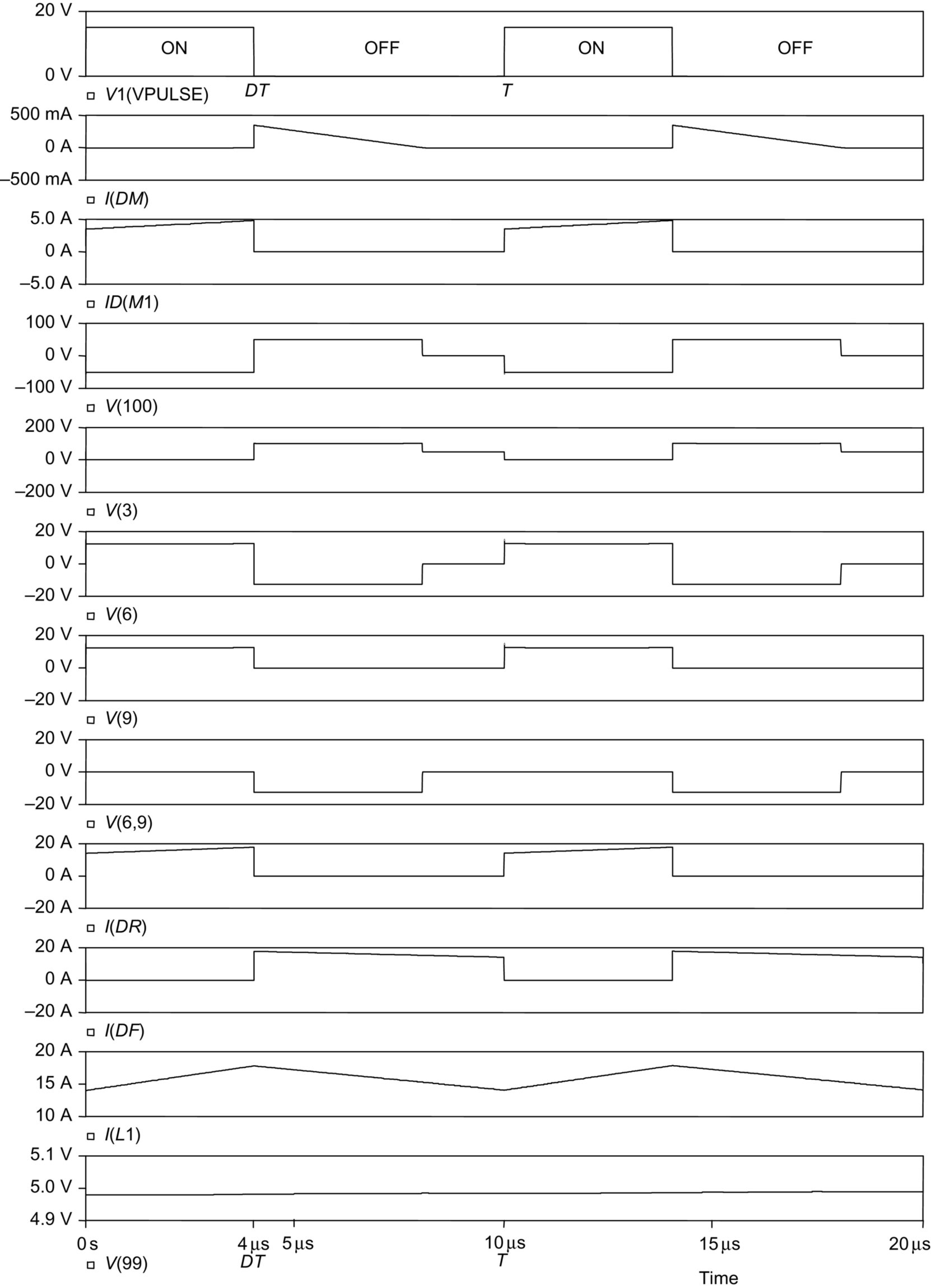
Referring to the circuit shown in Fig. 7.28 and the waveforms shown in Fig. 7.29, the operation of the converter can be explained as follows:
1. For 0<t<DT![]() (D is the duty cycle of the MOS switch M1 and T is the switching period of the converter. M1 is turned on when V1 (VPULSE) is 15 V and turned off when V1(VPULSE) is 0 V).
(D is the duty cycle of the MOS switch M1 and T is the switching period of the converter. M1 is turned on when V1 (VPULSE) is 15 V and turned off when V1(VPULSE) is 0 V).
The switch M1 is turned on at t=0![]() .
.
The voltage at node 3, denoted as V(3), is
V(3)=0for0<t<DT
The voltage induced at node 6 of the secondary winding LS is
V(6)=VIN(Ns/Np)
This voltage drives a current I(DR) (current through rectifier diode DR) into the output circuit to produce the output voltage Vo. The rate of increase of I(DR) is given by
dI(DR)dt=[VINNSNP−Vo]1L1
where Vo is the dc output voltage of the converter.
The flywheel diode DF is reversely biased by V(9), the voltage at node 9:
V(9)=VIN(NS/NP)for0<t<DT
The magnetic-reset clamping diode DM is reversely biased by the negative voltage at node 100. Assuming that LM and LP have the same number of turns, we have
V(100)=−VINfor0<t<DT
A magnetizing current builds up linearly in LP. This magnetizing current reaches the maximum value of (VINDT)/LP at t=DT![]() .
.
2. For DT<t<2DT![]()
The switch M1 is turned off at t=DT![]() .
.
The collapse of magnetic flux induces a back emf in LM, which is equal to LP, to turn-on the clamping diode DM. The magnetizing current in LM drops (from the maximum value of (VIN DT)/LP, as mentioned above) at the rate of VIN/LP. It reaches zero at t=2DT![]() .
.
The back emf induced across LP is equal to VIN. The voltage at node 3 is
V(3)=2VINforDT<t<2DT
The back emf across LS forces DR to stop conducting.
The inductive current in L1 forces the flywheel diode DF to conduct. I(L1) (current through L1) falls at the rate of
dI(L1)dt=−VoL1

The voltage across DR, denoted as V(6,9) (the voltage at node 6 with respect to node 9), is
V(DR)=V(6,9)=−VIN(NS/NP)forDT<t<2DT
3. For 2DT<t<T![]()
DM stops conducting at t=2DT![]() . The voltage across LM then falls to zero.
. The voltage across LM then falls to zero.
The voltage across LP is zero:
V(3)=VIN
The voltage across LS is also zero:
V(6)=0
Inductive current I(L1) continues to fall at the rate of
dI(L1)dt=−VoL1
The switching cycle restarts when the switch M1 is turned on again at t=T![]() .
.
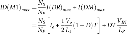
From the waveforms shown in Fig. 7.29, the following useful information (for continuous-mode operation) can be found:
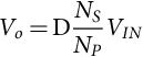
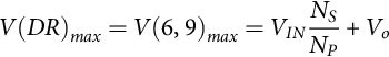
• The output voltage Vo is equal to the average value of V(9):
Vo=DNSNPVIN
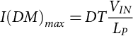
• The maximum current in the forward rectifying diode DR and flywheel diode DF is
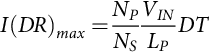
I(DR)max=I(DF)max=Io+12VoL1(1−D)T
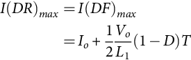
where Vo=DVIN(NS/NP)![]() and Io is the output loading current.
and Io is the output loading current.
• The maximum reverse voltage of DR and DF is
V(DR)max=V(DF)max=V(6,9)max=VINNSNP

• The maximum reverse voltage of DM is
V(DM)max=VIN
• The maximum current in DM is
I(DM)max=DTVINLP
• The maximum current in the switch M1, denoted as ID(M1), is
ID(M1)max=NSNPI(DR)max+I(DM)max=NSNP[Io+12VoL1(1−D)T]+DTVINLP
It should, however, be understood that, due to the nonideal characteristics of practical components, the idealized waveforms shown in Fig. 7.29 cannot actually be achieved in the real world. In the following, the effects of nonideal diodes and transformers will be examined.
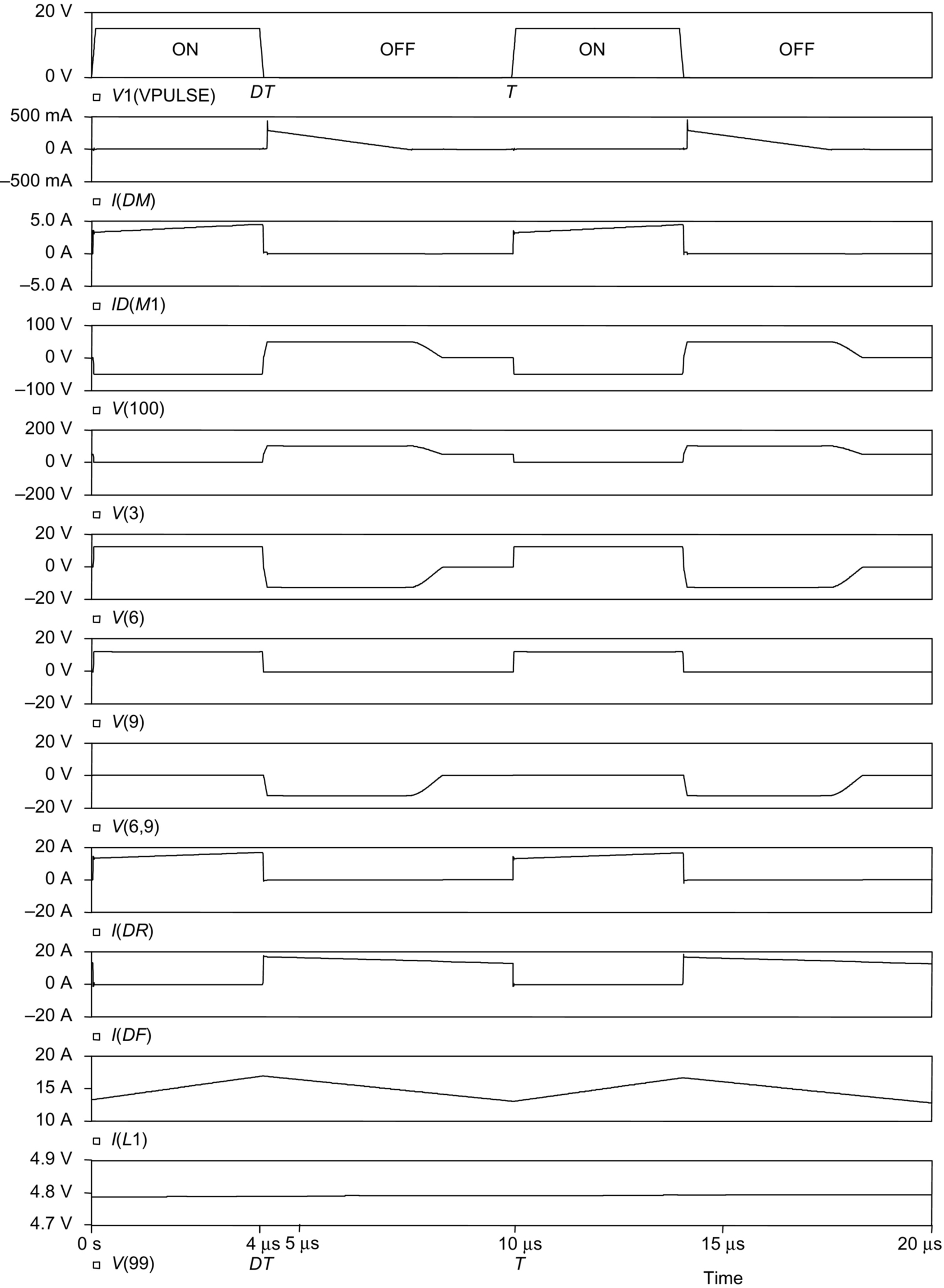
7.6.1.2 Circuit Using Ultra-Fast Diodes
Fig. 7.30 shows the waveforms of the forward converter (circuit given in Fig. 7.28) when ultrafast diodes are used as DM, DR, and DF. (Note that ultrafast diodes are actually much slower than Schottky diodes.) The waveforms are obtained by PSpice simulations, based on the following assumptions:
• DM is an MUR460 ultrafast diode. DR and DF are MUR1560 ultrafast diodes.
• M1 is an IRF640 MOS transistor.
• Transformer T1 has a coupling coefficient of 0.99999999 (which may be assumed to be 1).
• The switching operation of the converter has reached a steady state.
It is observed that a large spike appears in the current waveforms of diodes DR and DF (denoted as I(DR) and I(DF) in Fig. 7.30) whenever the MOS transistor M1 is turned on. This is due to the relatively slow reverse recovery of the flywheel diode DF. During the reverse recovery time, the positive voltage suddenly appearing across L S (which is equal to VIN (NS/NP)) drives a large transient current through DR and DF. This current spike results in large current stress and power dissipation in DR, DF, and M1.
A method of reducing the current spikes is to use Schottky diodes as DR and DF, as described below.
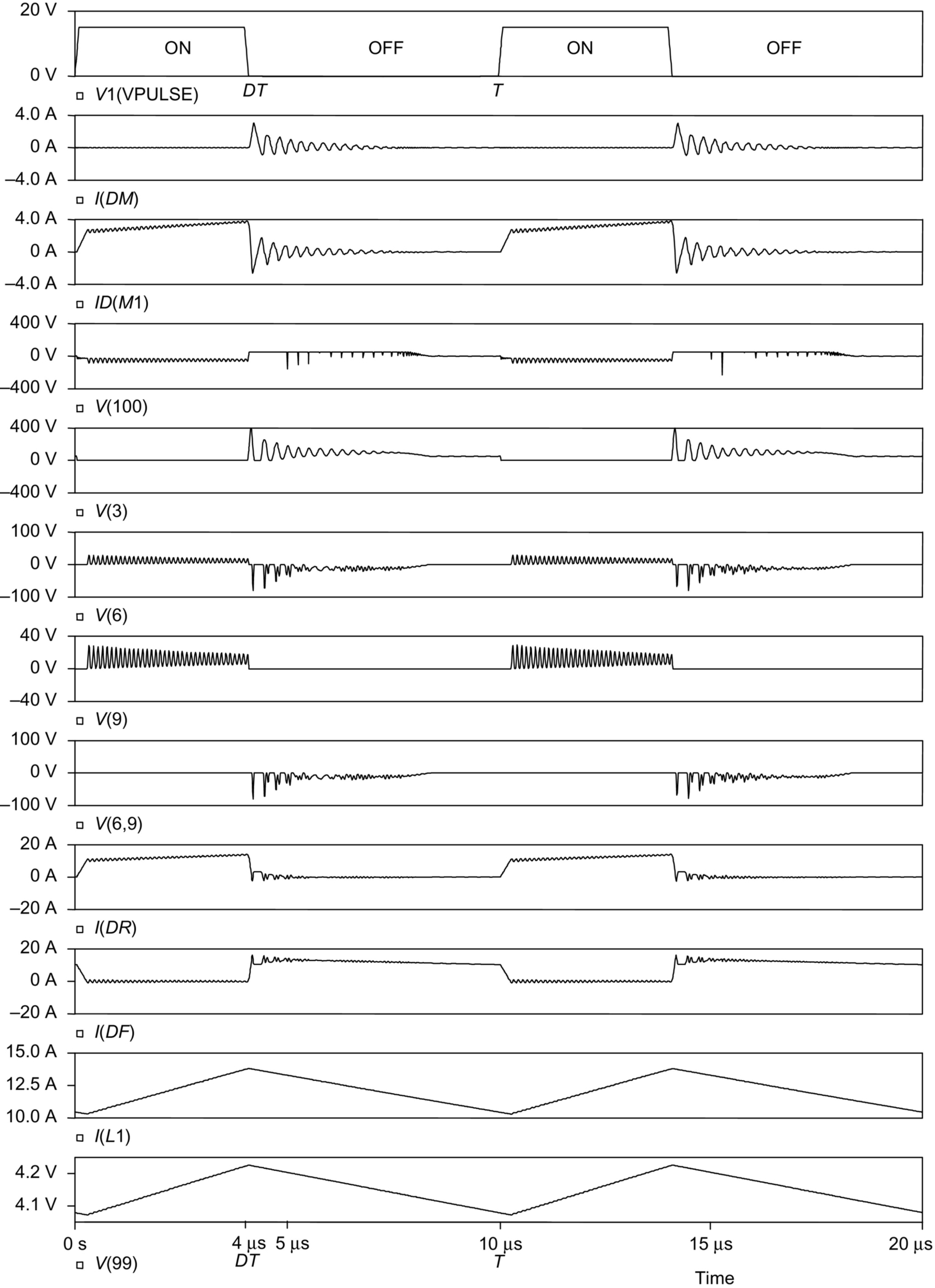
7.6.1.3 Circuit Using Schottky Diodes
In order to reduce the current spikes caused by the slow reverse recovery of rectifiers, Schottky diodes are now used as DR and DF. The assumptions made here are (referring to the circuit shown in Fig. 7.28) the following:
• DR and DF are MBR2540 Schottky diodes.
• DM is an MUR460 ultrafast diode.
• M1 is an IRF640 MOS transistor.
• Transformer T1 has a coupling coefficient of 0.99999999.
• The switching operation of the converter has reached a steady state.
The new simulated waveforms are given in Fig. 7.31. It is found that, by employing Schottky diodes as DR and DF, the amplitudes of the current spikes in ID(M1), I(DR), and I(DF) can be reduced to practically zero. This solves the slow-speed problem of ultrafast diodes.
7.6.1.4 Circuit With Practical Transformer
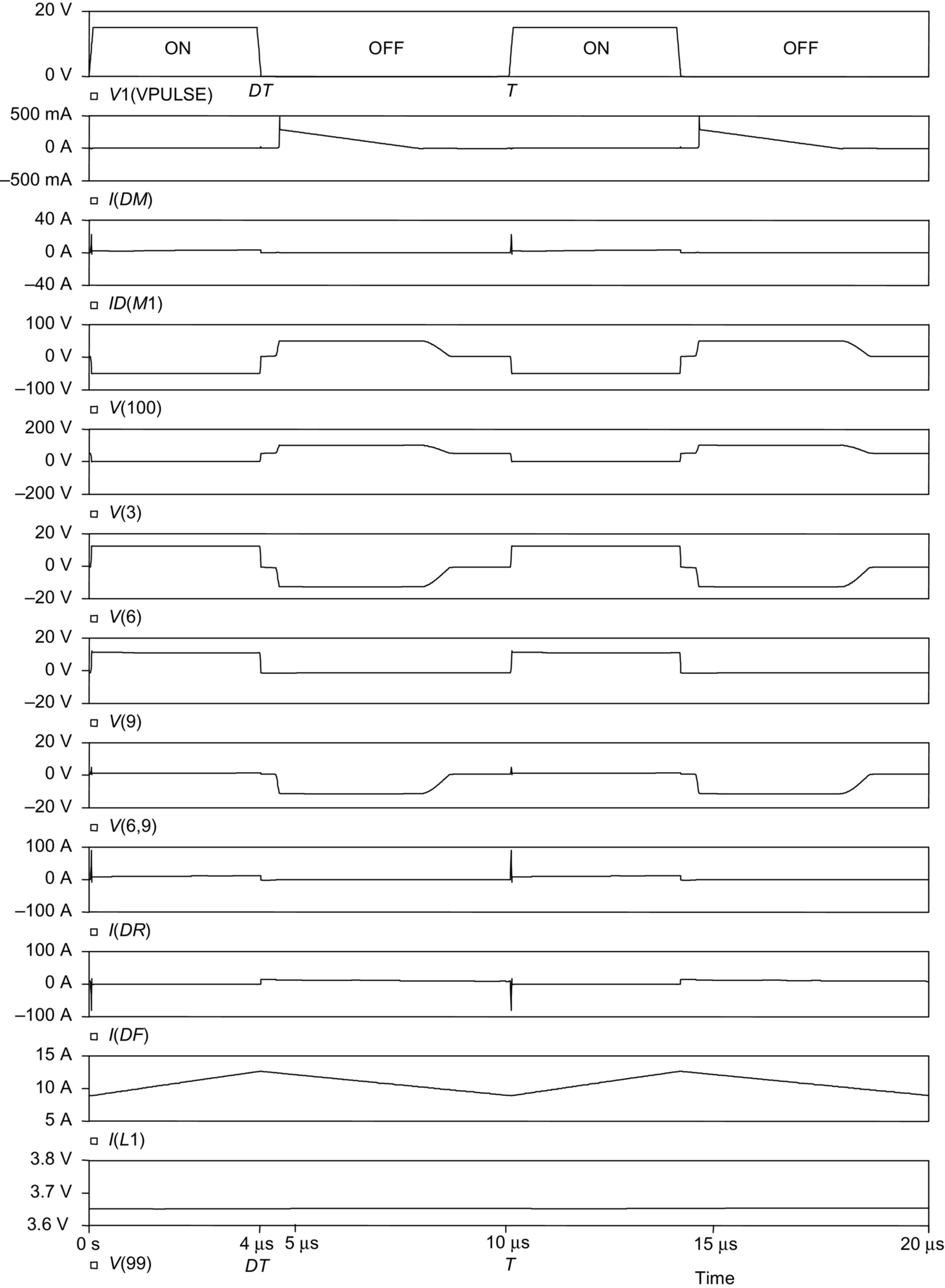
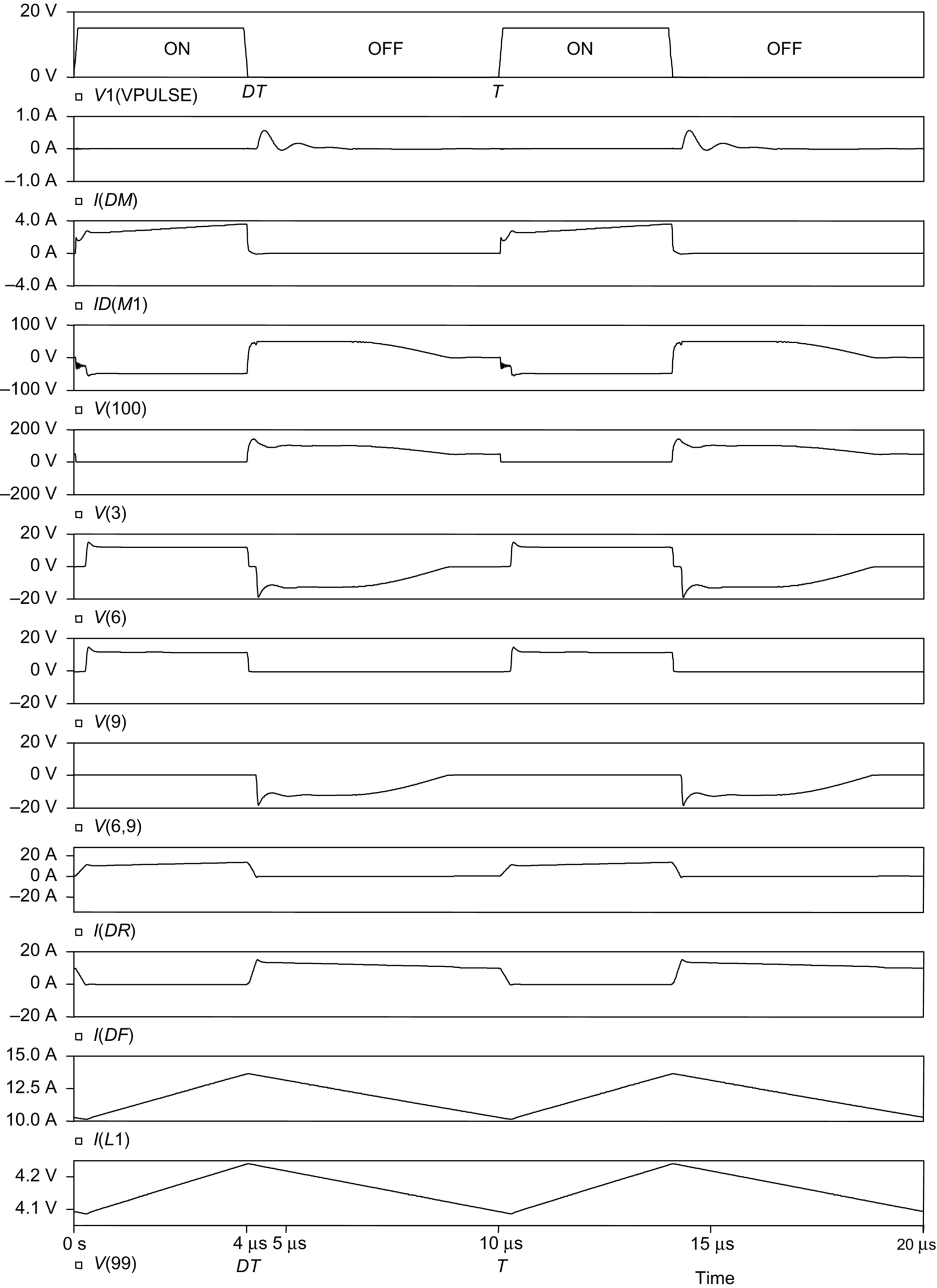
The simulation results given above in Figs. 7.29–7.31 (for the forward converter circuit shown in Fig. 7.28) are based on the assumption that transformer T1 has effectively no leakage inductance (with coupling coefficient K=0.99999999![]() ). It is, however, found that when a practical transformer (having a slightly lower K) is used, severe ringings occur. Fig. 7.32 shows some simulation results to demonstrate this phenomenon, where the following assumptions are made:
). It is, however, found that when a practical transformer (having a slightly lower K) is used, severe ringings occur. Fig. 7.32 shows some simulation results to demonstrate this phenomenon, where the following assumptions are made:
• DR and DF are MBR2540 Schottky diodes. DM is an MUR460 ultrafast diode.
• M1 is an IRF640 MOS transistor.
• Transformer T1 has a practical coupling coefficient of 0.996.
• The effective winding resistance of LP is 0.1 Ω. The effective winding resistance of LM is 0.4 Ω. The effective winding resistance of LS is 0.01 Ω.
• The effective series resistance of the output filtering capacitor is 0.05 Ω.
• The switching operation of the converter has reached a steady state.
The resultant waveforms shown in Fig. 7.32 indicate that there are large voltage and current ringings in the circuit. These ringings are caused by the resonant circuits formed by the leakage inductance of the transformer and the parasitic capacitances of diodes and transistor.
A practical converter may therefore need snubber circuits to damp these ringings, as described below.
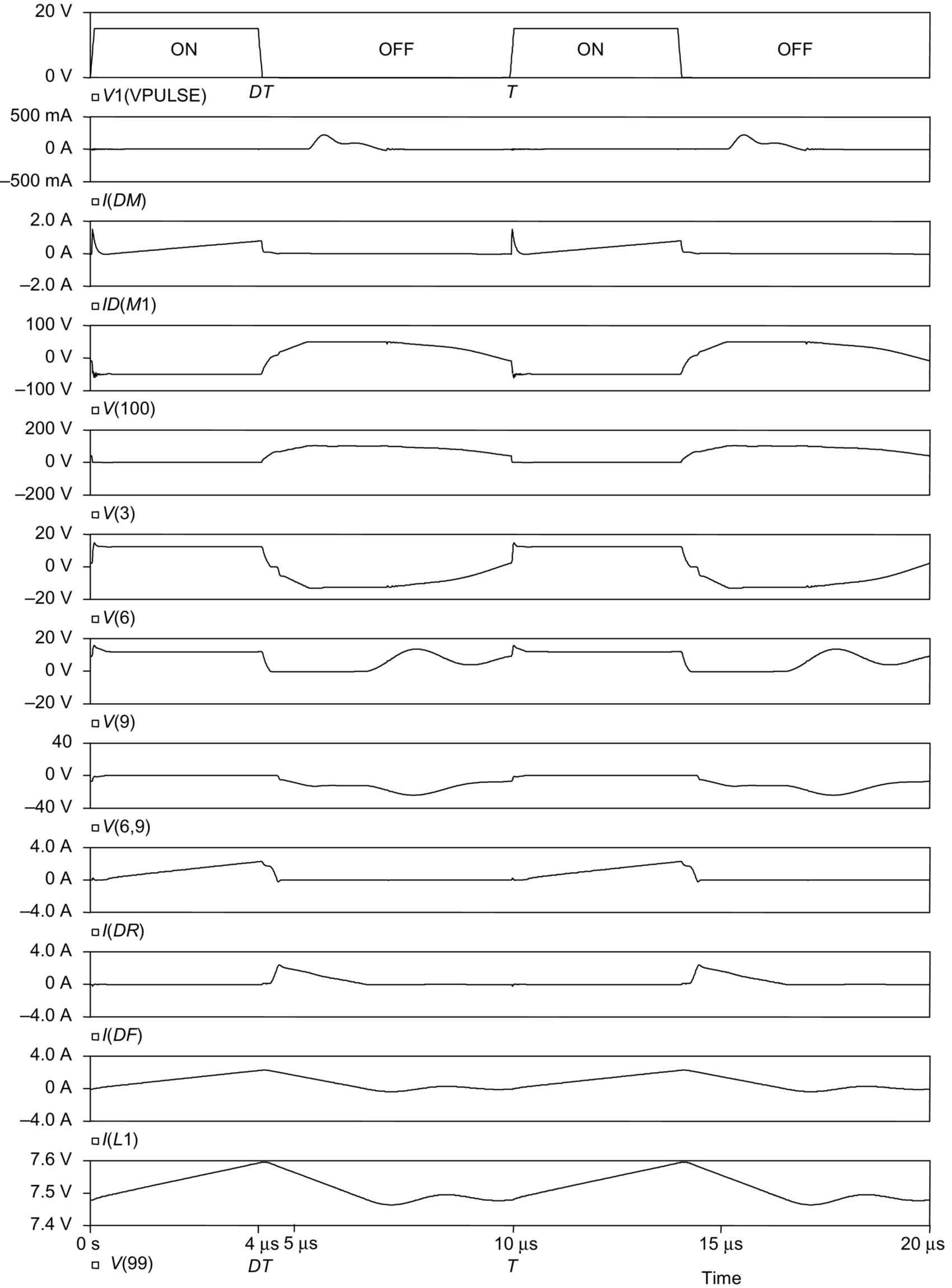
7.6.1.5 Circuit With Snubber Across The Transformer
In order to suppress the ringing voltage caused by the resonant circuit formed by transformer leakage inductance and the parasitic capacitance of the MOS switch, a snubber circuit, shown as R1 and C1 in Fig. 7.33, is now connected across the primary winding of transformer T1. The new waveforms are shown in Fig. 7.34. Here, the drain-to-source voltage waveform of the MOS transistor, V(3), is found to be acceptable. However, there are still large ringing voltages across the output rectifiers (V(6,9) and V(9)).

In order to damp the ringing voltages across the output rectifiers, additional snubber circuits across the rectifiers may therefore also be required in a practical circuit, as described below.
7.6.1.6 Practical Circuit
Fig. 7.35 shows a practical forward converter with snubber circuits added also to rectifiers (R2C2 for DR and R3C3 for DF) to reduce the voltage ringing. Figs. 7.36 and 7.37 show the resultant voltage and current waveforms. Fig. 7.36 is for continuous-mode operation (RL=0.35Ω)![]() , where I(L1) (current in L1) is continuous. Fig. 7.37 is for discontinuous-mode operation (RL=10Ω)
, where I(L1) (current in L1) is continuous. Fig. 7.37 is for discontinuous-mode operation (RL=10Ω)![]() , where I(L1) becomes discontinuous due to an increased value of RL. These waveforms are considered to be acceptable.
, where I(L1) becomes discontinuous due to an increased value of RL. These waveforms are considered to be acceptable.

The design considerations of diode rectifier circuits in high-frequency converters will be discussed later in Section 7.6.3.
7.6.2 Flyback Rectifier Diode and Clamping Diode in a Flyback Converter
7.6.2.1 Ideal Circuit
Fig. 7.38 shows the basic circuit of a flyback converter. Due to its simple circuit, this type of converter is widely used in low-cost low-power applications. Discontinuous-mode operation (meaning that the magnetizing current in the transformer falls to zero before the end of each switching cycle) is often used because it offers the advantages of easy control and low diode reverse recovery loss. Fig. 7.39 shows the idealized steady-state waveforms for discontinuous-mode operation. These waveforms are obtained from PSpice simulations, based on the following assumptions:
• DR is an idealized rectifier diode with infinitely fast switching speed.
• M1 is an idealized MOS switch with infinitely fast switching speed and
On-stateresistance=0.067ΩOff-stateresistance=1MΩ
• Transformer T1 has a coupling coefficient of 0.99999999.
• The switching operation of the converter has reached a steady state.
Referring to the circuit shown in Fig. 7.38 and the waveforms shown in Fig. 7.39, the operation of the converter can be explained as follows:
1. For 0<t<DT![]()
The switch M1 is turned on at t=0![]() :
:
V(3)=0for0<t<DT
The current in M1, denoted as ID(M1), increases at the rate of
dID(M1)dt=VINLP

The output rectifier DR is reversely biased.
2. For DT<t<(D+D2)T![]()
The switching M1 is turned off at t=DT![]() .
.
The collapse of magnetic flux induces a back emf in LS to turn-on the output rectifier DR. The initial amplitude of the rectifier current I(DR), which is also denoted as I(LS), can be found by equating the energy stored in the primary winding current I(LP) just before t=DT![]() to the energy stored in the secondary winding current I(LS) just after t=DT
to the energy stored in the secondary winding current I(LS) just after t=DT![]() :
:
12LP[I(LP)]2=12LS[I(LS)]2
12LP[VINLPDT]2=12LS[I(LS)]2

I(LS)=√LPLSVINLPDT
I(LS)=NPNSVINLPDT
The amplitude of I(LS) falls at the rate of
dI(LS)dt=−VoLS

and I(LS) falls to zero at t=(D+D2)T. Since D2Vo=VIN(NS/NP)D![]() ,
,
D2=VINVoNSNPD
D2 is effectively the duty cycle of the output rectifier DR.
3. For (D+D2)T<t<T![]()
The output rectifier DR is off.
The output capacitor CL provides the output current to the load RL.
The switching cycle restarts when the switch M1 is turned on again at t=T![]() .
.
From the waveforms shown in Fig. 7.39, the following information (for discontinuous-mode operation) can be obtained:
• The maximum value of the current in the switch M1 is
ID(M1)max=VINLPDT
• The maximum value of the current in the output rectifier DR is
I(DR)max=NPNSVINLPDT
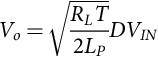
• The output voltage Vo can be found by equating the input energy to the output energy within a switching cycle.
VIN×[ChargetakenfromVINinaswitchingcycle]=V2oRLT

VIN[12DTDTLPVIN]=V2oRLT
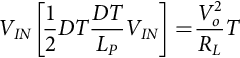
Vo=√RLT2LPDVIN
• The maximum reverse voltage of DR, V(6,9) (which is the voltage at node 6 with respect to node 9), is
V(DR)max=V(6,9)max=VINNSNP+Vo
7.6.2.2 Practical Circuit
When a practical transformer (with leakage inductance) is used in the flyback converter circuit shown in Fig. 7.38, there will be large ringings. In order to reduce these ringings to practically acceptable levels, snubber and clamping circuits have to be added. Fig. 7.40 shows a practical flyback converter circuit where a resistor-capacitor snubber (R2C2) is used to damp the ringing voltage across the output rectifier DR and a resistor-capacitor-diode clamping (R1C1DS) is used to clamp the ringing voltage across the switch M1. What the diode DS does here is to allow the energy stored by the current in the leakage inductance to be converted to the form of a dc voltage across the clamping capacitor C1. The energy transferred to C1 is then dissipated slowly in the parallel resistor R1, without ringing problems.
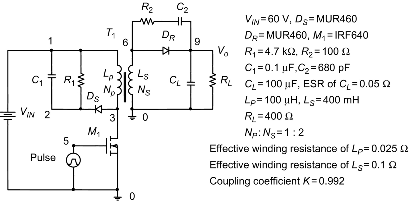
The simulated waveforms of the flyback converter (circuit given in Fig. 7.40) for discontinuous-mode operation are shown in Fig. 7.41, where the following assumptions are made:

• DR and DS are MUR460 ultrafast diodes.
• M1 is an IRF640 MOS transistor.
• Transformer T1 has a practical coupling coefficient of 0.992.
• The effective winding resistance of LP is 0.025 Ω. The effective winding resistance of LS is 0.1 Ω.
• The effective series resistance of the output filtering capacitor CL is 0.05 Ω.
• The switching operation of the converter has reached a steady state.
The waveforms shown in Fig. 7.40 are considered to be acceptable.
7.6.3 Design Considerations
In the design of rectifier circuits, it is necessary for the designer to determine the voltage and current ratings of the diodes. The idealized waveforms and expressions for the maximum diode voltages and currents given under the heading of “Ideal Circuit” above (for both forward and flyback converters) are a good starting point. However, when parasitic/stray components are also considered, the simulation results given under “Practical Circuit” are much more useful for the determination of the voltage and current ratings of the high-frequency rectifier diodes.
Assuming that the voltage and current ratings have been determined, proper diodes can be selected to meet the requirements. The following are some general guidelines on the selection of diodes:
• For low-voltage applications, Schottky diodes should be used because they have very fast switching speed and low forward voltage drop. If Schottky diodes cannot be used, either because of their low reverse breakdown voltage or because of their large leakage current (when reversely biased), ultrafast diodes should be used.
• The reverse breakdown voltage rating of the diode should be reasonably higher (e.g., 10% or 20% higher) than the maximum reverse voltage, the diode is expected to encounter under the worst-case condition. However, an overly conservative design (using a diode with much higher breakdown voltage than necessary) would result in a lower rectifier efficiency, because a diode having a higher reverse voltage rating would normally have a larger voltage drop when it is conducting.
• The current rating of the diode should be substantially higher than the maximum current the diode is expected to carry during normal operation. Using a diode with a relatively large current rating has the following advantages:
• It reduces the possibility of damage due to transients caused by start-up, accidental short circuit, or random turning on and off of the converter.
• It reduces the forward voltage drop because the diode is operated in the lower current region of the V-I characteristic.
In some of the “high-efficiency” converter circuits, the current rating of the output rectifier can be many times larger than the actual current expected in the rectifier. In this way, a higher efficiency is achieved at the expense of a larger silicon area.
In the design of R-C snubber circuits for rectifiers, it should be understood that a larger C (and a smaller R) will give better damping. However, a large C (and a small R) will result in a large switching loss (which is equal to 0.5 CV2f). As a guideline, a capacitor with five to ten times the junction capacitance of the rectifier may be used as a starting point for iterations. The value of the resistor should be chosen to provide a slightly underdamped operating condition.
7.6.4 Precautions in Interpreting Simulation Results
In using the simulated waveforms as references for design purposes, attention should be paid to the following:
• The voltage/current spikes that appear in the practically measured waveforms may not appear in the simulated waveforms. This is due to the lack of a model in the computer simulation to simulate unwanted coupling among the practical components.
• Most of the computer models of diodes, including those used in the simulations given above, do not take into account the effects of the forward recovery time. (The forward recovery time is not even mentioned in most manufacturers' data sheets.) However, it is also interesting to note that in most cases, the effect of the forward recovery time of a diode is masked by that of the effective inductance in series with the diode (e.g., the leakage inductance of a transformer).