
Multilevel Power Converters
Leon M. Tolbert The University of Tennessee, Knoxville, TN, United States
Xiaojie Shi The University of Tennessee, Knoxville, TN, United States
Abstract
This chapter covers the fundamental multilevel converter structures and modulation paradigms. The basic principles of the four main different multilevel converters have been discussed methodically: (1) cascaded H-bridges, (2) diode clamp, (3) flying capacitors, and (4) modular multilevel converter. Various modulation schemes for multilevel converters are also covered including fundamental frequency switching and harmonic elimination and several carrier-based and space vector-based pulse-width modulation (PWM) methods. The chapter also includes significant content on the operation and control of modular multilevel converter (MMCs) including techniques to balance capacitor voltage and reduce circulating current in converter arms.
Keywords
Multilevel converter; Multilevel inverter; Cascaded H-bridges; Diode-clamped converter; Flying capacitor converter; Modular multilevel converter
13.1 Introduction
Numerous industrial applications require higher power apparatus in recent years. Some medium-voltage motor drives and utility applications require medium-voltage and megawatt power level converters. For a medium-voltage grid, it is troublesome to connect only one power semiconductor switch directly. Hence, a multilevel power converter structure has been introduced as an alternative in high-power and medium-voltage situations. A multilevel converter not only achieves high-power ratings but also enables the use of renewable energy sources. Renewable energy sources such as photovoltaics or wind turbines can be easily interfaced to a multilevel converter system for a high-power utility application [1–3].
The concept of multilevel converters has been introduced since 1975 [4]. The term multilevel began with the three-level converter [5]. Subsequently, several multilevel converter topologies have been developed [6–13]. However, the basic concept of a multilevel converter to achieve higher power is to use a series of power semiconductor switches with several lower voltage dc sources to perform the power conversion by synthesizing a staircase voltage waveform. Capacitors, batteries, and renewable energy voltage sources can be used as the multiple dc voltage sources. The commutation of the power switches aggregate these multiple dc sources to achieve high voltage at the output; however, the rated voltage of the power semiconductor switches depends only on the rating of the dc voltage sources to which they are connected.
A multilevel converter has several advantages over a conventional two-level converter that uses high switching frequency pulse-width modulation (PWM). The attractive features of a multilevel converter are summarized as follows:
• Staircase waveform quality: Multilevel converters not only can generate the output voltages with very low distortion but also can reduce the dv/dt stresses; therefore, electromagnetic compatibility (EMC) problems can be reduced.
• Common-mode (CM) voltage: Multilevel converters produce smaller CM voltage; therefore, the stress in the bearings of a motor connected to a multilevel motor drive can be reduced. Furthermore, CM voltage can be eliminated by using advanced modulation strategies such as that proposed in [14].
• Input current: Multilevel converters can draw input current with low distortion.
• Switching frequency: Multilevel converters can operate at both fundamental switching frequency and high switching frequency PWM. It should be noted that lower switching frequency usually means lower switching loss and higher efficiency.
Unfortunately, multilevel converters do have some disadvantages. One particular disadvantage is the requirement of greater number of power semiconductor switches. Although lower voltage rated switches can be utilized in a multilevel converter, each switch requires a related gate-drive circuit. This may cause the overall system to be more expensive and complex.
Many multilevel converter topologies have been proposed during the last two decades. Contemporary research has engaged novel converter topologies and unique modulation schemes. Moreover, four different major multilevel converter structures have been reported in the literature: cascaded H-bridge converter with separate dc sources, diode clamp (neutral-clamped), flying capacitors (capacitor-clamped), and modular multilevel converter. Moreover, abundant modulation techniques and control paradigms have been developed for multilevel converters, such as sinusoidal pulse-width modulation (SPWM), selective harmonic elimination (SHE PWM), and space vector modulation (SVM). In addition, many multilevel converter applications focus on industrial medium-voltage motor drives [11,15], utility interface for renewable energy systems [16], flexible ac transmission system (FACTS) [17], and traction drive systems [18].
This chapter reviews the state of the art of multilevel power converter technology. Fundamental multilevel converter structures and modulation paradigms are discussed including the pros and cons of each. The main focus is on modern and more practical industrial applications of multilevel converters. Finally, the possible future developments of multilevel converter technology are noted.
13.2 Multilevel Power Converter Structures
As mentioned earlier, four different major multilevel converter structures have been used in industrial applications: cascaded H-bridge converter with separate dc sources, diode clamped, flying capacitors, and modular multilevel converter. It should be noted that the term multilevel converter refers to a power electronic circuit that could operate in an inverter or rectifier mode. The multilevel inverter structures are the focus of this chapter; however, the illustrated structures can be implemented for rectifying operation as well.
13.2.1 Cascaded H-Bridges
A single-phase structure of an m-level cascaded inverter is illustrated in Fig. 13.1. Each separate dc source (SDCS) is connected to a single-phase full-bridge or H-bridge inverter.

Each inverter level can generate three different voltage outputs, ![]() , and
, and ![]() , by connecting the dc source to the ac output by different combinations of the four switches: S1, S2, S3, and S4. To obtain
, by connecting the dc source to the ac output by different combinations of the four switches: S1, S2, S3, and S4. To obtain ![]() , switches S1 and S4 are turned on, whereas to obtain
, switches S1 and S4 are turned on, whereas to obtain ![]() , switches S2 and S3 are turned on. By turning on either S1 and S2 or S3 and S4, the output voltage will be zero. The ac outputs of each of the different full-bridge inverter levels are connected in series such that the synthesized voltage waveform is the sum of the inverter outputs. The number of output phase voltage levels, m, in a cascade inverter is defined by
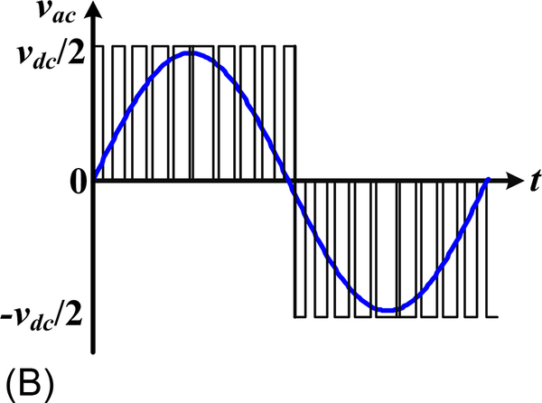
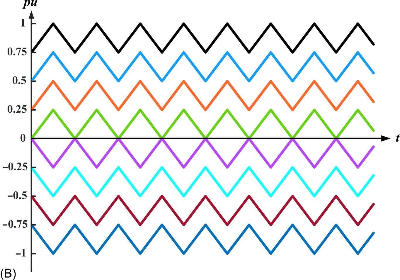
, switches S2 and S3 are turned on. By turning on either S1 and S2 or S3 and S4, the output voltage will be zero. The ac outputs of each of the different full-bridge inverter levels are connected in series such that the synthesized voltage waveform is the sum of the inverter outputs. The number of output phase voltage levels, m, in a cascade inverter is defined by ![]() , where s is the number of separate dc sources. An example of phase voltage waveform for an 11-level cascaded H-bridge inverter with five SDCSs and five full bridges is shown in Fig. 13.2. The phase voltage
, where s is the number of separate dc sources. An example of phase voltage waveform for an 11-level cascaded H-bridge inverter with five SDCSs and five full bridges is shown in Fig. 13.2. The phase voltage ![]() .
.
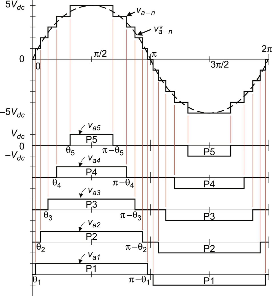
For a stepped waveform such as the one depicted in Fig. 13.2 with s steps, the Fourier transform for this waveform follows [14,18]:
From Eq. (13.1), the magnitudes of the Fourier coefficients when normalized with respect to Vdc are as follows:

The conducting angles, θ1,θ2,…,θs, can be chosen such that the voltage total harmonic distortion is minimum. Generally, these angles are chosen so that predominant lower frequency harmonics, 5, 7, 11, and 13 are eliminated [19]. More details on harmonic elimination techniques will be discussed in the following section.
Multilevel cascaded inverters have been proposed for such applications as static var generation, an interface with renewable energy sources, and for battery-based applications.
Three-phase cascaded inverters can be connected in wye, as shown in Fig. 13.3, or in delta. Peng et al. have demonstrated a prototype multilevel cascaded static var generator connected in parallel with an electric system that could supply or draw reactive current from an electric system [20–23]. The inverter could be controlled to regulate either the power factor of the current drawn from the source or the bus voltage of the electric system where the inverter was connected. Peng et al. [20] and Joos et al. [24] have also shown that a cascade inverter can be directly connected in series with the electric system for static var compensation. Cascaded inverters are ideal for connecting renewable energy sources with an ac grid because of the need for separate dc sources in applications such as photovoltaics or fuel cells.

Cascaded inverters have also been proposed for use as the main traction drive in electric vehicles where several batteries or ultracapacitors are well suited to serve as SDCSs [18,25]. The cascaded inverter could also serve as a rectifier or charger for the batteries of an electric vehicle while the vehicle was connected to an ac supply as shown in Fig. 13.3. In addition, the cascade inverter can act as a rectifier in a vehicle that uses regenerative braking.
Manjrekar and Lipo have proposed a cascade topology that uses multiple dc levels, which instead of being identical in value are multiples of each other [26,27]. They also used a combination of fundamental frequency switching for some of the levels and PWM switching for part of the levels to achieve the output voltage waveform. This approach enables a wider diversity of output voltage magnitudes; however, it also results in unequal voltage and current ratings for each of the levels and loses the advantage of being able to use identical modular units for each level.
The main advantages and disadvantages of multilevel cascaded H-bridge converters are as follows [28,29]:
13.2.1.1 Advantages
• The number of possible output voltage levels is more than twice the number of dc sources ![]() .
.
• The series of H-bridges makes for modularized layout and packaging. This will enable the manufacturing process to be done more quickly and cheaply.
13.2.1.2 Disadvantages
• Separate dc sources are required for each of the H-bridges. This will limit its application to products that already have multiple SDCSs readily available.
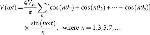
Another kind of cascaded multilevel converter with transformers using standard three-phase bilevel converters has been proposed [14]. The circuit is shown in Fig. 13.4. The converter uses output transformers to add different voltages. In order to add up the converter output voltages, the outputs of the three converters need to be synchronized with a separation of ![]() between each phase. For example, for obtaining a three-level voltage between outputs a and b, the output voltage can be synthesized by
between each phase. For example, for obtaining a three-level voltage between outputs a and b, the output voltage can be synthesized by ![]() . An isolated transformer is used to provide voltage boost. With three converters synchronized, the voltages,
. An isolated transformer is used to provide voltage boost. With three converters synchronized, the voltages, ![]() , are all in phase, and thus, the output level can be tripled [1].
, are all in phase, and thus, the output level can be tripled [1].
The advantage of the cascaded multilevel converters with transformers using standard three-phase bilevel converters is that the three converters are identical, and thus, control is more simple. However, the three converters need separate dc sources, and a transformer is needed to add up the output voltages.
13.2.2 Diode-Clamped Multilevel Inverter
The neutral point converter proposed by Nabae, Takahashi, and Akagi in 1981 was essentially a three-level diode-clamped inverter [5]. Several researchers published articles that have reported experimental results for four-, five-, and six-level diode-clamped converters for uses such as static var compensation, variable speed motor drives, and high-voltage system interconnections [17–30]. A three-phase six-level diode-clamped inverter is shown in Fig. 13.5. Each of the three phases of the inverter shares a common dc bus, which has been subdivided by five capacitors into six levels. The voltage across each capacitor is Vdc, and the voltage stress across each switching device is limited to Vdc through the clamping diodes. Table 13.1 lists the output voltage levels possible for one phase of the inverter with the negative dc rail voltage V0 as a reference. State condition 1 means the switch is on, and 0 means the switch is off. Each phase has five complementary switch pairs such that turning on one of the switches of the pair requires the other complementary switch to be turned off. The complementary switch pairs for phase-leg a are ![]() , and
, and ![]() . Table 13.1 also shows that in a diode-clamped inverter, the switches that are on for a particular phase leg are always adjacent and in series. For a six-level inverter, a set of five switches should be on at any given time.
. Table 13.1 also shows that in a diode-clamped inverter, the switches that are on for a particular phase leg are always adjacent and in series. For a six-level inverter, a set of five switches should be on at any given time.
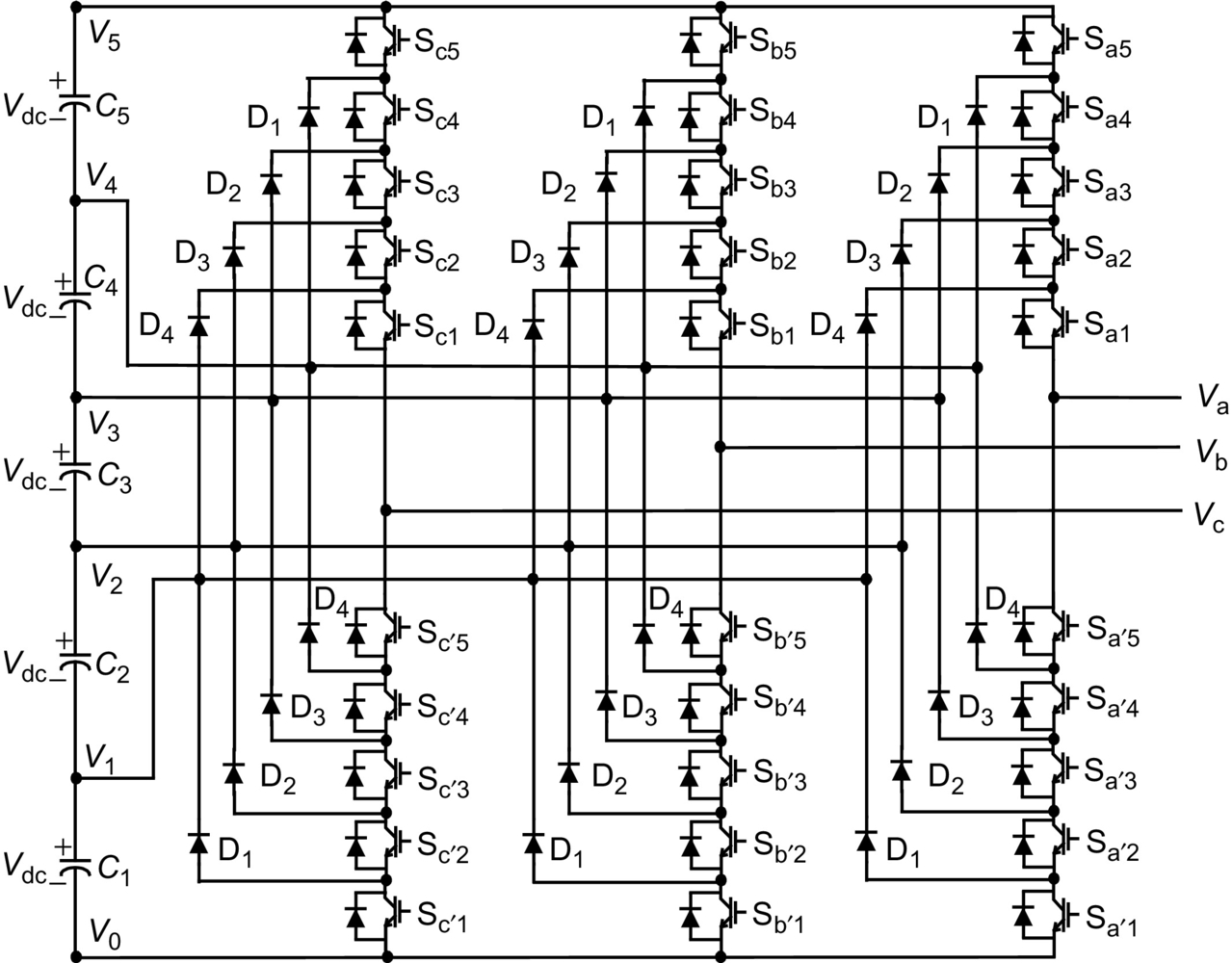
Table 13.1
Diode-clamped six-level inverter voltage levels and corresponding switch states
| Voltage Va0 | Switch state | |||||||||
| Sa5 | Sa4 | Sa3 | Sa2 | Sa1 | ||||||
| 1 | 1 | 1 | 1 | 1 | 0 | 0 | 0 | 0 | 0 | |
| 0 | 1 | 1 | 1 | 1 | 1 | 0 | 0 | 0 | 0 | |
| 0 | 0 | 1 | 1 | 1 | 1 | 1 | 0 | 0 | 0 | |
| 0 | 0 | 0 | 1 | 1 | 1 | 1 | 1 | 0 | 0 | |
| 0 | 0 | 0 | 0 | 1 | 1 | 1 | 1 | 1 | 0 | |
| 0 | 0 | 0 | 0 | 0 | 1 | 1 | 1 | 1 | 1 | |
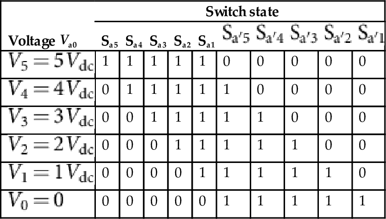
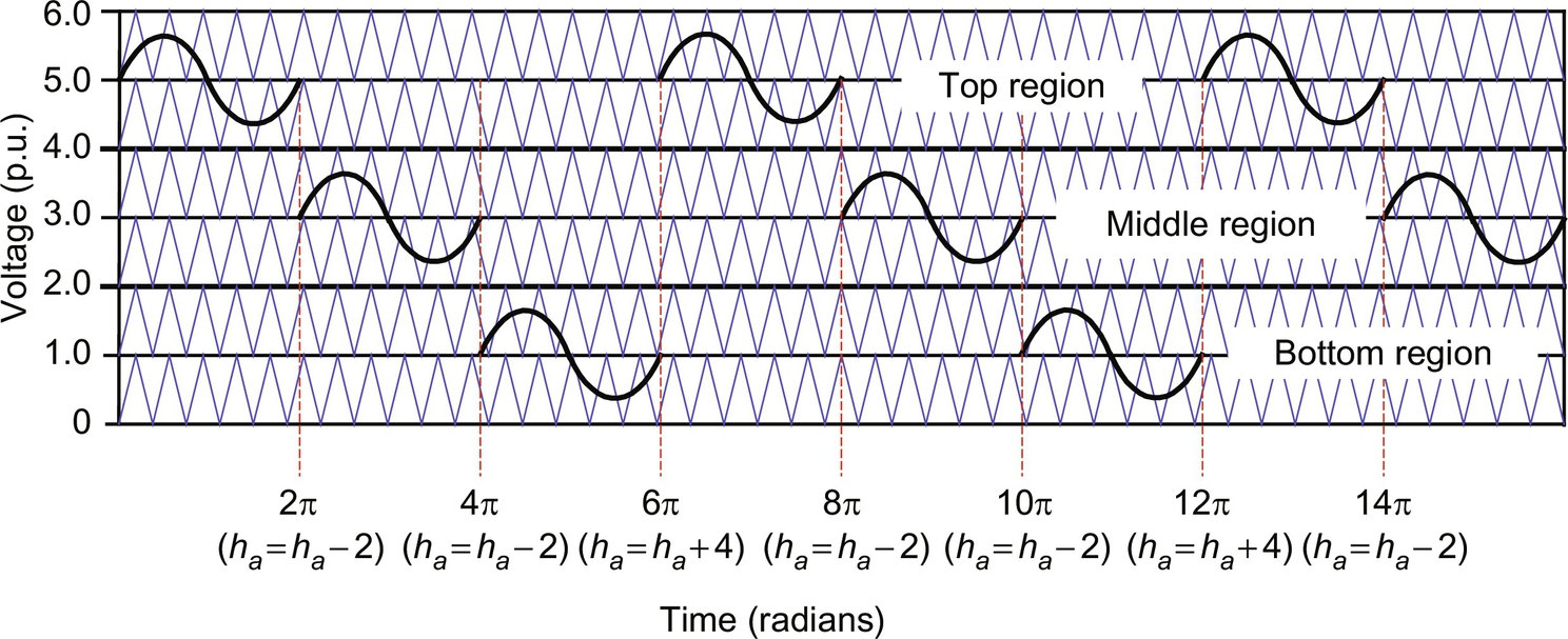
Fig. 13.6 shows one of the three line-line voltage waveforms for a six-level inverter. The line voltage Vab consists of a phase-leg “a” voltage and a phase-leg “b” voltage. The resulting line voltage is an 11-level staircase waveform. This means that an m-level diode-clamped inverter has an m-level output phase voltage and a (2m−1)-level output line voltage.

Although each active switching device is required to block only a voltage level of Vdc, the clamping diodes require different ratings for reverse voltage blocking. Using phase a of Fig. 13.5 as an example, when all the lower switches ![]() through
through ![]() are turned on, D4 must block four voltage levels or 4Vdc. Similarly, D3 must block 3Vdc, D2 must block 2Vdc, and D1 must block Vdc. If the inverter is designed such that each blocking diode has the same voltage rating as the active switches, Dn will require n diodes in series; consequently, the number of diodes required for each phase would be
are turned on, D4 must block four voltage levels or 4Vdc. Similarly, D3 must block 3Vdc, D2 must block 2Vdc, and D1 must block Vdc. If the inverter is designed such that each blocking diode has the same voltage rating as the active switches, Dn will require n diodes in series; consequently, the number of diodes required for each phase would be ![]() . Thus, the number of blocking diodes is quadratically related to the number of levels in a diode-clamped converter [28].
. Thus, the number of blocking diodes is quadratically related to the number of levels in a diode-clamped converter [28].
One application of the multilevel diode-clamped inverter is an interface between a high-voltage dc transmission line and an ac transmission line [29]. Another application would be a variable speed drive for high-power medium-voltage (2.4–13.8 kV) motors as proposed in [3,6,19,28–30]. Several authors have proposed for the diode-clamped converter that static var compensation is an additional function. The main advantages and disadvantages of multilevel diode-clamped converters are as follows [1–3].
13.2.2.1 Advantages
• All the phases share a common dc bus, which minimizes the capacitance requirements of the converter. For this reason, a back-to-back topology is not only possible but also practical for uses such as a high-voltage back-to-back interconnection or an adjustable speed drive.
• The capacitors can be precharged as a group.
• Efficiency is high for fundamental frequency switching.
13.2.2.2 Disadvantages
• Real power flow is difficult for a single inverter because the intermediate dc levels will tend to overcharge or discharge without precise monitoring and control.
• The number of clamping diodes required is quadratically related to the number of levels, which can be cumbersome for units with a high number of levels.
13.2.3 Flying-Capacitor Multilevel Inverter
Meynard and Foch introduced a flying-capacitor-based inverter in 1992 [31]. The structure of this inverter is similar to that of the diode-clamped inverter except that instead of using clamping diodes, the inverter uses capacitors. The circuit topology of the flying-capacitor multilevel inverter is shown in Fig. 13.7. This topology has a ladder structure of dc side capacitors, where the voltage on each capacitor differs from that of the next capacitor. The voltage increment between two adjacent capacitor legs gives the size of the voltage steps in the output waveform.
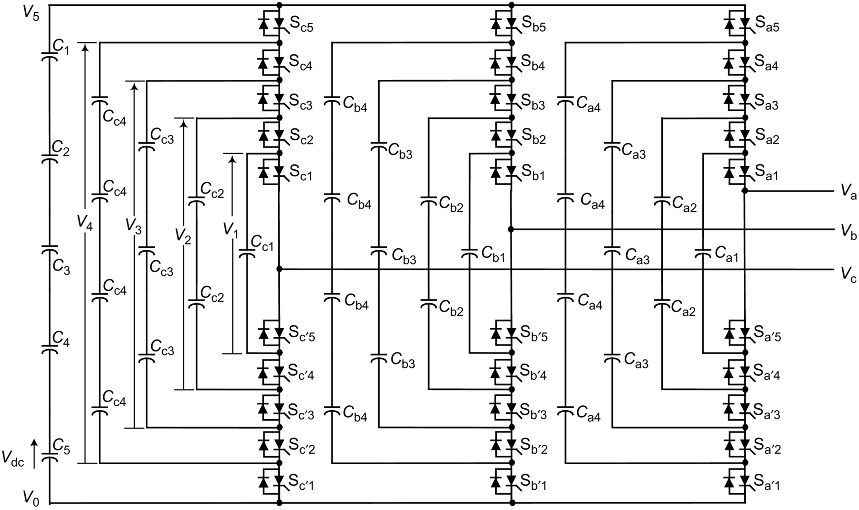
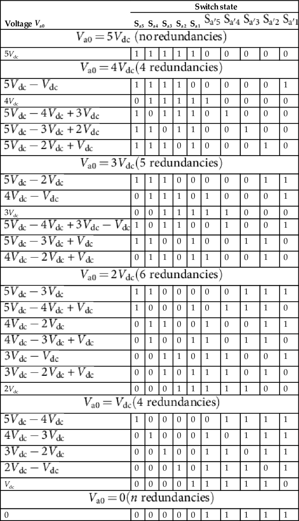
One advantage of the flying-capacitor-based inverter is that it has redundancies for inner voltage levels, that is, two or more valid switch combinations can synthesize an output voltage. Table 13.2 shows a list of all the combinations of phase voltage levels that are possible for the six-level circuit shown in Fig. 13.7. Unlike the diode-clamped inverter, the flying-capacitor inverter does not require all of the switches that are “on” (conducting) be in a consecutive series. Moreover, the flying-capacitor inverter has “phase” redundancies, whereas the diode-clamped inverter has only “line-line” redundancies [2,3,32]. These redundancies allow a choice of charging or discharging specific capacitors and can be incorporated in the control system for balancing the voltages across the various levels.
Table 13.2
Flying-capacitor six-level inverter redundant voltage levels and corresponding switch states
| Voltage Va0 | Switch state | |||||||||
| Sa5 | Sa4 | Sa3 | Sa2 | Sa1 | ||||||
| 5Vdc | 1 | 1 | 1 | 1 | 1 | 0 | 0 | 0 | 0 | 0 |
| 1 | 1 | 1 | 1 | 0 | 0 | 0 | 0 | 0 | 1 | |
| 4Vdc | 0 | 1 | 1 | 1 | 1 | 1 | 0 | 0 | 0 | 0 |
| 1 | 0 | 1 | 1 | 1 | 0 | 1 | 0 | 0 | 0 | |
| 1 | 1 | 0 | 1 | 1 | 0 | 0 | 1 | 0 | 0 | |
| 1 | 1 | 1 | 0 | 1 | 0 | 0 | 0 | 1 | 0 | |
| 1 | 1 | 1 | 0 | 0 | 0 | 0 | 0 | 1 | 1 | |
| 0 | 1 | 1 | 1 | 0 | 1 | 0 | 0 | 0 | 1 | |
| 3Vdc | 0 | 0 | 1 | 1 | 1 | 1 | 1 | 0 | 0 | 0 |
| 1 | 0 | 1 | 1 | 0 | 0 | 1 | 0 | 0 | 1 | |
| 1 | 1 | 0 | 0 | 1 | 0 | 0 | 1 | 1 | 0 | |
| 0 | 1 | 1 | 0 | 1 | 1 | 0 | 0 | 1 | 0 | |
| 1 | 1 | 0 | 0 | 0 | 0 | 0 | 1 | 1 | 1 | |
| 1 | 0 | 0 | 0 | 1 | 0 | 1 | 1 | 1 | 0 | |
| 0 | 1 | 1 | 0 | 0 | 1 | 0 | 0 | 1 | 1 | |
| 0 | 1 | 0 | 0 | 1 | 1 | 0 | 1 | 1 | 0 | |
| 0 | 0 | 1 | 1 | 0 | 1 | 1 | 0 | 0 | 1 | |
| 0 | 0 | 1 | 0 | 1 | 1 | 1 | 0 | 1 | 0 | |
| 2Vdc | 0 | 0 | 0 | 1 | 1 | 1 | 1 | 1 | 0 | 0 |
| 1 | 0 | 0 | 0 | 0 | 0 | 1 | 1 | 1 | 1 | |
| 0 | 1 | 0 | 0 | 0 | 1 | 0 | 1 | 1 | 1 | |
| 0 | 0 | 1 | 0 | 0 | 1 | 1 | 0 | 1 | 1 | |
| 0 | 0 | 0 | 1 | 0 | 1 | 1 | 1 | 0 | 1 | |
| Vdc | 0 | 0 | 0 | 0 | 1 | 1 | 1 | 1 | 1 | 0 |
| 0 | 0 | 0 | 0 | 0 | 0 | 1 | 1 | 1 | 1 | 1 |
In addition to the ![]() dc link capacitors, the m-level flying-capacitor multilevel inverter will require
dc link capacitors, the m-level flying-capacitor multilevel inverter will require ![]() auxiliary capacitors per phase if the voltage rating of the capacitors is identical to that of the main switches. One application proposed in the literature for the multilevel flying capacitor is static var generation [2,3]. The main advantages and disadvantages of multilevel flying-capacitor converters are as follows [2,3]:
auxiliary capacitors per phase if the voltage rating of the capacitors is identical to that of the main switches. One application proposed in the literature for the multilevel flying capacitor is static var generation [2,3]. The main advantages and disadvantages of multilevel flying-capacitor converters are as follows [2,3]:
13.2.3.1 Advantages
• Phase redundancies are available for balancing the voltage levels of the capacitors.
• Real and reactive power flow can be controlled.
• The large number of capacitors enables the inverter to ride through short duration outages and deep voltage sags.
13.2.3.2 Disadvantages
• Control is complicated to track the voltage levels for all of the capacitors. Also, precharging all of the capacitors to the same voltage level and start-up is complex.
• Switching utilization and efficiency is poor for real power transmission.
• The large number of capacitors is both more expensive and bulky than clamping diodes in multilevel diode-clamped converters. Packaging is also more difficult in inverters with a high number of levels.
13.2.4 Modular Mutilevel Inverter Structures
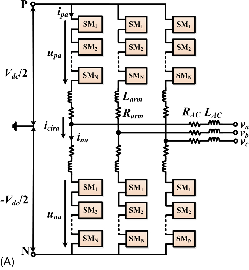
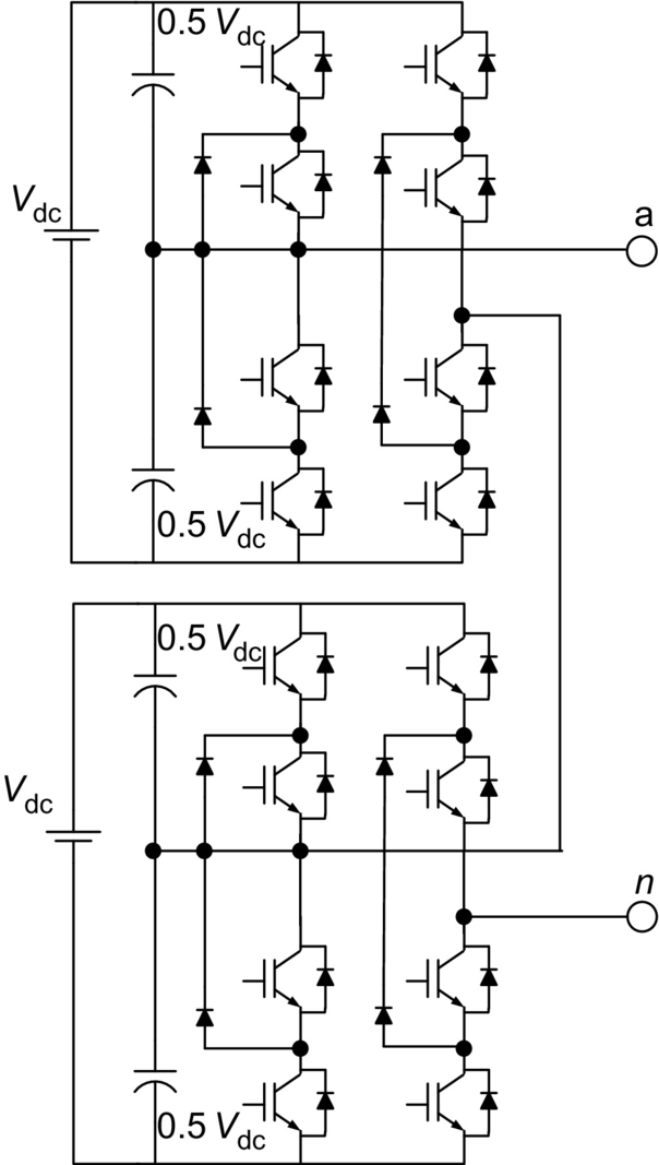
The modular multilevel converter (MMC) was first introduced by Marquardt in 2001 [33]. The configuration of a MMC is shown in Fig. 13.8A. Each phase leg of the MMC consists of one upper and one lower arm connected in series between the dc terminals. N series-connected SMs and one arm inductor Larm form an arm. Each SM can be realized by a half-bridge [34] [35], H-bridge [36] [37], or clamp-double [38] circuit, as illustrated in Fig. 13.8B–D.
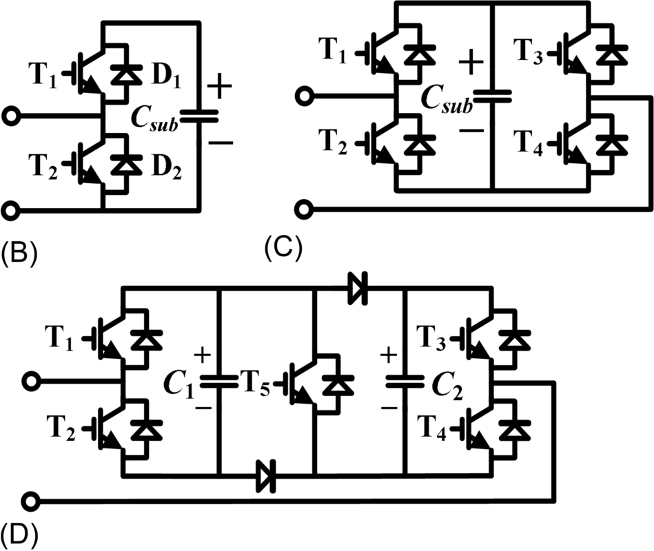
Among these, the MMC with half-bridge SM does not have any intrinsic fault current-limiting or current-blocking capability. Under a dc short-circuit fault, the fault current can flow from the ac side to the faulted dc side through the antiparalleled diodes of the controllable power switches, even though these switches are turned off. Therefore, fast-acting dc breakers are necessary to protect the system from damage. On the other hand, the H-bridge SM is capable of generating negative capacitor voltage, which can be used to block the fault current. However, compared with the half-bridge SM, the H-bridge one has twice the number of semiconductor devices, leading to higher cost and operating losses. For the “clamp-double” SM in Fig. 13.8D, power device T5 always conducts under normal operation conditions, making the clamp-double SM equivalent to two series-connected half-bridge SMs. Under a dc side fault, T5 is turned off, and dc voltage is inserted by both capacitors to minimize the dc fault current. Compared with the H-bridge SM, the output voltage of clamp-double SM can be doubled, with additional conduction loss of T5.
Due to the lower cost and higher efficiency, the MMC with half-bridge SMs is used for most of the commercial HVDC projects [39]. Therefore, the basic operation principle of an MMC with half bridge will be introduced in this section. As illustrated in Fig. 13.9B, each half-bridge SM contains two IGBTs as switching elements and a DC storage capacitor Csub. A SM is considered to be bypassed if the lower switch is closed and the upper switch is open, while if the lower switch is open and the upper switch is closed, the SM is inserted. Three different states are relevant for the proper operation of an SM, as illustrated in Fig. 13.9:


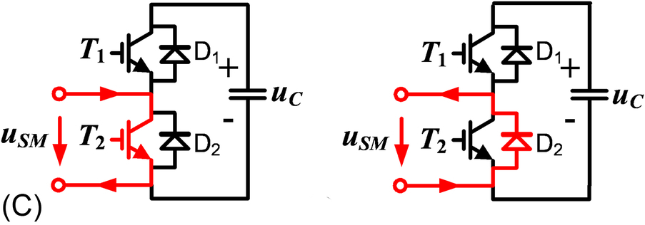
1. Both IGBTs are switched off.
This case does not occur during normal operation with power transfer. Upon charging, that is, after closing the AC power switch, all SMs of the converter are under this condition. In the event of a serious failure, all SMs of the converter should return to this state. If the current flows from the AC terminal to the dc side during this state, the flow passes through diode D1 and charges the capacitor. When it flows in the opposite direction, the freewheeling diode D2 conducts and bypasses the capacitor.
2. IGBT1 (T1) is switched on, and IGBT2 (T2) is switched off.
Irrespective of the current flow direction, the voltage of the storage capacitor is applied to the terminals of the SM. Depending on the current direction, the current either flows through D1 and charges the SM capacitor or flows through T1 and discharges the SM capacitor.
3. IGBT1 is switched off, and IGBT2 is switched on.
In this case, the current flows through either T2 or D2 depending on its direction, which ensures that zero voltage is applied to the terminals of the SM. The voltage in the capacitor remains unchanged.
It is thereby possible to separately and selectively control each of the individual SMs in a converter leg. In principle, the two converter arms of each phase represent a controllable voltage source. In this arrangement, the total voltage generated by the upper and lower arm SMs in one phase unit should equal to the dc link voltage. By adjusting the output voltage of SMs in both arms, that is, inserting and bypassing of SM capacitors according to a switching pattern created by a modulator, the desired sinusoidal voltage at the AC terminal can easily be achieved.
Fig. 13.10 illustrates the equivalent circuit of the MMC. Larm and Rarm are the arm inductance and equivalent arm resistance, respectively. Vdc and Idc are the total dc bus voltage and dc current individually. uvj is the converter output voltage of j phase at point v, whereas ivj is the corresponding line current. The arm voltages generated by the cascaded SMs are expressed as upj and unj, where the subscripts p and n denote the upper (positive) and lower (negative) arms, respectively. ipj and inj are the corresponding arm currents, which can be expressed as
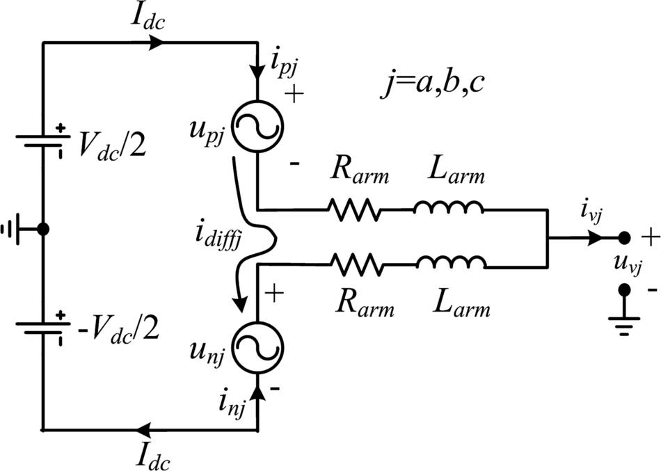

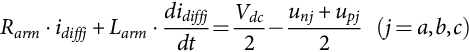
where idiffj denotes the inner circulating current of phase j, which flows through both the upper and lower arms and is given as
According to [40], the MMC can be characterized by the following equations:

where ej in (13.5) is the inner emf generated in a phase and
According to (13.5), when uvj is regarded as the ac network voltage, the current ivj can be controlled directly by regulating the control variable ej. The inner dynamic performance of the MMC is characterized by (13.6) and can be redefined as

where udiffj is the inner unbalance voltage of phase j.
According to (13.8), the circulating current idiffj can be controlled by regulating the unbalance voltage udiffj. Combining (13.7) and (13.8), the arm voltage references are
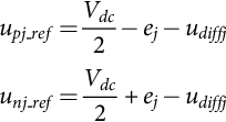
Because the same voltage udiffj is subtracted from upj_ref and unj_ref, according to (13.5) and (13.7), the resulting ej will not change, and thus, the ac side dynamics are not affected. As previously described, the reference of ej is generated from the traditional system control loops, whereas the inner unbalance voltage udiffj is used to control the MMC inner dynamic performance including the three-phase inner circulating currents.
Due to its unique structure, MMC has two typical issues, which will be discussed in the following sections.
(1) SM capacitor voltage balancing
According to the operating principle described above, the arm current in an MMC will only flow through the SM capacitor when the upper switch turns on and the SM is inserted. However, determined by various modulation schemes, the switching state for SMs is different from each other, leading to different charging/discharging times of the SM capacitors and thus voltage deviations. These unbalanced SM capacitor voltages generate the output voltage distortion and bring high-voltage stress to SM capacitors, as illustrated in Fig. 13.11. To address this issue, several voltage-balancing control schemes have been proposed over the last decade.
In [41], a voltage-balancing control consisting of an averaging control, individual-balancing control, and arm-balancing control was proposed for phase-shifted modulation schemes. The most widely accepted voltage-balancing control is based on a sorting method [42] [43]. The selection criteria are based on (1) SM capacitor voltages and (2) the direction of the arm currents. If the arm current is charging the capacitors, the SMs with the lowest capacitor voltages will be inserted. On the other hand, if the arm current is discharging the capacitors, the SMs with the highest capacitor voltages will be inserted. With this algorithm, the SM capacitor voltages can be well balanced. Here, the total SMs that need to be inserted can be calculated based on different modulation schemes introduced earlier.
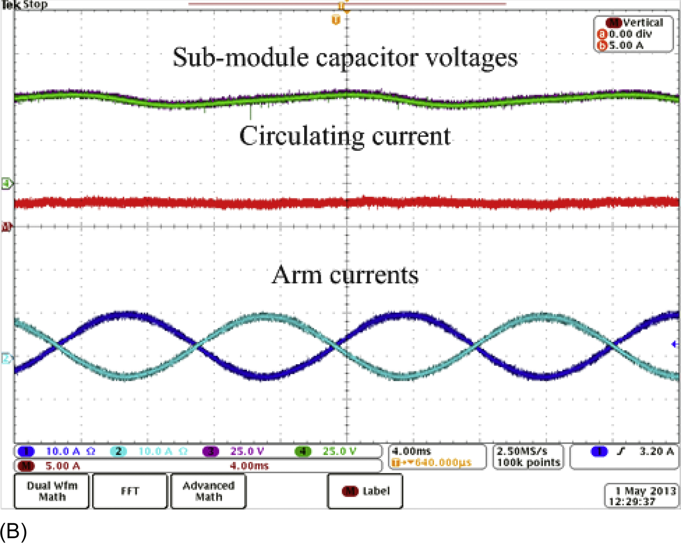
The main disadvantage of the above algorithms is the unnecessary switching actions of the SMs. Even if the capacitor voltage deviation is quite low and/or the number of required on-state SMs keep the same within two consecutive control periods, the SM insertion and bypassing may still occur, leading to increased switching frequency and loss. A modified sorting method has been proposed in [44] to avoid the high switching frequency, as shown in Fig. 13.12. In this method, a voltage deviation threshold is set, and the SM switching states only vary under the following two cases:


Case 1: The voltage deviation is larger than the predefined threshold (Vth).
Case 2: Different number of SMs need to be inserted.
In Case 1, two SM operation status will be changed based on the arm current direction. If the arm current is charging the capacitors, the SM with the highest capacitor voltage will be bypassed, and the SM with the lowest capacitor voltage will be inserted. If the current is discharging the capacitors in that arm, the SM with the lowest capacitor voltage is bypassed, and the SM with the highest capacitor voltage is inserted. For Case 2, an additional SM will be inserted or bypassed, and the same SM selection scheme in Case 1 is utilized. Due to its easy implementation and reduced switching losses, this modified sorting method with a capacitor voltage deviation threshold is widely used for MMC control.
(2) Circulating current control
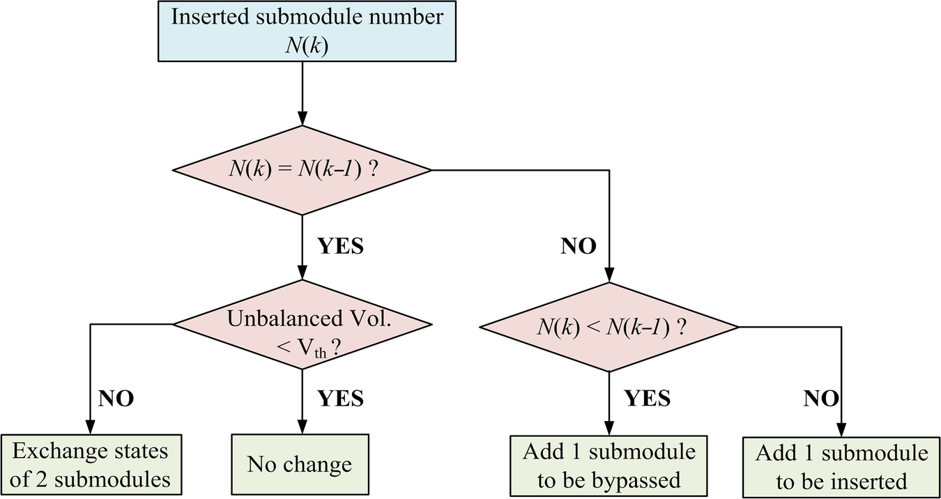
According to (13.6), if the SM capacitor voltage in Fig. 13.8 equals to Vdc/N (Vdc is dc link voltage, and N is SM number per arm) all the time, no circulating current will be generated. However, in a real MMC converter, low-frequency voltage ripples exist due to alternating arm current. For modulation schemes assuming constant SM capacitor voltages, for example, the direct modulation in [43], the inserted SM voltages in different half bridges could be different, inducing circulating current among the three phases. The circulating current will not affect the ac output voltage and currents. However, if it is not effectively suppressed, it increases the peak and RMS values of the arm currents, leading to high power losses and large SM capacitor voltage ripples. Under normal operation conditions, the dominant circulating current is negative sequence with second-order harmonic frequency [45,46]. Although the circulating current can be effectively mitigated by increasing the arm inductance, active suppression control schemes are preferred for lower converter volume and cost. A comparative experimental result with and without circulating current suppression control is given in Fig. 13.13 as an example.
Several circulating current suppressing control schemes have been proposed to reduce the circulating current in an MMC [47,48]. The basic idea of these control schemes is injecting a common mode arm voltage to counteract the submodule capacitor voltage variation. In the indirect modulation schemes proposed in [49,50], the sum of instantaneous capacitor voltages instead of the constant dc link voltage is used for insertion index calculation. In addition, the calculated or estimated total capacitor energy and the unbalanced arm energy are regulated, which inherently limit the circulating current. The second-order circulating current was transformed to d-q coordinates and controlled by a pair of PI controllers in [47]. During normal conditions, the dominant negative sequence second-order circulating current becomes dc components under d-q coordinates and can be eliminated without steady-state error. However, under ac grid unbalanced conditions, positive and/or zero-sequence circulating current will also be generated, which are ac components under the previous d-q coordinates and cannot be completely removed [51]. As a solution, proportional-resonant (PR)-based controllers were developed in [52,53], targeting elimination of all second-order components in circulating current under abc or αβ coordinates.

13.2.4.1 Advantages
• The number of SMs in each arm depends on the HVDC voltage level and individual IGBT device voltage. For example, with N series-connected SMs per arm, voltage rating of devices is reduced to Vdc/N (Vdc is dc link voltage), which eliminates the direct series connection of devices in two- and three-level converters. Given that the IGBT ratings are in kV level and HVDC rating is typically in hundreds of kV, often several hundred SMs are used for one MMC [54].
• Higher quality output voltage. With higher number of SMs in each arm (N), the output phase voltage of MMC becomes much more sinusoidal, which enables smaller ac filters, lower cost and compact converter footprint, as illustrated in Fig. 13.14.

• Lower switching frequency and higher efficiency. The series connection of N SMs per arm can achieve an equivalent switching frequency of Nfc (fc represents carrier frequency of each device) in the output voltage. In practical applications, the device average switching frequency is generally below 200 Hz. Consequently, state-of-the-art MMC-HVDC has loss level about 1%, close to that of LCC.
• Lower high-frequency noise due to reduced dv/dt and di/dt.
• Modular design and inherent redundancy. The modular design of MMC contributes to lower cost, shorter manufacturing as well as maintenance period, and high extensibility for higher voltage and power applications. Furthermore, the system becomes more reliable since failed SMs can be easily replaced by redundant ones [55].
The comparison of site footprint, building area, and building volumes for LCC-HVDC (Grita project, 500 MW and 400 kV), two-level VSC-HVDC, and half-bridge MMC-HVDC (EWIC project, 500 MW and ±200 kV) is presented in Table 13.3, using the Grita project as the 100% reference [56]. Different from LCC-HVDC, the converter reactors and dc yard equipment in VSC-HVDC are mounted in converter buildings, which provide more convenient maintenance, improved personal safety, lower high-frequency emissions and acoustic noise, and protection for equipment from adverse weather.
Table 13.3
Comparison of site areas among LCC and two-level VSC- and MMC-based HVDC systems [56]
| Site footprint | Site area (%) | Max building height (%) | Converter building footprint | Converter building area (%) | Converter building volume (%) | |
| LCC-HVDC (reference) | 225 m×120 m | 27,000 m2 (100%) | 20 m (100%) | 35 m×20 m | 700 m2 (100%) | 14,000 m2 (100%) |
| Two-level VSC | 180 m×115 m | 20,700 m2 (77%) | 24 m (120%) | 38 m×35 m | 1330 m2 (190%) | 25,000 m2 (179%) |
| Half-bridge MMC-HVDC | 165 m×95 m | 15,675 m2 (58%) | 15 m (75%) | 70 m×45 m | 2730 m2 (390%) | 29,500 m2 (211%) |

Without the requirement for reactive power compensation, the overall site area for two-level VSC-HVDC is 77% of that for LCC-HVDC, in spite of its higher converter building footprint, height, and volume. By adopting MMC, the site area is further reduced to only 58% of the reference value, and lower building height is achieved because of a decreased internal suspension height of converter valves. The overall site area reduction of MMC-HVDC supplies a significant benefit, especially for locations with restricted available area and/or high land price.
13.2.4.2 Disadvantages
• To meet the requirement for capacitor voltage ripple, Csub/N should be constant, which makes the power stage dimensioning quite difficult, especially for a MMC with numerous SMs per arm. Each SM requires a gate drive, protection, capacitor voltage monitoring, and associated communication resources, which greatly increase the cost of the system.
• The control scheme becomes much more complicated than that in a two-level converter. In addition to the generic upper level control to meet the overall system behavior requirements (Vdc-Q, P-Q, etc.), the capacitor voltage-balancing control and circulating current suppression control are indispensable in a MMC for desirable operation performance, and to lower the voltage and current stress applied on semiconductor devices and passive components. Because of the demand for accurate capacitor voltage and arm current detection and/or high-speed communication, these control schemes will introduce considerable expense and computing burden to the control unit.
13.2.5 Other Multilevel Inverter Structures
Besides the four basic multilevel inverter topologies discussed earlier, other multilevel converter topologies have been proposed; however, most of these are “hybrid” circuits that are combinations of two of the basic multilevel topologies or slight variations to them. In addition, the combination of multilevel power converters can be designed to match with a specific application based on the basic topologies. In the interest of completeness, some of these will be identified and briefly described.
13.2.4.1 Generalized Multilevel Topology
Existing multilevel converters such as diode-clamped and capacitor-clamped multilevel converters can be derived from the generalized converter topology called P2 topology proposed by Peng [57] as shown in Fig. 13.15. The generalized multilevel converter topology can balance each voltage level by itself regardless of load characteristics, active or reactive power conversion, and without any assistance from other circuits at any number of levels automatically. Thus, the topology provides a complete multilevel topology that embraces the existing multilevel converters in principle.

Fig. 13.15 shows the P2 multilevel converter structure per phase leg. Each switching device, diode, or capacitor's voltage is 1Vdc, for instance, ![]() of the dc link voltage. Any converter with any number of levels, including the conventional bilevel converter, can be obtained using this generalized topology [1,57].
of the dc link voltage. Any converter with any number of levels, including the conventional bilevel converter, can be obtained using this generalized topology [1,57].
13.2.4.2 Mixed-Level Hybrid Multilevel Converter
To reduce the number of separate dc sources for high-voltage, high-power applications with multilevel converters, diode-clamped or capacitor-clamped converters can be used to replace the full-bridge cell in a cascaded converter [58]. An example is shown in Fig. 13.16. The nine-level cascade converter incorporates a three-level diode-clamped converter as the cell. The original cascaded H-bridge multilevel converter requires four separate dc sources for one phase leg and 12 for a three-phase converter. If a five-level converter replaces the full-bridge cell, the voltage level is effectively doubled for each cell. Thus, to achieve the same nine voltage levels for each phase, only two separate dc sources are needed for one phase leg and six for a three-phase converter. The configuration has mixed-level hybrid multilevel units because it embeds multilevel cells as the building block of the cascade converter. The advantage of the topology is it needs less separate dc sources. The disadvantage for the topology is its control will be complicated due to its hybrid structure.
13.2.4.3 Soft-Switched Multilevel Converter
Some soft-switching methods can be implemented for different multilevel converters to reduce the switching loss and to increase efficiency. For the cascaded converter, because each converter cell is a bilevel circuit, the implementation of soft switching is not at all different from that of conventional bilevel converters. For capacitor-clamped or diode-clamped converters, soft-switching circuits have been proposed with different circuit combinations. One of the soft-switching circuits is a zero-voltage-switching type that includes auxiliary resonant commutated pole (ARCP), coupled inductor with zero-voltage transition (ZVT), and their combinations [1,59] as shown in Fig. 13.17.

13.2.4.4 Back-to-Back Diode-Clamped Converter
Two multilevel converters can be connected in a back-to-back arrangement, and then, the combination can be connected to the electric system in a series-parallel arrangement as shown in Fig. 13.18. Both the current demanded from the utility and the voltage delivered to the load can be controlled at the same time. This series-parallel active power filter has been referred to as a universal power conditioner [60–66] when used on electric distribution systems and as a universal power flow controller [67–71] when applied at the transmission level. Earlier, Lai and Peng [29] proposed the back-to-back diode-clamped topology shown in Fig. 13.19 for use as a high-voltage dc interconnection between two asynchronous ac systems or as a rectifier or inverter for an adjustable speed drive for high-voltage motors. The diode-clamped inverter has been chosen over the other two basic multilevel circuit topologies for use in a universal power conditioner for the following reasons:


• All six phases (three on each inverter) can share a common dc link. Conversely, the cascade inverter requires that each dc level to be separate, and this is not conducive to a back-to-back arrangement.
• The multilevel flying-capacitor converter also shares a common dc link; however, each phase leg requires several additional auxiliary capacitors. These extra capacitors would add substantially to the cost and the size of the conditioner.
Because a diode-clamped converter acting as a universal power conditioner will be expected to compensate for harmonics and/or operate in low-amplitude modulation index regions, a more sophisticated higher frequency switch control than the fundamental frequency switching method will be needed. For this reason, multilevel space vector and carrier-based PWM approaches are compared in the next section and novel carrier-based PWM methodologies are given.
13.3 Multilevel Converter PWM Modulation Strategies
Pulse-width modulation strategies used in a conventional inverter can be modified to use in multilevel converters. The advent of the multilevel converter PWM modulation methodologies can be classified according to switching frequency as shown in Fig. 13.20. The three multilevel PWM methods most discussed in the literature have been multilevel carrier-based PWM, selective harmonic elimination, and multilevel space vector PWM, which are all extensions of traditional two-level PWM strategies to several levels. Other multilevel PWM methods have been used to a much lesser extent by researchers; therefore, only the three major techniques will be discussed in detail in this chapter.

On the other hand, for MMC with tens to hundreds of SMs, new modulation schemes, for example, nearest level control (NLC), have been proposed for lower switching frequency and easy implementation, which will also be introduced in this chapter.
13.3.1 Multilevel Carrier-Based PWM
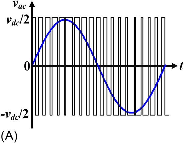
Several different two-level, carrier-based PWM techniques have been extended to multiple levels as a means for controlling the active devices in a multilevel converter. The most popular and easiest technique to implement uses several triangle carrier signals and one reference, or modulation, signal per phase. Fig. 13.21 illustrates three major techniques used in a conventional inverter that can be applied in a multilevel inverter: sinusoidal PWM (SPWM), third-harmonic injection PWM (THPWM), and space vector PWM (SVM). SPWM is a very popular method in industrial applications.

In order to achieve better dc link utilization at high modulation indexes, the sinusoidal reference signal can be injected by a third harmonic with a magnitude equal to 15% of the fundamental; its line-line output voltage is shown in Fig. 13.21B. As can be seen in Fig. 13.21B and C, the reference signals have some margin at unity amplitude modulation index. Obviously, the dc utilization of THPWM and SVM are better than SPWM in the linear modulation region. The dc utilization means the ratio of the output fundamental voltage to the dc link voltage. Other interesting carrier-based multilevel PWM are subharmonic PWM (SH-PWM) and switching frequency optimal PWM (SFO-PWM). Some particular aspects of these carrier-based methods are discussed as follows.
13.3.1.1 Subharmonic PWM
Carrara et al. [72] extended SH-PWM to multiple levels as follows: for an m-level inverter, ![]() carriers with the same frequency fc and the same amplitude Ac are disposed such that the bands they occupy are contiguous. The reference waveform has peak-to-peak amplitude Am, a frequency fm, and its zero centered in the middle of the carrier set. The reference signal is continuously compared with each of the carrier signals. If the reference signal is greater than a carrier signal, then the active device corresponding to that carrier is switched on, and if the reference signal is lesser than a carrier signal, then the active device corresponding to that carrier is switched off.
carriers with the same frequency fc and the same amplitude Ac are disposed such that the bands they occupy are contiguous. The reference waveform has peak-to-peak amplitude Am, a frequency fm, and its zero centered in the middle of the carrier set. The reference signal is continuously compared with each of the carrier signals. If the reference signal is greater than a carrier signal, then the active device corresponding to that carrier is switched on, and if the reference signal is lesser than a carrier signal, then the active device corresponding to that carrier is switched off.
In multilevel inverters, the amplitude modulation index, ma, and the frequency ratio, mf, are defined as
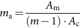

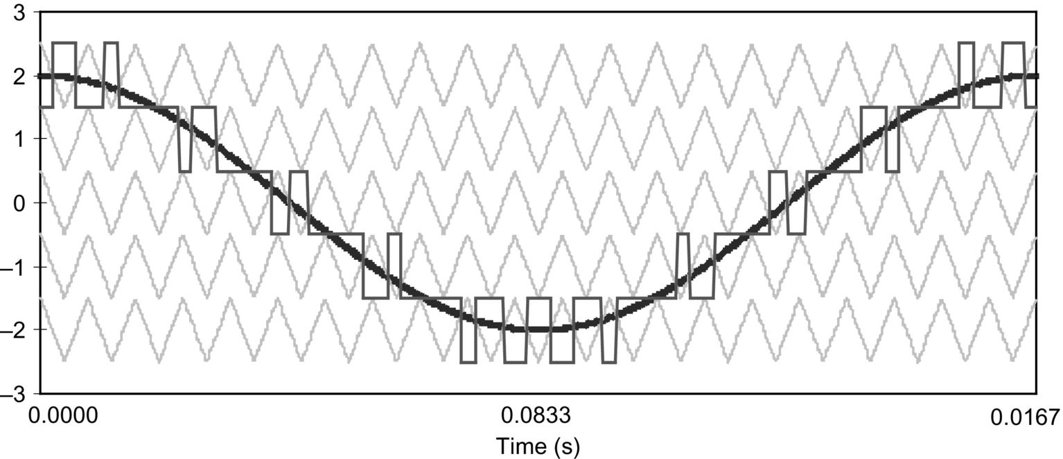
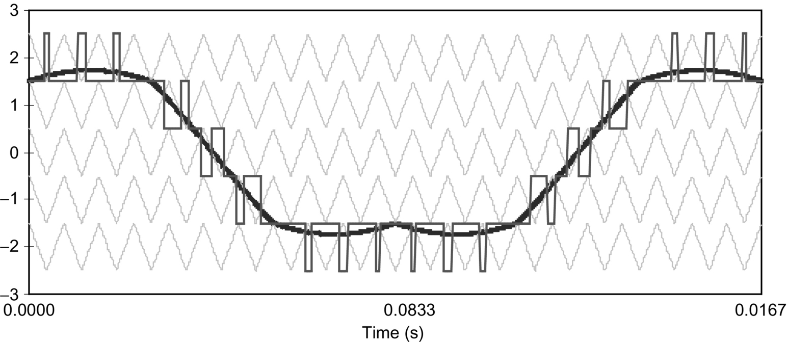
Fig. 13.22 shows a set of carriers ![]() for a six-level diode-clamped inverter and a sinusoidal reference or modulation waveform, with an amplitude modulation index of 0.8. Fig. 13.22 also shows the resulting output voltage of the inverter.
for a six-level diode-clamped inverter and a sinusoidal reference or modulation waveform, with an amplitude modulation index of 0.8. Fig. 13.22 also shows the resulting output voltage of the inverter.
 .
.13.3.1.2 Switching Frequency Optimal PWM
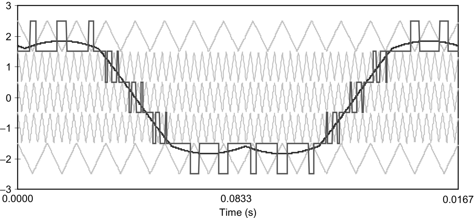
Another carrier-based method that was extended to multilevel applications by Menzies et al. is termed SFO-PWM, and it is similar to SH-PWM except that a zero-sequence (triplen harmonic) voltage is added to each of the carrier waveforms [73]. This method takes the instantaneous average of the maximum and minimum of the three reference voltages ![]() and subtracts this value from each of the individual reference voltages, that is,
and subtracts this value from each of the individual reference voltages, that is,
The addition of this triplen-offset voltage centers all of the three reference waveforms in the carrier band, which is equivalent to using space vector PWM [74,75]. The analog equivalent of Eqs. (13.12)–(13.15) is shown in Fig. 13.23 [76]. The SFO-PWM is shown in Fig. 13.24 for the same reference voltage waveform that was used in Fig. 13.22. The resulting output voltage of the inverter is also shown in Fig. 13.24. The SFO-PWM technique enables the modulation index to be increased by 15% before the overmodulation region is reached.

 .
.For the SH-PWM and SFO-PWM techniques shown in Figs. 13.22 and 13.24, the top and bottom switches are switched much more often than the intermediate devices. Methods to balance or reduce the device switchings without an adverse effect on a multilevel inverter's output voltage total harmonic distortion would be beneficial. The development of such methods is discussed in [77]. A novel method to balance device switchings for all of the levels in a diode-clamped inverter has been demonstrated for SH-PWM and SFO-PWM by varying the frequency for the different triangle wave carrier bands as shown in Fig. 13.25 [77].
 for Band2,
  ;
;  for Band1,
  ; Band0,
  ).
).13.3.1.3 Modulation Index Effect on Level Utilization
For low-amplitude modulation indexes, a multilevel inverter will not make use of all of its levels, and at very low modulation indexes, it operates as if it is a traditional two-level inverter. Fig. 13.26 shows two simulation results of what the output voltage waveform looks like at amplitude modulation indexes of 0.5 and 0.15. Fig. 13.26A shows how the bottom and top switches (![]() in Fig. 13.5) are unused for amplitude modulation indexes less than 0.6 in a six-level inverter. Fig. 13.26B shows how only the middle switches (
in Fig. 13.5) are unused for amplitude modulation indexes less than 0.6 in a six-level inverter. Fig. 13.26B shows how only the middle switches (![]() in Fig. 13.5) change states when a six-level inverter is operated at an amplitude modulation index less than 0.2. The output waveform in Fig. 13.26B appears to be that of a traditional two-level inverter rather than a multilevel inverter.
in Fig. 13.5) change states when a six-level inverter is operated at an amplitude modulation index less than 0.2. The output waveform in Fig. 13.26B appears to be that of a traditional two-level inverter rather than a multilevel inverter.

 and (B) SH-PWM,
 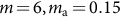 .
.The minimum modulation index ma min, for which a multilevel inverter controlled with SH-PWM makes use of all of its levels, m, is
Table 13.4 lists the minimum modulation index in which a multilevel inverter uses all its constituent levels for both SH-PWM and SFO-PWM techniques. Table 13.4 also shows that the maximum modulation index before pulse dropping (overmodulation) occurs is 1.000 for SH-PWM and 1.155 for SFO-PWM. As shown in Table 13.4, when a multilevel inverter operates at modulation indexes much less than 1.000, not all of its levels are involved in the generation of the output voltage and simply remain in an unused state until the modulation index increases sufficiently. The table also shows that level usage is more likely to suffer to a greater extent as the number of levels in the inverter increases.
Table 13.4
Modulation index ranges without level reduction (min) or pulse dropping because of overmodulation (max)
| Levels | SH-PWM | SFO-PWM | ||
| Min | Max | Min | Max | |
| 3 | 0.000 | 1.000 | 0.000 | 1.155 |
| 4 | 0.333 | 1.000 | 0.385 | 1.155 |
| 5 | 0.500 | 1.000 | 0.578 | 1.155 |
| 6 | 0.600 | 1.000 | 0.693 | 1.155 |
| 7 | 0.667 | 1.000 | 0.770 | 1.155 |
| 8 | 0.714 | 1.000 | 0.825 | 1.155 |
| 9 | 0.750 | 1.000 | 0.866 | 1.155 |
| 10 | 0.778 | 1.000 | 0.898 | 1.155 |
| 11 | 0.800 | 1.000 | 0.924 | 1.155 |
| 12 | 0.818 | 1.000 | 0.945 | 1.155 |
| 13 | 0.833 | 1.000 | 0.962 | 1.155 |
One way to make use of the multiple levels, even during low modulation periods, is to take advantage of the redundant output voltage states by rotating level usage in the inverter after each modulation cycle. This will reduce the switching stresses on some of the inner levels by making use of those outer voltage levels that otherwise would go unused.
As mentioned earlier, diode-clamped inverters have redundant line-line voltage states for low modulation indexes but have no phase redundancies [78]. For an output voltage state (i,j,k) in an m-level diode-clamped inverter, the number of redundant states available is given by
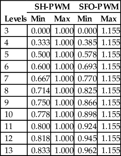
As the modulation index decreases, more redundant states are available. Table 13.5 shows the number of distinct and redundant line-line voltage states available in a six-level inverter for different output voltages.
Table 13.5
Six-level inverter line-line voltage redundancies
| Number of distinct states | Number of redundancies per distinct state | Total number of states | |
| 0 | 1 | 5 | 6 |
| 1 | 6 | 4 | 30 |
| 2 | 12 | 3 | 48 |
| 3 | 18 | 2 | 54 |
| 4 | 24 | 1 | 48 |
| 5 | 30 | 0 | 30 |
| Total | 91 | — | 216 |
In the next section, a carrier-based method is given that uses line-line redundancies in a diode-clamped inverter operating at a low modulation index so that active device usage is more balanced among the levels.
13.3.1.4 Increasing Switching Frequency at Low Modulation Indexes
For amplitude modulation indexes less than 0.5, the level usage in odd-level inverters can be sufficiently rotated so that the switching frequency can be doubled and still keep the thermal losses within the limits of the device. For inverters with an even number of levels, the modulation index at which frequency doubling can be accomplished varies with the levels as shown in Table 13.6. This increase in switching frequency enables the inverter to compensate for higher frequency harmonics and yields a waveform that more closely tracks a reference.
Table 13.6
Increased switching frequency possible at lower modulation indexes
| Inverter levels | Modulation index, ma | Frequency multiplier | |
| Min | Max | ||
| 3 | 0.000 | 0.500 | 2 |
| 4 | 0.000 | 0.333 | 3 |
| 5 | 0.250 | 0.500 | 2 |
| 0.000 | 0.250 | 4 | |
| 6 | 0.200 | 0.400 | 2 |
| 0.000 | 0.200 | 5 | |
| 7 | 0.333 | 0.500 | 2 |
| 0.167 | 0.333 | 3 | |
| 0.000 | 0.167 | 6 | |
| 8 | 0.285 | 0.428 | 2 |
| 0.142 | 0.285 | 3 | |
| 0.000 | 0.142 | 7 | |
| 9 | 0.25 | 0.500 | 2 |
| 0.125 | 0.250 | 4 | |
| 0.000 | 0.125 | 8 | |
| 10 | 0.333 | 0.444 | 2 |
| 0.222 | 0.333 | 3 | |
| 0.111 | 0.222 | 4 | |
| 0.000 | 0.111 | 9 | |
| 11 | 0.333 | 0.500 | 2 |
| 0.200 | 0.333 | 3 | |
| 0.000 | 0.200 | 5 | |
| 12 | 0.272 | 0.454 | 2 |
| 0.181 | 0.272 | 3 | |
| 0.090 | 0.181 | 5 | |
| 0.000 | 0.090 | 11 | |
| 13 | 0.333 | 0.500 | 2 |
| 0.250 | 0.333 | 3 | |
| 0.167 | 0.250 | 4 | |
| 0.0833 | 0.167 | 6 | |
| 0.000 | 0.0833 | 12 | |

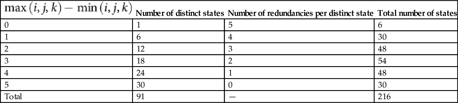
As an example of how to accomplish this doubling of inverter frequency, an analysis of a seven-level diode-clamped inverter with an amplitude modulation index of 0.4 is conducted. During the first cycle, the reference waveform is centered in the upper three carrier bands, and during the next cycle, the reference waveform is centered in the lower three carrier bands as shown in Fig. 13.27. This technique enables half of the switches to “rest” every other cycle and does not incur any switching losses. With this method, the switching frequency (or carrier frequency fc in the case of multilevel inverters) can effectively be doubled to 2fc, but the switches will have the same thermal losses as if they were switching at fc but every cycle.

 .
.This method is possible only for three-wire systems because the diode-clamped inverter has line-line redundancies and no phase redundancies. This means that at the discontinuity where the reference moves from one carrier band set to another, the transition has to be synchronized such that all three phases are moved from one carrier set to the next set at the same time. In the case of frequency doubling, all three phases add or subtract the following number of states (or levels) every other reference cycle:

At modulation indexes closer to zero, the switching frequency can be increased even more. This is possible because the reference waveform can be rotated among the carrier bands for a few cycles before returning to a previous set of switches for use. The switches are allowed to “rest” for a few cycles and thus are able to absorb higher losses during the cycle they are switched. Table 13.6 shows the possible increased switching frequencies available at lower amplitude modulation indexes for several different inverter levels.
Some additional switching loss is associated with the redundant switchings of the three phases at the end of each modulation cycle when rotating among carrier bands. For instance, for Fig. 13.28, each of the three phases in the seven-level inverter will have three switch pairs that change states at the end of every reference cycle. However, compared with the switching loss associated with just the normal PWM switchings, this redundant switching loss is quite small, typically less than 5% of the total switching loss.
 carrier frequency at very low modulation indexes.
Figs. 13.28 and 13.29 show two different methods of rotating the reference waveform among three different regions (top, middle, and bottom) for modulation indexes less than 0.333 in a seven-level inverter to enable the carrier frequency to be increased by a factor of three. The method shown in Fig. 13.28 is preferred over that shown in Fig. 13.29 because of less redundant state switching. The method shown in Fig. 13.28 requires only four redundant state switchings for every three reference cycles, whereas the method shown in Fig. 13.29 requires eight redundant switchings for every three reference cycles. In general, for any multilevel inverter regardless of the number of levels or number of rotation regions, using the preferred reference rotation method will have half of the redundant switching losses that the alternate method would have.
 carrier frequency at very low modulation indexes.
Unlike the diode-clamped inverter, the cascaded H-bridge inverter has phase redundancies in addition to the aforementioned line-line redundancies. Phase redundancies are much easier to exploit than line-line redundancies because the output voltage in each phase of a three-phase inverter can be generated independently of the other two phases when only phase redundancies are used. A method was given in [18] that makes use of these phase redundancies in a cascaded inverter so that duty cycle of each active device is balanced over ![]() modulation waveform cycles regardless of the modulation index. The same pulse rotation technique used for fundamental frequency switching of cascade inverters was used but with a PWM output voltage waveform [79], which is a much more effective means of controlling a driven motor at low speeds than continuing to do fundamental frequency switching. The effect of this control is that the output waveform can have a high switching frequency, but the individual levels can still switch at a constant switching frequency of 60 Hz if desired.
modulation waveform cycles regardless of the modulation index. The same pulse rotation technique used for fundamental frequency switching of cascade inverters was used but with a PWM output voltage waveform [79], which is a much more effective means of controlling a driven motor at low speeds than continuing to do fundamental frequency switching. The effect of this control is that the output waveform can have a high switching frequency, but the individual levels can still switch at a constant switching frequency of 60 Hz if desired.
13.3.1.5 Multicarrier Modulation Techniques for MMC
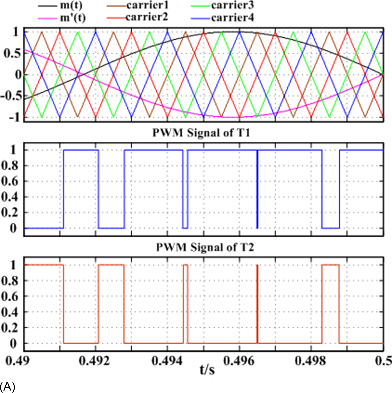
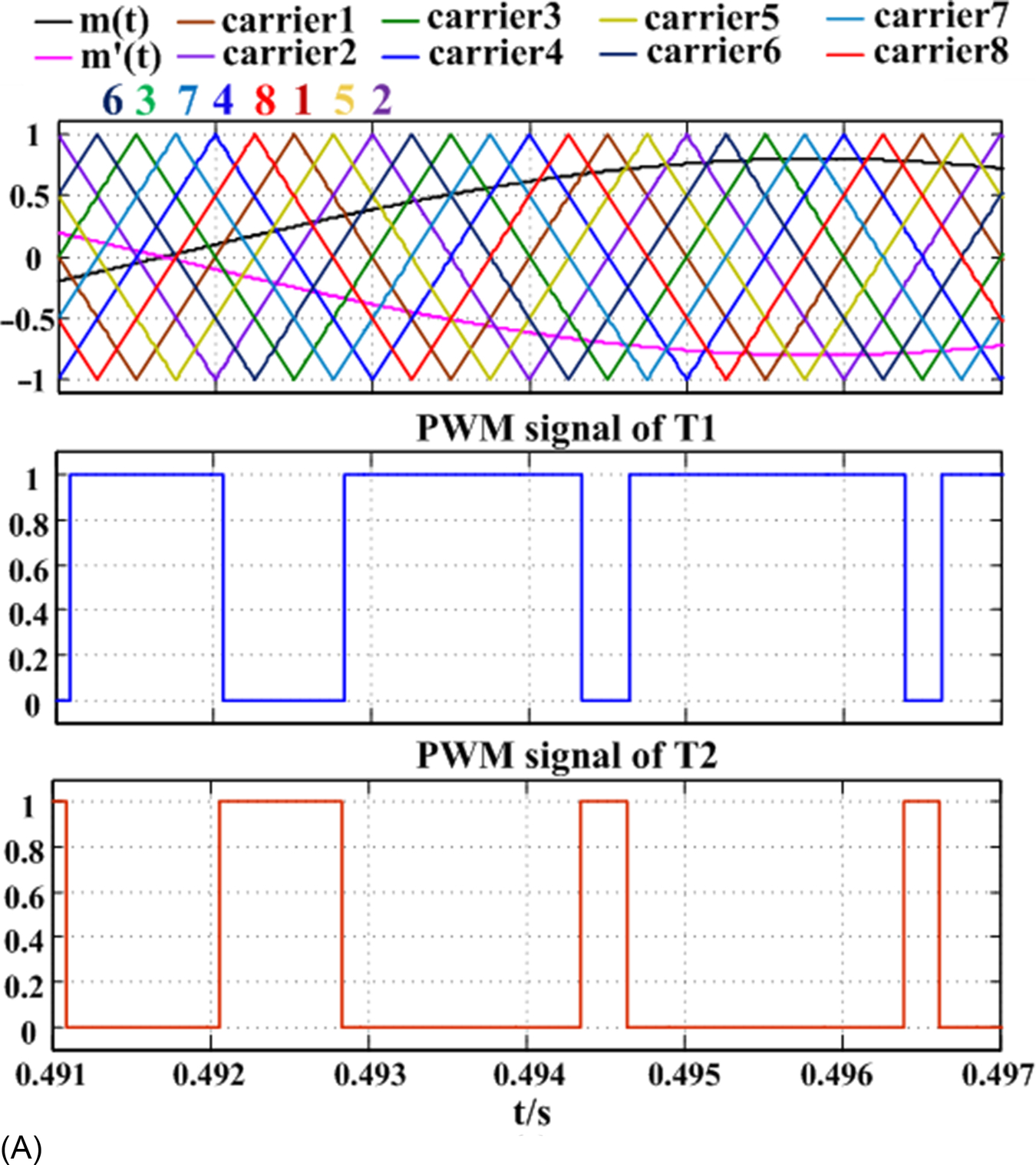
The multicarrier techniques have also been successfully extended for MMC by using multiple carriers to control power switches of the converter topologies. It is mainly divided into two types: (1) carrier phase-shifted PWM (CPS-PWM) and (2) carrier level-shifted PWM (CLS-PWM) [80,81].
(1) CPS-PWM
For an MMC with 2N cells, the carrier waves (either sawtooth or triangular waveforms) with a phase shift of 360 degrees/N or 180 degrees/N can be employed to generate the staircase multilevel output waveform with low distortion. The modulation and output voltage waveforms for N+1 and 2N+1 levels (N=4) are given in Figs. 13.30 and 13.31, respectively.
With N+1 level modulation scheme (phase shift of 360 degrees/N among carriers), N SMs per phase are inserted at all times, leading to a balanced capacitor voltage. In contrast, if 2N+1 level modulation scheme (phase shift of 180 degrees/N among carriers) is used, N+1 or N−1 SMs will be inserted at certain time, causing issues with the capacitor voltage self-balancing algorithm and requiring additional balancing control. Using PS-PWM modulation algorithm, the effective switching frequency of the load voltage will be much higher that of each cell (Nfc for N+1 level and 2Nfc for 2N+1 level, fc is the carrier frequency). This property allows low switching frequency of each SM, thus reducing switching losses. In addition, it enables a high degree of linearity, outstanding control performance, and other advantages.


(2) CLS-PWM
The carriers can also be arranged with shifts in amplitude, relating each carrier with the corresponding output voltage level generated by the multilevel inverter, which is the so-called level-shifted PWM (LS-PWM). Depending on the disposition of the carriers, three types of CLS-PWM have been developed: phase disposition (PD), phase opposition disposition (POD), and alternate phase opposition disposition (APOD), as shown in Fig. 13.32.
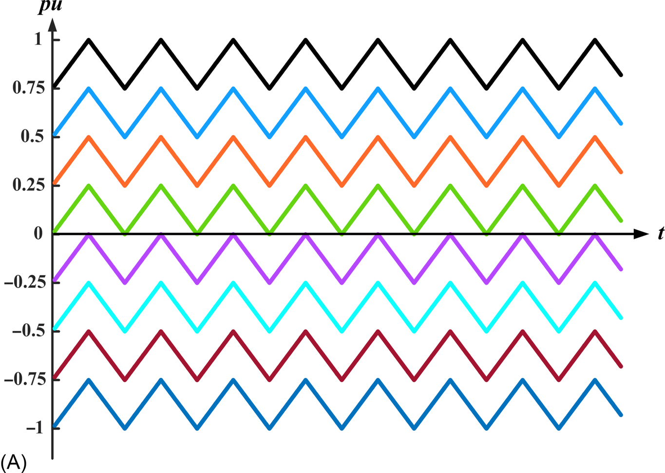
The PD-PWM method is realized through a comparison between a sinusoidal reference wave with vertically shifted carrier waves. N carrier signals will be created to generate an output voltage with N+1 levels. The carrier signals have the same amplitude and frequency, and all signals are in phase. In the POD-PWM method, all carrier signals above the zero axis (positive region) are in phase, and those below zero axis (negative region) are also in phase but 180 degrees phase shifted from the carrier waves in positive region. The APOD-PWM scheme requires N−1 carrier signals with phase shift of 180 degrees from each other.
The LS-PWM methods can be adopted for any multilevel converter topology. However, they are not very suitable for CHB (cascaded H-bridge converter) and MMC inverters. According to the modulation principle, the uppermost SMs will be inserted for a short time, while the middle ones insert for most of the time during a fundamental cycle, producing an uneven power dissipation and large capacitor voltage differences among the SMs.
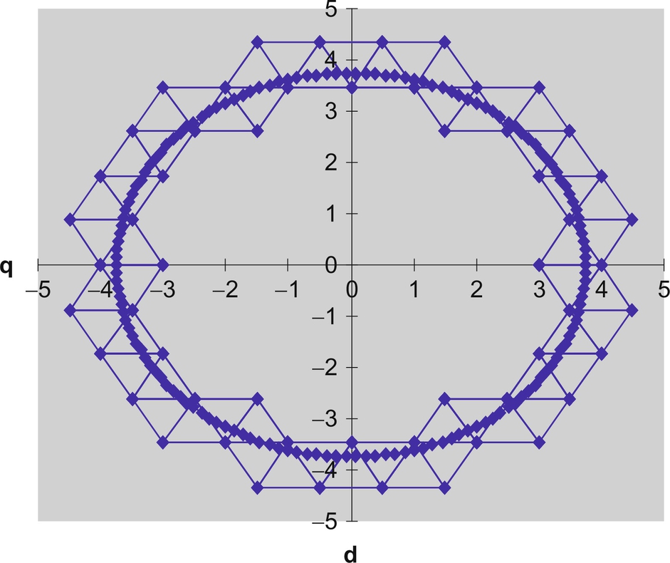
13.3.2 Multilevel Space Vector PWM
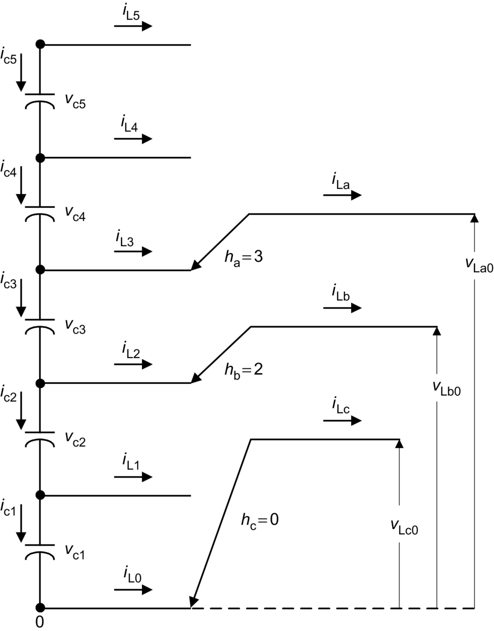
Choi et al. [82] were the first authors to extend the two-level space vector PWM technique to more than three levels for the diode-clamped inverter. Fig. 13.33 shows how the space vector d-q plane looks like for a six-level inverter. Fig. 13.34 represents the equivalent dc link of a six-level inverter as a multiplexer that connects each of the three output phase voltages to one of the dc link voltage tap points [83]. Each integral point on the space vector plane represents a particular three-phase output voltage state of the inverter. For instance, the point (3, 2, and 0) on the space vector plane means that with respect to ground, “a” phase is at 3Vdc, “b” phase is at 2Vdc, and “c” phase is at 0Vdc. The corresponding connections between the dc link and the output lines for the six-level inverter are also shown in Fig. 13.34 for the point (3, 2, 0). An algebraic way to represent the output voltages in terms of the switching states and dc link capacitors is described in the following [84]. For ![]() , where m is the number of levels in the inverter,
, where m is the number of levels in the inverter,

where

and

where ha is the switch state and j is an integer from 0 to n and where ![]() if
if ![]() if
if ![]() .
.
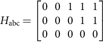
Besides the output voltage state, the point (3, 2, 0) on the space vector plane can also represent the switching state of the converter. Each integer indicates how many upper switches in each phase leg are on for a diode-clamped converter. As an example, for ![]() , the Habc matrix for this particular switching state of a six-level inverter would be
, the Habc matrix for this particular switching state of a six-level inverter would be
Redundant switching states are those states for which a particular output voltage can be generated by more than one switch combination. Redundant states are possible at lower modulation indexes or at any point other than those on the outermost hexagon shown in Fig. 13.33. Switch state (3, 2, 0) has redundant states (4, 3, 1) and (5, 4, 2). Redundant switching states differ from each other by an identical integral value, that is, (3, 2, 0) differs from (4, 3, 1) by (1, 1, 1) and from (5, 4, 2) by (2, 2, 2).
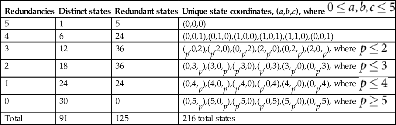
For an output voltage state (x,y,z) in an m-level diode-clamped inverter, the number of redundant states available is given by ![]() . As the modulation index decreases (or the voltage vector in the space vector plane gets closer to the origin), more redundant states are available. The number of possible zero states is equal to the number of levels, m. For a six-level diode-clamped inverter, the zero-voltage states are (0, 0, 0), (1, 1, 1), (2, 2, 2), (3, 3, 3), (4, 4, 4), and (5, 5, 5).
. As the modulation index decreases (or the voltage vector in the space vector plane gets closer to the origin), more redundant states are available. The number of possible zero states is equal to the number of levels, m. For a six-level diode-clamped inverter, the zero-voltage states are (0, 0, 0), (1, 1, 1), (2, 2, 2), (3, 3, 3), (4, 4, 4), and (5, 5, 5).
The number of possible switch combinations is equal to the cube of the level (m3). For this six-level inverter, there are 216 possible switching states. The number of distinct or unique states for an m-level inverter can be given by
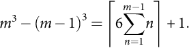
Therefore, the number of redundant switching states for an m-level inverter is ![]() . Table 13.7 summarizes the available redundancies and distinct states for a six-level diode-clamped inverter.
. Table 13.7 summarizes the available redundancies and distinct states for a six-level diode-clamped inverter.
Table 13.7
Line-line redundancies of six-level three-phase diode-clamped inverter
| Redundancies | Distinct states | Redundant states | Unique state coordinates, (a,b,c), where |
| 5 | 1 | 5 | (0,0,0) |
| 4 | 6 | 24 | (0,0,1),(0,1,0),(1,0,0),(1,0,1),(1,1,0),(0,0,1) |
| 3 | 12 | 36 | (p,0,2),(p,2,0),(0,p,2),(2,p,0),(0,2,p),(2,0,p), where |
| 2 | 18 | 36 | (0,3,p),(3,0,p),(p,3,0),(p,0,3),(3,p,0),(0,p,3), where |
| 1 | 24 | 24 | (0,4,p),(4,0,p),(p,4,0),(p,0,4),(4,p,0),(0,p,4), where |
| 0 | 30 | 0 | (0,5,p),(5,0,p),(p,5,0),(p,0,5),(5,p,0),(0,p,5), where |
| Total | 91 | 125 | 216 total states |
In two-level PWM, a reference voltage is tracked by selecting the two nearest voltage vectors and a zero vector and then by calculating the time required to be at each of these three vectors such that their sum equals the reference vector. In multilevel PWM, generally, the nearest three triangle vertices, V1,V2, and V3, to a reference point ![]() are selected to minimize the harmonic components of the output line-line voltage [85]. The respective time duration, T1,T2, and T3, required for these vectors is then solved from the following equations:
are selected to minimize the harmonic components of the output line-line voltage [85]. The respective time duration, T1,T2, and T3, required for these vectors is then solved from the following equations:
where Ts is the switching period. Eq. (13.21) actually represents two equations, one with the real part of the terms and one with the imaginary part of the terms:
Eqs. (13.22)–(13.25) can then be solved for T1,T2, and T3 as follows:

Others have proposed space vector methods that did not use the nearest three vectors, but these methods generally add complexity to the control algorithm. Fig. 13.35 shows what a sinusoidal reference voltage (circle of points) and the inverter output voltages look like in the d-q plane.
Redundant switch levels can be used to help manage the charge on the dc link capacitors [86]. Generalizing from Fig. 13.34, the equations for the currents through the dc link capacitors can be given as
and
The dc link currents for ![]() would be
would be ![]() . To see how redundant states affect the dc link currents, consider the two redundant states for (3, 2, 0). In state (4, 3, 1), the dc link currents would be
. To see how redundant states affect the dc link currents, consider the two redundant states for (3, 2, 0). In state (4, 3, 1), the dc link currents would be ![]() ; and for the state (5, 4, 2), the dc link currents would be
; and for the state (5, 4, 2), the dc link currents would be ![]() .
.
From this example, one can see that the choice of redundant switching states can be used to determine which capacitors will be charged/discharged or unaffected during the switching period. Although this control is helpful in balancing the individual dc voltages across the capacitors that make up the dc link, this method is quite complicated in selecting which of the redundant states to use. Constant use of redundant switching states also results in a higher switching frequency and lower efficiency of the inverter because of the extra switchings. Optimized space vector switching sequences for multilevel inverters have been proposed in [87].
13.3.3 Selective Harmonic Elimination
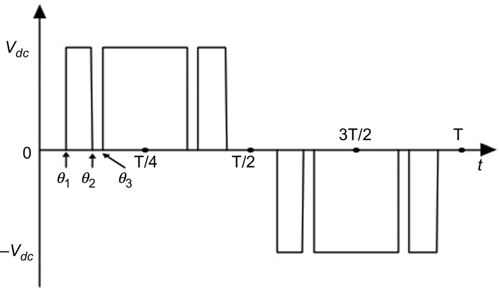
13.3.3.1 Fundamental Switching Frequency
The selective harmonic elimination method is also called fundamental switching frequency method based on the harmonic elimination theory proposed by Patel and Hoft [88,89]. A typical 11-level multilevel converter output with fundamental frequency switching scheme is shown in Fig. 13.2. The Fourier series expansion of the output voltage waveform as shown in Fig. 13.2 is expressed in Eqs. (13.1) and (13.2).
The conducting angles, θ1,θ2,…,θs, can be chosen such that the voltage total harmonic distortion is a minimum. Normally, these angles are chosen so as to cancel the predominant lower frequency harmonics [19].
For the 11-level case in Fig. 13.2, the fifth, seventh, eleventh, and thirteenth harmonics can be eliminated with the appropriate choice of the conducting angles. One degree of freedom is used so that the magnitude of the fundamental waveform corresponds to the reference waveform's amplitude or modulation index, ma, which is defined as ![]() is the amplitude command of the inverter for a sine wave output phase voltage, and VLmax is the maximum attainable amplitude of the converter, that is,
is the amplitude command of the inverter for a sine wave output phase voltage, and VLmax is the maximum attainable amplitude of the converter, that is, ![]() . The equations from Eq. (13.2) will now be as follows:
. The equations from Eq. (13.2) will now be as follows:

The above equations are nonlinear transcendental equations that can be solved by an iterative method such as the Newton-Raphson method. For example, using a modulation index of 0.8 obtains the following: ![]() . Thus, if the inverter output is symmetrically switched during the positive half cycle of the fundamental voltage to
. Thus, if the inverter output is symmetrically switched during the positive half cycle of the fundamental voltage to ![]() at
at ![]() at
at ![]() at
at ![]() at 45.14degrees and
at 45.14degrees and ![]() at 62.24degrees and similarly in the negative half cycle to
at 62.24degrees and similarly in the negative half cycle to ![]() at
at ![]() at
at ![]() at
at ![]() at
at ![]() at 242.24degrees, the output voltage of the 11-level inverter will not contain the 5th, 7th, 11th, and 13th harmonic components [18]. Other methods to solve these equations include using genetic algorithms [90] and resultant theory [91,92].
at 242.24degrees, the output voltage of the 11-level inverter will not contain the 5th, 7th, 11th, and 13th harmonic components [18]. Other methods to solve these equations include using genetic algorithms [90] and resultant theory [91,92].
Practically, the precalculated switching angles are stored as the data in memory (lookup table). Therefore, a microcontroller could be used to generate the PWM gate-drive signals. More recent methods have been developed that can generate the switching angles in real time using genetic algorithms.
13.3.3.2 Selective Harmonic Elimination PWM
In order to achieve a wide range of modulation indexes with minimized THD for the synthesized waveforms, a generalized selective harmonic modulation method [93,94] was proposed, which is called virtual stage PWM [90]. An output waveform is shown in Fig. 13.36. The virtual stage PWM is a combination of the unipolar programmed PWM and the fundamental frequency switching scheme. The output waveform of unipolar programmed PWM is shown in Fig. 13.37. When unipolar programmed PWM is employed on a multilevel converter, typically one dc voltage is involved, where the switches connected to the dc voltage are switched “on” and “off” several times per fundamental cycle. The switching pattern decides what the output voltage waveform looks like.

For fundamental switching frequency method, the number of switching angles is equal to the number of dc sources. However, for the virtual stage PWM method, the number of switching angles is not equal to the number of dc voltages. For example, in Fig. 13.36, only two dc voltages are used, whereas there are four switching angles.
Bipolar programmed PWM and unipolar programmed PWM could be used for modulation indexes too low for the applicability of the multilevel fundamental frequency switching method. Virtual stage PWM can also be used for low modulation indexes. Virtual stage PWM will produce output waveforms with a lower THD most of the time [90]. Therefore, virtual stage PWM provides another alternative to bipolar programmed PWM and unipolar programmed PWM for low modulation index control.
The major difficulty for selective harmonic elimination methods, including the fundamental switching frequency method and the virtual stage PWM method, is to solve the transcendental Eq. (13.28) for switching angles. Newton's method can be used to solve Eq. (13.28), but it needs good initial guesses, and solutions are not guaranteed. Therefore, Newton's method is not feasible to solving equations for large number of switching angles if good initial guesses are not available [95].
The resultant method has been proposed in [91,92,96] to solve the transcendental equations for switching angles. The transcendental equations characterizing the harmonic content can be converted into polynomial equations. Elimination resultant theory has been employed to determine the switching angles to eliminate specific harmonics, such as the 5th, 7th, 11th, and 13th. However, as the number of dc voltages or the number of switching angles increases, the degrees of the polynomials in these equations become bulky.
To overcome this problem, the fundamental frequency switching angle computation is solved by Newton's method. The initial guess can be provided by the results of lower order transcendental equations by the resultant method [95].
13.3.4 Other Modulation Strategies for Modular Multilevel Inverter
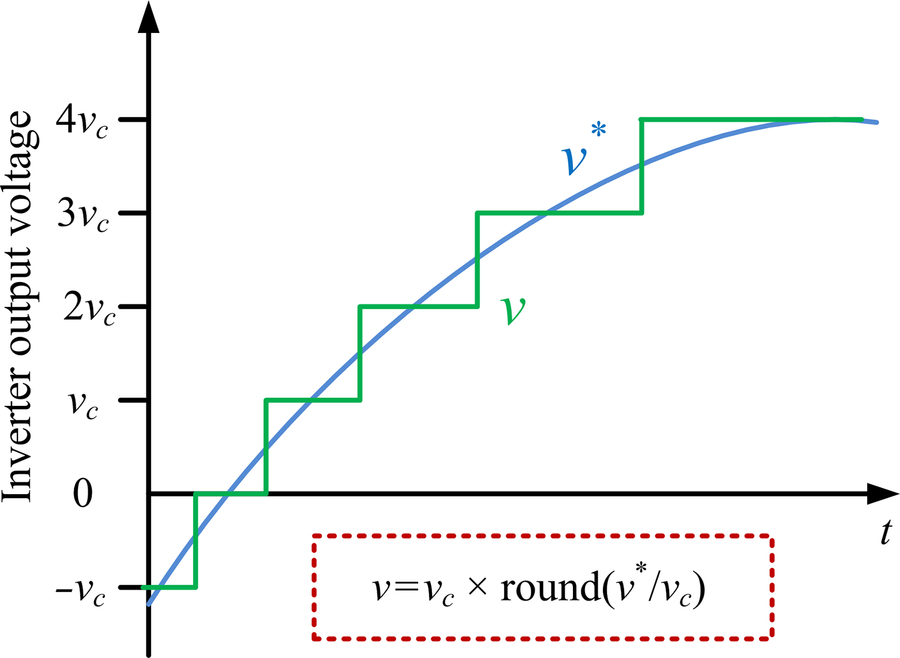
Space vector control (SVC) fully utilizes the large number of voltage vectors generated by multilevel converters, which approximates the voltage reference to the closest available state vector. This principle enables SVC with fundamental switching frequency and thus lower switching losses. Meanwhile, different from SHE PWM, the switching sequence can be produced online, resulting in a relatively easy implementation of SVC in closed-loop and high-bandwidth applications. The time domain version of SVC is the nearest level control (NLC), which approximates the closet voltage level instead of vector that can be generated by the converter, as illustrated in Fig. 13.38, where the inserted SM number equals to an integer closest to voltage reference v⁎ over SM capacitor voltage vc. The basic idea of NLC is to first calculate how many SMs should be inserted and which SMs will be determined by the capacitors' voltage sorting and the direction of the arm current.
Based on an approximation instead of a modulation, both SVC and NLC are suitable for inverters with a high number of levels. On the other hand, due to the low and variable switching frequency, these two methods suffer high total harmonic distortion (THD) when the voltage levels and/or modulation indexes are low.
In summary, each multilevel modulation scheme has its own uniqueness, making it more suitable for specific converter topologies and applications. In general, low switching frequency modulation methods are preferred for high-power applications due to lower switching loss, while high switching frequency algorithms enable better output power quality and higher bandwidth and thus are more suitable for high-dynamic-range applications.
13.4 Conclusion
This chapter has demonstrated the state of the art of multilevel power converter technology. Fundamental multilevel converter structures and modulation paradigms including the pros and cons of each technique have been discussed. Most of the chapter focuses on modern and more practical industrial applications of multilevel converters. The possible future enlargements of multilevel converter technology such as fault diagnosis system and renewable energy sources have been noted in earlier literature [97]. The development of wide bandgap power devices, especially medium-voltage SiC MOSFETs, IGBTs, diodes, and thyristors, in the next several years is expected to open more applications for multilevel converters. It should be noted that this chapter could not cover all multilevel, power converter-related applications; however, the basic principles of different multilevel converters have been discussed methodically. The main objective of this chapter is to provide a general notion to readers who are interested in multilevel power converters and their applications.