
35.3.5.7 Example 35.17: Sliding-Mode Vector Controllers for Matrix Converters
Matrix converters are all silicon ac/ac switching power converters, able to provide almost sinusoidal output voltages with adjustable amplitude and frequency, almost sinusoidal input currents, and controllable input power factor [22]. They have been used in ac drive speed control and are well suited for applications related to power-quality enhancement. The lack of an intermediate energy storage link results in high power density, their main advantage, but implies an input/output coupling that increases the control complexity.
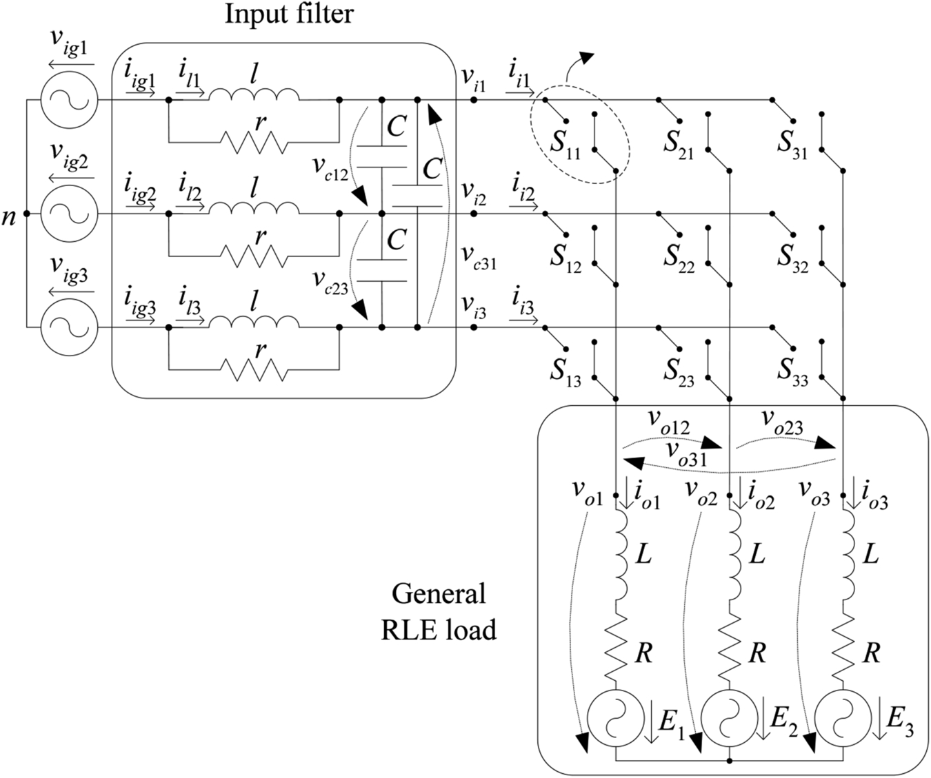
This example presents the design of sliding-mode controllers considering the switched state-space model of the matrix converter (nine bidirectional power switches), including the three-phase input filter and the output load (Fig. 35.64).
Output voltage control
Ideal three-phase matrix converters are obtained by assembling nine bidirectional switches, with the turn-off capability, to allow the connection of each one of the input phases to any one of the output phases (Fig. 35.64). The states of these switches are usually represented as a nine-element matrix S (Eq. (35.171)), in which each matrix element, Skj k, j∈{1, 2, 3}, has two possible states: Skj=1 if the switch is closed (ON) and Skj=0 if it is open (OFF). Only 27 switching combinations are possible (Table 35.6), as a result of the topological constraints (the input phases should never be short-circuited, and the output inductive currents should never be interrupted), which implies that the sum of all the Skj of each one of the matrix, k rows, must always equal to 1 (Eq. (35.171)):
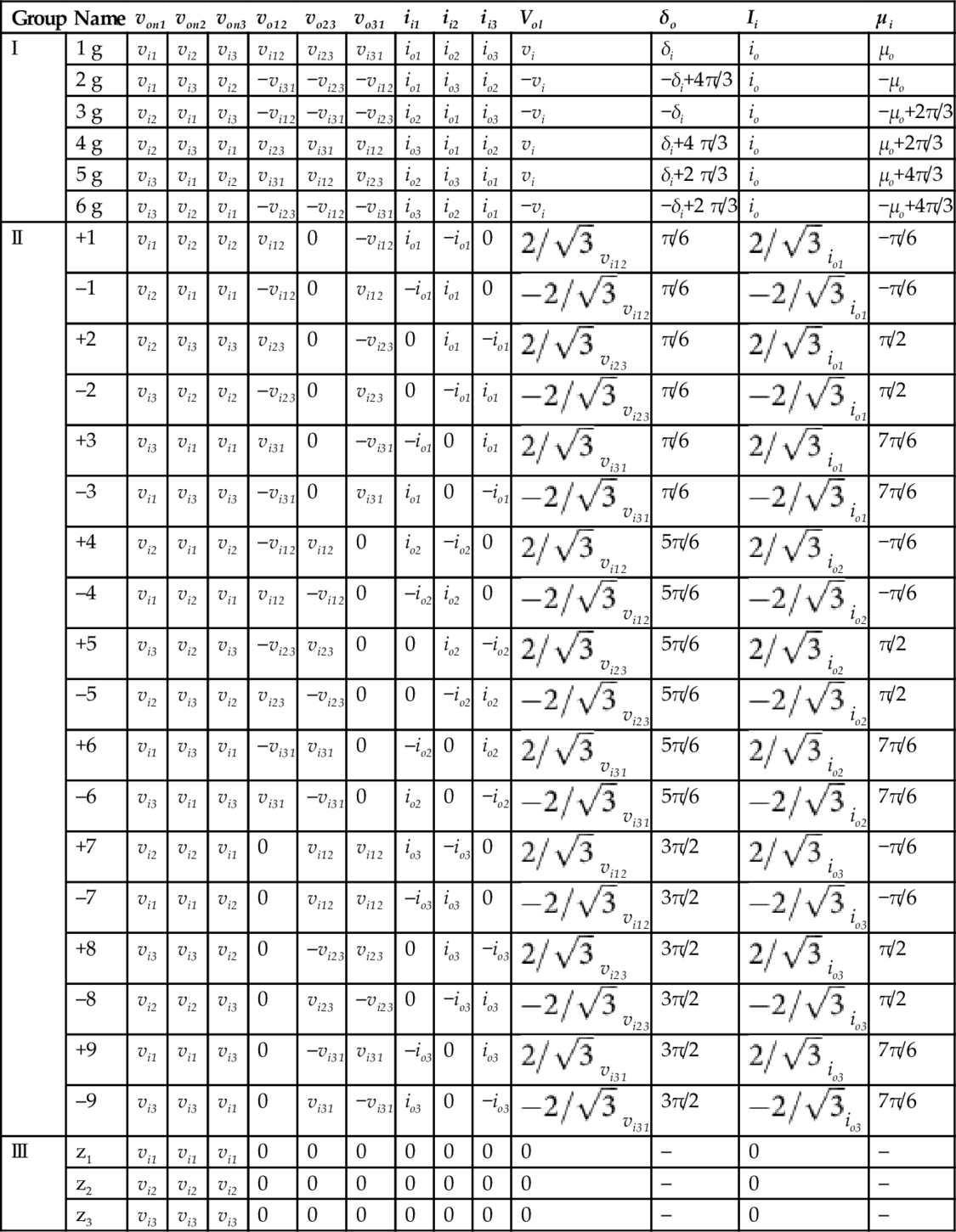
Table 35.6
Switching combinations and output line voltage/input current state-space vectors
| Group | Name | von1 | von2 | von3 | vo12 | vo23 | vo31 | ii1 | ii2 | ii3 | Vol | δo | Ii | μi |
| I | 1 g | vi1 | vi2 | vi3 | vi12 | vi23 | vi31 | io1 | io2 | io3 | vi | δi | io | μo |
| 2 g | vi1 | vi3 | vi2 | −vi31 | −vi23 | −vi12 | io1 | io3 | io2 | −vi | −δi+4π/3 | io | −μo | |
| 3 g | vi2 | vi1 | vi3 | –vi12 | –vi31 | –vi23 | io2 | io1 | io3 | −vi | −δi | io | −μo+2π/3 | |
| 4 g | vi2 | vi3 | vi1 | vi23 | vi31 | vi12 | io3 | io1 | io2 | vi | δi+4 π/3 | io | μo+2π/3 | |
| 5 g | vi3 | vi1 | vi2 | vi31 | vi12 | vi23 | io2 | io3 | io1 | vi | δi+2 π/3 | io | μo+4π/3 | |
| 6 g | vi3 | vi2 | vi1 | –vi23 | –vi12 | –vi31 | io3 | io2 | io1 | −vi | −δi+2 π/3 | io | −μo+4π/3 | |
| II | +1 | vi1 | vi2 | vi2 | vi12 | 0 | –vi12 | io1 | −io1 | 0 | 2/√3 | π/6 | 2/√3 | −π/6 |
| –1 | vi2 | vi1 | vi1 | –vi12 | 0 | vi12 | –io1 | io1 | 0 | −2/√3 | π/6 | −2/√3 | −π/6 | |
| +2 | vi2 | vi3 | vi3 | vi23 | 0 | –vi23 | 0 | io1 | −io1 | 2/√3 | π/6 | 2/√3 | π/2 | |
| –2 | vi3 | vi2 | vi2 | –vi23 | 0 | vi23 | 0 | −io1 | io1 | −2/√3 | π/6 | −2/√3 | π/2 | |
| +3 | vi3 | vi1 | vi1 | vi31 | 0 | –vi31 | –io1 | 0 | io1 | 2/√3 | π/6 | 2/√3 | 7π/6 | |
| –3 | vi1 | vi3 | vi3 | –vi31 | 0 | vi31 | io1 | 0 | −io1 | −2/√3 | π/6 | −2/√3 | 7π/6 | |
| +4 | vi2 | vi1 | vi2 | –vi12 | vi12 | 0 | io2 | −io2 | 0 | 2/√3 | 5π/6 | 2/√3 | −π/6 | |
| –4 | vi1 | vi2 | vi1 | vi12 | –vi12 | 0 | –io2 | io2 | 0 | −2/√3 | 5π/6 | −2/√3 | −π/6 | |
| +5 | vi3 | vi2 | vi3 | –vi23 | vi23 | 0 | 0 | io2 | −io2 | 2/√3 | 5π/6 | 2/√3 | π/2 | |
| –5 | vi2 | vi3 | vi2 | vi23 | –vi23 | 0 | 0 | −io2 | io2 | −2/√3 | 5π/6 | −2/√3 | π/2 | |
| +6 | vi1 | vi3 | vi1 | –vi31 | vi31 | 0 | –io2 | 0 | io2 | 2/√3 | 5π/6 | 2/√3 | 7π/6 | |
| –6 | vi3 | vi1 | vi3 | vi31 | –vi31 | 0 | io2 | 0 | −io2 | −2/√3 | 5π/6 | −2/√3 | 7π/6 | |
| +7 | vi2 | vi2 | vi1 | 0 | vi12 | vi12 | io3 | −io3 | 0 | 2/√3 | 3π/2 | 2/√3 | −π/6 | |
| –7 | vi1 | vi1 | vi2 | 0 | vi12 | vi12 | –io3 | io3 | 0 | −2/√3 | 3π/2 | −2/√3 | −π/6 | |
| +8 | vi3 | vi3 | vi2 | 0 | –vi23 | vi23 | 0 | io3 | −io3 | 2/√3 | 3π/2 | 2/√3 | π/2 | |
| –8 | vi2 | vi2 | vi3 | 0 | vi23 | –vi23 | 0 | −io3 | io3 | −2/√3 | 3π/2 | −2/√3 | π/2 | |
| +9 | vi1 | vi1 | vi3 | 0 | –vi31 | vi31 | –io3 | 0 | io3 | 2/√3 | 3π/2 | 2/√3 | 7π/6 | |
| –9 | vi3 | vi3 | vi1 | 0 | vi31 | −vi31 | io3 | 0 | −io3 | −2/√3 | 3π/2 | −2/√3 | 7π/6 | |
| III | z1 | vi1 | vi1 | vi1 | 0 | 0 | 0 | 0 | 0 | 0 | 0 | – | 0 | – |
| z2 | vi2 | vi2 | vi2 | 0 | 0 | 0 | 0 | 0 | 0 | 0 | – | 0 | – | |
| z3 | vi3 | vi3 | vi3 | 0 | 0 | 0 | 0 | 0 | 0 | 0 | – | 0 | – |
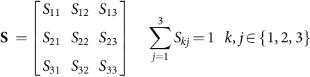
S=[S11S12S13S21S22S23S31S32S33]3∑j=1Skj=1k,j∈{1,2,3}
Based on matrix S, output voltages related to input neutral von1![]() , von2
, von2![]() , and von3
, and von3![]() and line voltages vo12
and line voltages vo12![]() , vo23
, vo23![]() , and vo31
, and vo31![]() can be expressed in terms of matrix converter input phase voltages vi1
can be expressed in terms of matrix converter input phase voltages vi1![]() , vi2
, vi2![]() , and vi3
, and vi3![]() . Input currents ii1
. Input currents ii1![]() , ii2
, ii2![]() , and ii3
, and ii3![]() can be expressed as a function of output currents io1
can be expressed as a function of output currents io1![]() , io2
, io2![]() , and io3
, and io3![]() :
:
[von1von2von3]=S[vi1vi2vi3][vo12vo23vo31]=[S11−S21S12−S22S13−S23S21−S31S22−S32S23−S33S31−S11S32−S12S33−S13][vi1vi2vi3][ii1ii2ii3]=ST[io1io2io3]
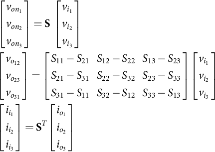
The application of Concordia transformation [Xα,β,0]T=CT [X1,2,3]T to the output line-to-line voltages of Eq. (35.172) results in the output voltage vector:
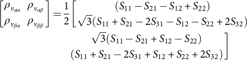
volαβ=[volαvolβ]=√23[1−12−120√32−√32][S11−S21S12−S22S13−S23S21−S31S22−S32S23−S33S31−S11S32−S12S33−S13][vi1vi2vi3]=[ρvααρvαβρvβαρvββ][vicαvicβ]

where vicαβ is the input filter capacitor voltage and ρvαα![]() , ρvαβ
, ρvαβ![]() , ρvβα
, ρvβα![]() , and ρvββ
, and ρvββ![]() are functions of the ON/OFF state of the nine Skj switches:
are functions of the ON/OFF state of the nine Skj switches:
[ρvααρvαβρvβαρvββ]=12[(S11−S21−S12+S22)√3(S11+S21−2S31−S12−S22+2S32)√3(S11−S21+S12−S22)(S11+S21−2S31+S12+S22+2S32)]
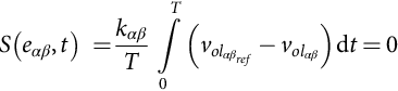
The average value ¯volαβ![]() of the output line-to-line voltages, in αβ coordinates, during one switching period, is the output variable to be controlled (since volαβ is discontinuous) [23,50]:
of the output line-to-line voltages, in αβ coordinates, during one switching period, is the output variable to be controlled (since volαβ is discontinuous) [23,50]:
¯volαβ=1Ts(n+1)Ts∫nTsvolαβdt

Considering the control goal ¯volαβ=¯volαβref![]() , the sliding surface S(eαβ, t)(kαβ>0) is
, the sliding surface S(eαβ, t)(kαβ>0) is
S(eαβ,t)=kαβTT∫0(volαβref−volαβ)dt=0
The first derivative of Eq. (35.176) is
˙S(eαβ,t)=kα(volαβref−volαβ)
As the sliding-mode stability is guaranteed if Sαβ(eαβ, t) ˙Sαβ(eαβ,t)<0![]() , the criterion to choose the output line voltages state-space vectors is
, the criterion to choose the output line voltages state-space vectors is
Sαβ(eαβ,t)<0⇒˙Sαβ(eαβ,t)>0⇒volαβ<volαβrefSαβ(eαβ,t)>0⇒˙Sαβ(eαβ,t)<0⇒volαβ>volαβref

This implies that the sliding mode is reached only when the vector applied to the converter has the desired amplitude and phase.
According to Table 35.6, the six vectors of group I have fixed amplitude but time-varying phase, the 18 vectors of group II have variable amplitude, and the vectors of group III are null. Therefore, from the load viewpoint, the 18 highest amplitude vectors (6 vectors from group I and 12 vectors from group II) and one null vector are suitable to guarantee the sliding-mode stability.
Therefore, if two three-level comparators (Cαβ∈{−1, 0, 1}) are used to quantize the deviations of Eq. (35.178) from zero, the nine output voltage error combinations (33) are not enough to guarantee the choice of all the 19 available vectors. The extra vectors may be used to control the input power factor. As an example, if the output voltage error is quantized as Cα=1 and Cβ=1, at sector Vi1 (Fig. 35.65), the vectors −3, +1, or 1 g might be used to control the output voltage. The final choice would depend on the input current error.

Output current control
For some applications, it is more useful to control the output currents, which implies some changes on the previously designed controllers. From Fig. 35.64, the output currents can be obtained as a function of the phase voltages applied to the load:
{dioαdt=−RLioα+1Lvoα+1LEαdioβdt=−RLioβ+1Lvoβ+1LEβ
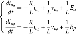
As the output currents are state variables, with a strong relative degree of 1, the sliding surfaces should depend directly on their errors:
Sioαβ(eioαβ,t)=kio(ioαβref−ioαβ)
The state-space vectors should be chosen to guarantee the stability criterion Sioαβ(eioαβ,t)˙Sioαβ(eioαβ,t)<0![]() , according to the following:
, according to the following:
(a) If Sioαβ(eioαβ,t)<0![]() , then ioαβ>ioαβref
, then ioαβ>ioαβref![]() and the output current must decrease ioαβ↓
and the output current must decrease ioαβ↓![]() . This means that the chosen output voltage voαβ
. This means that the chosen output voltage voαβ![]() phase vector should be low enough to guarantee dioαβ/dt<0
phase vector should be low enough to guarantee dioαβ/dt<0![]() .
.
(b) If Sioαβ(eioαβ,t)>0![]() , then ioαβ<ioαβref
, then ioαβ<ioαβref![]() and the output current must increase ioαβ↑
and the output current must increase ioαβ↑![]() . This means that the chosen output voltage voαβ
. This means that the chosen output voltage voαβ![]() phase vector should be high enough to guarantee dioαβ/dt>0
phase vector should be high enough to guarantee dioαβ/dt>0![]() .
.
The output voltage phase vectors can be obtained from the output voltage line vectors of Table 35.6, using the well-known relations between three-phase line and phase voltages:
Vo=[vo1vo2vo3]T=[2vo12+vo2332vo23+vo3132vo31+vo123]T
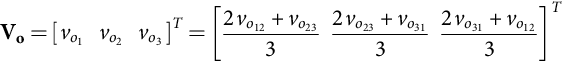
As expected, the resultant output voltage phase vectors will have an amplitude √3![]() lower than the voltage line vectors of Table 35.6 and a lagging phase of π/6. As an example, from Fig. 35.65B, this will result in a −π/6
lower than the voltage line vectors of Table 35.6 and a lagging phase of π/6. As an example, from Fig. 35.65B, this will result in a −π/6![]() rotation of all the voltage vectors represented.
rotation of all the voltage vectors represented.
Therefore, if two three-level comparators (Cαβ∈{−1,0,1}) are used to quantize the deviations of Eq. (35.180) from zero and if the output current error is quantized as Cα=1 and Cβ=1, at sector Vi1 (Fig. 35.65), the vectors +9 or −7 might be used to control the output current. The final choice would depend on the input current error.
Input power factor control
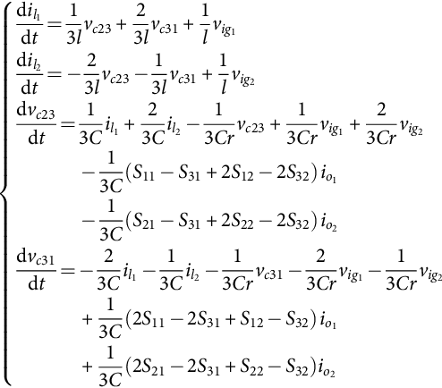
Assuming that the source is a balanced sinusoidal three-phase voltage supply with frequency ωi, the switched state-space model equations of the converter input filter are obtained in 123 coordinates:
{dil1dt=13lvc23+23lvc31+1lvig1dil2dt=−23lvc23−13lvc31+1lvig2dvc23dt=13Cil1+23Cil2−13Crvc23+13Crvig1+23Crvig2−13C(S11−S31+2S12−2S32)io1−13C(S21−S31+2S22−2S32)io2dvc31dt=−23Cil1−13Cil2−13Crvc31−23Crvig1−13Crvig2+13C(2S11−2S31+S12−S32)io1+13C(2S21−2S31+S22−S32)io2
To control the input power factor, a reference frame synchronous with input voltage vig1 may be used applying the Blondel-Park transformation to the matrix converter switched state-space model (Eq. (35.183)), where ρidd![]() , ρidq
, ρidq![]() , ρiqd
, ρiqd![]() , and ρiqq
, and ρiqq![]() are functions of the on/off states of the nine Skj switches:
are functions of the on/off states of the nine Skj switches:
{dilddt=ωiilq−12lvcd−12√3lvcq+1lvigddilqdt=−ωiild+12√3lvcd−12lvcq+1lvigqdvcddt=12Cild−12√3Cilq−13Crvcd+ωivcq+−ρidd+(ρiqd/√3)2Ciod+−ρidq+(ρiqq/√3)2Cioq+12Crvigd−12√3Crvigqdvcqdt=12√3Cild+12Cilq−ωivcd−13Crvcq+−(ρidd/√3)−ρiqd2Ciod+−(ρidq/√3)−ρiqq2Cioq+12√3Crvigd+12Crvigq

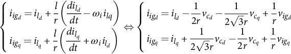
As a consequence, neglecting ripples, all the input variables become time invariant, allowing a better understanding of the sliding-mode controller design, and the choice of the most adequate state-space vector. Using this state-space model, the input iigd and iigq currents are
{iigd=ild+lr(dilddt−ωiilq)iigq=ilq+lr(dilqdt+ωiild)⇔{iigd=ild−12rvcd−12√3rvcq+1rvigdiigq=ilq+12√3rvcd−12rvcq+1rvigq
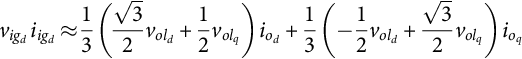
The input power factor controller should consider the input-output power constraint (Eq. (35.185)) (the converter losses and ripples are neglected), obtained as a function of the input and output voltages and currents (the input voltage vigq is equal to zero in the chosen dq rotating frame). The choice of one output voltage vector automatically defines the instantaneous value of the input iigd(t) current:
vigdiigd≈13(√32vold+12volq)iod+13(−12vold+√32volq)ioq
Therefore, only the sliding surface associated to the iigq current is needed, expressed as a function of the system state variables and based on the state-space model determined in Eq. (35.183):
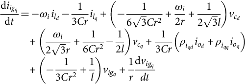
diigqdt=−ωiild−13Crilq+(−16√3Cr2+ωi2r+12√3l)vcd+(ωi2√3r+16Cr2−12l)vcq+13Cr(ρiqdiod+ρiqqioq)+(−13Cr2+1l)vigq+1rdvigqdt
As the derivative of the input iigq(t) current depends directly on the control variables ρiqd![]() and ρiqq
and ρiqq![]() , the sliding function Siq(eiq,t)
, the sliding function Siq(eiq,t)![]() will depend only on the input current error eiq=iigqref−iigq
will depend only on the input current error eiq=iigqref−iigq![]() :
:
Siq(eiq,t)=kiq(iigqref−iigq)
As the sliding-mode stability is guaranteed if Siq(eiq,t)•Siq(eiq,t)<0![]() , the criterion to choose the state-space vectors is [23]
, the criterion to choose the state-space vectors is [23]
Siq(eiq,t)>0⇒˙Siq(eiq,t)<0⇒diigqdt>diigqrefdt⇒iigq↑Siq(eiq,t)<0⇒˙Siq(eiq,t)>0⇒diigqdt<diigqrefdt⇒iigq↓

Also, to choose the adequate input current vector, it is necessary (a) to know the location of the output currents, as the input currents depend on the output currents location (Table 35.6), and (b) to know the dq frame location. As in the chosen frame (synchronous with the vig1 input voltage), the dq-axis location depends on the vig1 input voltage location; the sign of the input current vector iigq component can be determined knowing the location of the input voltages and the location of the output currents (Fig. 35.66).
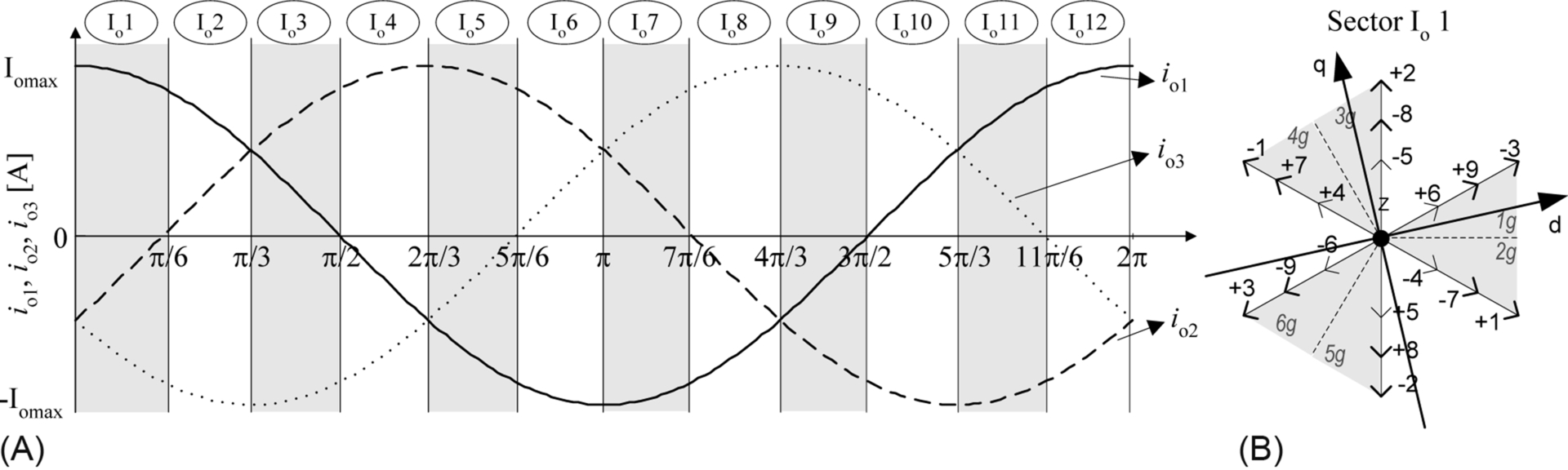
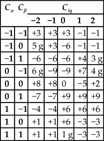
Considering the previous example, at sector Vi1 (Fig. 35.65), for an error of Cα=1 and Cβ=1, vector −3, +1, or 1 g might be used to control the output voltage. When compared, at sector Io1 (Fig. 35.66B), these three vectors have positive id components and, as a result, will have a similar effect on the input iigd current. However, they have a different effect on the iigq current: Vector −3 has a positive iiq component, vector +1 has a negative iiq component, and vector 1 g has a nearly zero iiq component. As a result, if the output voltage errors are Cα=1 and Cβ=1, at sectors Vi1 and Io1, vector −3 should be chosen if the input current error is quantized as Ciq=1 (Fig. 35.66B), vector +1 should be chosen if the input current error is quantized as Ciq=−1, and if the input current error is Ciq=0, vector 1 g or −3 might be used.
When the output voltage errors are quantized as zero Cαβ=0, the null vectors of group III should be used only if the input current error is Ciq=0. Otherwise (being Ciq≠0![]() ), the lowest amplitude voltage vectors ({+2, −8, +5, −2, +8, −5} at sector Vi1 of Fig. 35.65B) that were not used to control the output voltages might be chosen to control the input iigq current as these vectors may have a strong influence on the input iigq current component (Fig. 35.66B).
), the lowest amplitude voltage vectors ({+2, −8, +5, −2, +8, −5} at sector Vi1 of Fig. 35.65B) that were not used to control the output voltages might be chosen to control the input iigq current as these vectors may have a strong influence on the input iigq current component (Fig. 35.66B).
To choose one of these six vectors, only the vectors located as near as possible to the output voltages sector (Fig. 35.67) are chosen (to minimize the output voltage ripple), and a five-level comparator is enough. As a result, there will be 9×5=45 error combinations to select 27 space vectors. Therefore, the same vector may have to be used for more than one error combination.
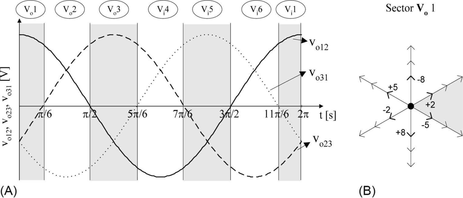
With this reasoning, it is possible to obtain Table 35.7 for sector Vi1, Io1, and Vo1 and generalize it for all the other sectors.
Table 35.7
State-space vector choice at sector Vi1, Io1, and Vo1
| Cα | Cβ | Ciq | ||||
| −2 | −1 | 0 | 1 | 2 | ||
| −1 | −1 | +3 | +3 | +3 | −1 | −1 |
| −1 | 0 | 5 g | +3 | −6 | −1 | −1 |
| −1 | 1 | −6 | −6 | −6 | +4 | 3 g |
| 0 | −1 | 6 g | −9 | −9 | +7 | 4 g |
| 0 | 0 | +8 | +8 | 0 | −5 | +2 |
| 0 | 1 | −7 | −7 | +9 | +9 | +9 |
| 1 | −1 | −4 | −4 | +6 | +6 | +6 |
| 1 | 0 | +1 | +1 | +6 | −3 | −3 |
| 1 | 1 | +1 | +1 | 1 g | −3 | −3 |
The experimental results shown in (Fig. 35.68) were obtained with a low-power prototype (1 kW), with two three-level comparators and one five-level comparator. The transistors IGBT were switched at frequencies near 10 kHz.

The results show the response to a step on the output voltage reference (Fig. 35.68A) and on the input reference current (Fig. 35.68B), for a three-phase output load (R=7 Ω and L=15 mH), with kαβ=100 and kiq=2. It can be seen that the matrix converter may operate with a near unity input power factor (Fig. 35.68A – fo=20 Hz) or with lead/lag power factor (Fig. 35.68B), guaranteeing very low ripple on the output currents, a good tracking capability and fast transient response times.
Also, some simulation results were obtained for the output current-controlled matrix converter. The results (Fig. 35.69A) show the response to a step on the output current reference at t=0.22 s, a step of the output current frequency at t=0.28 s, and a step at the input iigq![]() current at t=0.34 s, for a three-phase output load (R=3 Ω and L=30 mH), with kioαβ=10 and kiq=2. Again, these results show that matrix converter may operate with lead/lag power factor, guaranteeing very low ripple on the output currents, a good tracking capability and fast transient response times for both input and output currents.
current at t=0.34 s, for a three-phase output load (R=3 Ω and L=30 mH), with kioαβ=10 and kiq=2. Again, these results show that matrix converter may operate with lead/lag power factor, guaranteeing very low ripple on the output currents, a good tracking capability and fast transient response times for both input and output currents.

35.3.5.8 Example 35.18: PI Linear Controllers for Matrix Converters
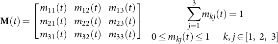
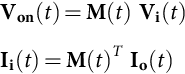
For comparison purposes, a PI-based controller using a pulse-width-modulation (PWM) technique is designed. From Eq (35.171), the modulation indexes mij associated to the matrix converter with nine switches are represented as a nine-element matrix M(t) (Eq. (35.189)) [24]:
M(t)=[m11(t)m12(t)m13(t)m21(t)m22(t)m23(t)m31(t)m32(t)m33(t)]3∑j=1mkj(t)=10≤mkj(t)≤1k,j∈[1,2,3]
These modulation indexes are used to synthesize the output voltages Von(t)=[von1(t)von2(t)von3(t)]T![]() as a function of input voltages Vi(t)=[vi1(t)vi2(t)vi3(t)]T
as a function of input voltages Vi(t)=[vi1(t)vi2(t)vi3(t)]T![]() Eq. (35.190) and input currents Ii(t)=[ii1(t)ii2(t)ii3(t)]T
Eq. (35.190) and input currents Ii(t)=[ii1(t)ii2(t)ii3(t)]T![]() as a function of output load currents Io(t)=[io1(t)io2(t)io3(t)]T
as a function of output load currents Io(t)=[io1(t)io2(t)io3(t)]T![]() Eq. (35.190):
Eq. (35.190):
Von(t)=M(t)Vi(t)Ii(t)=M(t)TIo(t)
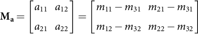
However, assuming a balanced source system 3∑k=1vik(t)=0 with input and output neutral wires not connected 3∑k=1iik(t)=0
 , 3∑k=1iok(t)=0
 , and restriction (35.189), the modulation index matrix may be reduced to a four element akj(t) (k, j={1, 2}) matrix Eq. (35.191) [25]:
Ma=[a11a12a21a22]=[m11−m31m21−m31m12−m32m22−m32]
Based on Eq. (35.189), Eq. (35.190), and Eq. (35.191), input currents are obtained as a function of output currents:
[ii1ii2]T=Ma[io1io2]T
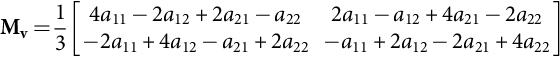
From Eq. (35.189) and Eq. (35.190), output load phase voltages Eq. (35.193) can be directly obtained from input phase voltages using a four modulation index matrix Eq. (35.194) based on Eq. (35.191):
[vo1vo2]T=Mv[vi1vi2]T
Mv=13[4a11−2a12+2a21−a222a11−a12+4a21−2a22−2a11+4a12−a21+2a22−a11+2a12−2a21+4a22]
Assuming ideal input filtering, phase voltages Eq. (35.195) applied to matrix converter should be approximately equal to grid voltages:
vik(t)≈vigk(t)=√2Vicos(ωit−2(k−1)π/3)k∈[1,2,3]
Also, assuming ideal output filtering, output currents Eq. (35.196) should be nearly equal to their fundamental harmonics (with frequency ωo and displacement factor ϕo):
iok(t)=√2Iocos(ωot−φo−2(k−1)π/3)k∈[1,2,3]
If switching frequencies are much higher than input and output frequencies (fs≫fi and fs≫fo), then input currents Eq. (35.197) and output load voltages Eq. (35.198) should be approximately equal to their references:
iik(t)=√2Iicos(ωit−φi−2(k−1)π/3)k∈[1,2,3]
vok(t)=√2Vocos(ωot−2(k−1)π/3)k,j∈[1,2,3]
Applying Concordia and Park transformation [26] to Eq. (35.192) and Eq. (35.193) and choosing a reference frame synchronous with input phase voltages (Θi=ωit![]() ) for all the input variables and a reference frame synchronous with output phase voltages (Θo=ωot
) for all the input variables and a reference frame synchronous with output phase voltages (Θo=ωot![]() ) for all the output variables, then, three-phase input and output variables (Eq. (35.199) and Eq. (35.200)) may become time invariant:
) for all the output variables, then, three-phase input and output variables (Eq. (35.199) and Eq. (35.200)) may become time invariant:
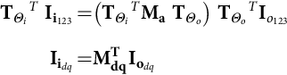
TΘoTVo123=(TΘoTMvTΘi)TΘiTVi123Vodq=MdqVidq
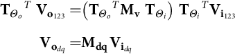
TΘiTIi123=(TΘiTMaTΘo)TΘoTIo123Iidq=MTdqIodq
From Eqs. (35.199) and (35.200), in the new coordinate frame, input phase voltages should be given by Eq. (35.201), and target input currents should be equal to Eq. (35.202):
[vidviq]T=TΘiTViabc=[√3Vi0]T
[iidiiq]T=TΘiTIiabc=√3Ii[cos(φi)−sin(φi)]T
Target output load phase voltages Eq. (35.203) and output currents Eq. (35.204) should be
[vodvoq]T=TΘoTVoabc=[√3Vo0]T
[iodioq]T=TΘoTIoabc=√3Io[cos(φo)−sin(φo)]T
From Eq. (35.199), in the new coordinate frame, matrix converter modulation indexes are given by Eq. (35.205):
Mdq=TΘoTMvTΘi=[γddγdqγqdγqq]

From Eq. (35.199), using input voltages Eq. (35.201), two independent control actions based on different modulation indexes, allowing the independent control of each output voltage component, are obtained:
[vodvoq]T=√3Vi[γddγqd]T
Solving Eq. (35.206) using target output voltages Eq. (35.203), it is possible to calculate γdd Eq. (35.207) and γqd Eq. (35.208) modulation indexes:
γdd=VoVi

γqd=0
Input/output power constraint can be verified Eq. (35.209) by calculating current iid=γddiod+γqdioq![]() from Eq. (35.200) and Eq. (35.205), assuming an ideal matrix converter without losses and input/output ideal filtering, using the previously calculated modulation indexes γdd Eq. (35.207) and γqd Eq. (35.208), input target currents Eq. (35.202) and output currents Eq. (35.204):
from Eq. (35.200) and Eq. (35.205), assuming an ideal matrix converter without losses and input/output ideal filtering, using the previously calculated modulation indexes γdd Eq. (35.207) and γqd Eq. (35.208), input target currents Eq. (35.202) and output currents Eq. (35.204):
ViIicos(φi)=VoIocos(φo)
From Eqs. (35.209) and (35.206), it is possible to conclude the following:
(a) Output voltages (Eq. (35.206)) and input iid![]() current control depend only on γdd and γqd modulation indexes. This shows the well-known nonlinear coupling between output voltages and input currents that results from the input/output active power constraint.
current control depend only on γdd and γqd modulation indexes. This shows the well-known nonlinear coupling between output voltages and input currents that results from the input/output active power constraint.
(b) Output voltages and input iid![]() current are independent from input iiq
current are independent from input iiq![]() current, which depends only on γdq and γqq modulation indexes. This shows that the input power factor is controllable and independent from output voltages control.
current, which depends only on γdq and γqq modulation indexes. This shows that the input power factor is controllable and independent from output voltages control.
From Eqs. (35.200) and (35.205), to guarantee decoupled iid![]() and iiq
and iiq![]() current components, then, γdq and γqq modulation indexes should be given by Eqs. (35.210) and (35.211):
current components, then, γdq and γqq modulation indexes should be given by Eqs. (35.210) and (35.211):
γdq=0
γqq=kγdd
From the previously defined modulation indexes and Eq. (35.200), input iiq![]() current component can be determined by Eq. (35.212):
current component can be determined by Eq. (35.212):
iiq=γqqioq=kγddioq
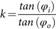
Constant k (Eq. (35.213)) is calculated from Eq. (35.212) using output currents (Eq. (35.204)), target input currents (Eq. (35.202)), and input/output power constraint (Eq. (35.209)):
k=tan(φi)tan(φo)
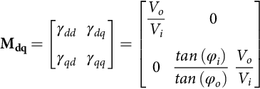
In the previously defined reference frame, the modulation index matrix (Eq. (35.214)) is time invariant and can be obtained from Eqs. (35.207), (35.208), (35.210), (35.211), and (35.213):
Mdq=[γddγdqγqdγqq]=[VoVi00tan(φi)tan(φo)VoVi]
As a conclusion, from Eqs. (35.206) and (35.212), there are three possible control actions:
(a) γdd and γqd to control output currents dq components
(b) k to control input currents power factor
Output current controllers
In order to design the output current controllers, it is assumed that matrix converter is feeding a three-phase general RLE load (Fig. 35.64). In the synchronized dq coordinate frame, output currents are given by Eq. (35.215):
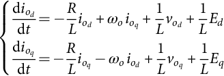
{dioddt=−RLiod+ωoioq+1Lvod+1LEddioqdt=−RLioq−ωoiod+1Lvoq+1LEq
From Eq. (35.215), assuming nearly constant Ed and Eq voltages, Hdq (Eq. (35.216)) command voltages will guarantee that iod![]() and ioq
and ioq![]() output currents follow their references:
output currents follow their references:
{Hd=ωoLioq+vodHq=−ωoLiod+voq
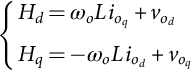
From Eq. (35.206) and Hdq command variables (Eq. (35.216)), matrix converter γdd and γqd modulation indexes (Eq. (35.217)) are calculated as functions of Hdq command voltages, allowing d and q control action decoupling (Fig. 35.70):

{γdd=Hd−ωLioq√3Viγqd=Hq+ωLiod√3Vi

Often, the crossed terms ωLiod![]() and ωLioq
and ωLioq![]() do not have a significant weight and can be neglected.
do not have a significant weight and can be neglected.
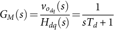
Matrix converter should be defined as having a unitary gain and a dominant pole dependent on the average delay time Td (usually one half of the switching period) [24–27]
GM(s)=vodq(s)Hdq(s)=1sTd+1
The first-order dynamics load may be represented as in Eq. (35.219), where R is the load resistance and τ is the load time constant:
GL(s)=vodq(s)iodq(s)=1R(1+sτ)

Usually, the zero of the compensator is chosen to cancel the pole introduced by the load.
Tz=τ
From Eqs. (35.218) and (35.219) and Fig. 35.70, the closed-loop transfer function is given by
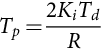
Gcl(s)=KiTpRTds2+s1Td+KiTpRTd

Comparing this transfer function with a second-order system in the canonical form, then, ω2n=Ki/(TpRTd)![]() , where ωn is the natural frequency, and 2ξωn=1/Td
, where ωn is the natural frequency, and 2ξωn=1/Td![]() , where ξ is the damping factor. Choosing ξ=√2/2
, where ξ is the damping factor. Choosing ξ=√2/2![]() to minimize the closed-loop response overshoot and rise time, it is possible to calculate Tp (Eq. (35.222)):
to minimize the closed-loop response overshoot and rise time, it is possible to calculate Tp (Eq. (35.222)):
Tp=2KiTdR
Input current controller
Due to the input/output power constraint (Eq. (35.209)), input iid![]() current depends on the same modulation indexes as output voltages. On the contrary, iiq
current depends on the same modulation indexes as output voltages. On the contrary, iiq![]() is linearly independent from output voltages and iid
is linearly independent from output voltages and iid![]() input current and depends on variable k (Eq. (35.212)):
input current and depends on variable k (Eq. (35.212)):
iiq=γqdiod+γqqioq
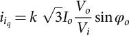
Using the expected values of γqd (Eq. (35.208)) and γdd (Eq. (35.207)) modulation indexes and the target output currents (Eq. (35.204)) in Eq. (35.223), input iiq![]() current is shown to depend linearly on variable k:
current is shown to depend linearly on variable k:
iiq=k√3IoVoVisinφo
Neglecting the input filter dynamics, a nearly unitary matrix converter input power factor is obtained for k=0 and, from Eq. (35.211), for γqq=0![]() . However, as the input filter is not ideal, this will usually result in leading power factor on the grid side connection. To control matrix converter input power factor, a simple integral controller would be enough, as the matrix converter input currents have no associated dynamics, depending directly on the switches states. However, due to the input filter capacitive characteristic, in general, and depending on the operating power conditions, the input power factor on the grid connection will be leading when compared with the controlled matrix converter input power factor.
. However, as the input filter is not ideal, this will usually result in leading power factor on the grid side connection. To control matrix converter input power factor, a simple integral controller would be enough, as the matrix converter input currents have no associated dynamics, depending directly on the switches states. However, due to the input filter capacitive characteristic, in general, and depending on the operating power conditions, the input power factor on the grid connection will be leading when compared with the controlled matrix converter input power factor.
To consider the input filter dynamics in the controller design, it is necessary to relate the grid current iigq![]() to the matrix converter input current iiq
to the matrix converter input current iiq![]() . The resultant second-order transfer function can be further used to design an adequate higher order input current linear controller.
. The resultant second-order transfer function can be further used to design an adequate higher order input current linear controller.
Results
Considering an output three-phase RL load R=3 Ω and L=30 mH, some results were obtained for a step of the output current amplitude at t=0.22 s, a step of the output current frequency at t=0.28 s, and a step of matrix converter input iiq![]() current at t=0.34 s (Fig. 35.71). The input filter dynamics was not considered, and an integral controller was used to control matrix converter input power factor.
current at t=0.34 s (Fig. 35.71). The input filter dynamics was not considered, and an integral controller was used to control matrix converter input power factor.

These results were obtained using the block diagram of Fig. 35.70, assuming that matrix converter model is characterized by Td=1/(2 fm), where fm, the triangular modulator frequency, is fm=10 kHz. They show that the designed controllers guarantee a good response to step changes in the references: The output current io1 and its reference io1ref are almost coincident (Fig. 35.71A), and the matrix converter input current iiq follows its reference value iiqref. As expected, due to the input filter, the grid current is slightly in advance when compared with the iiqref reference current or when compared with matrix converter input current iiq.
35.4 Predictive Optimum Control of Switching Power Converters
35.4.1 Introduction
Predictive optimum controllers are based on linear optimum control systems theory and aim to solve the minimization problem of a cost functional [13,28]. Predictive optimum controllers automatically ensure closed-loop stability and some degree of robustness concerning parameter variation and system disturbances while being easy to numerically implement [13,28].
Predictive controllers can be designed to minimize switching power converter state output errors, together with the switching frequency, being useful to control converter state variables, such as currents, voltages, or powers, even with coupled dynamics. Several approaches to the predictive control of switching power converters are being developed, and obtained results show improvements comparatively to standard modulation techniques or to sliding-mode control [29–38].
35.4.2 Principles of Non-Linear Predictive Optimum Control
The first step in designing a predictive controller is to obtain a detailed nonlinear direct dynamic model (including bounds, saturations, hysteresis, or other effects) of the switching power converter. This model must contain just enough detail for the converter dynamics to allow the model to forecast, in real time and with negligible error, from initial conditions the future behavior of the converter state-space variables and load, over the next sampling steps, with the converter subjected to each possible switching state (or vector).
The next step is to define a cost functional to evaluate the error cost of the application of every vector to the converter. The cost functional contains the weighted control errors and usually is defined as a norm of the error vector and/or weight control efforts, such as the switching frequency.
Known, measured (sampled), or estimated the initial conditions of the state variables, the predictive control algorithm executes by applying every possible control vector to the model. The predicted values of the state-space variables are used to evaluate the controlled output errors corresponding to each one of the available vectors. The errors are weighted, and the value of the cost functional is calculated and stored as a vector.
After applying all the vectors to the model, the minimum of the cost functional vector indicates which switching vector must be applied to the converter in order to nearly zero the output errors in the next sampling step, that is, the next control action of the switching power converter is the vector that obtained the least value of the cost functional. Then, the algorithm is executed again in the next sampling step.
This procedure needs a powerful microprocessor to execute all the predictions in real time using fixed sampling steps (usually within 10–30 ms).
This control technology, here called nonlinear predictive optimum control, is feasible in switching power converters, as they have a reduced set of control actions: from just two in simple dc-dc converters to eight vectors in three-phase PWM inverters or 27 in three-level, three-phase multilevel or matrix converters. Therefore, for these converters, the optimization problem is reduced to the calculation and selection of the vector that generates the minimum value of the cost functional vector. However, for multilevel converters with higher number of levels, the number of vectors steeply increases (125 in five-level three-phase converters). This greatly increases the cost of the control system, since the microprocessor must execute the 125 predictions using a nonlinear model roughly within the same 10–30 ms sampling time. A faster alternative to the predictive optimum controller is also proposed.
35.4.2.1 State and Output Prediction
Consider again the state-space model (35.1), where the input vector has been separated in control vector u and disturbance vector v, being E the disturbance matrix:
˙x=Ax+Bu+Evy=Cx+Du

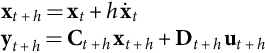
We want to predict the operation of the switching power converter output vector at a future time t+h, yt+h, where h is the predictive controller sampling step. We assume to know both the system state at step t and the system switching vector at step t+h (i.e., we measure the state variables at step t, xt, and know the system matrices at step t+h, At+h, Bt+h, Ct+h, Dt+h, and Et+h, since they depend on a known way from the converter switching vector or they are time invariant). To predict yt+h, we could use the system response obtained from (35.6), substituting the switching period T, by the time difference h between step t+h and step t. For practical converters, Eq. (35.6) must be simplified to minimize calculation time, for example, making eAh≈I+Ah for Ah≪I, which gives the explicit Euler forward method of integration:
xt+h=xt+h˙xtyt+h=Ct+hxt+h+Dt+hut+h
Looking carefully, this prediction method is only a rough approximation, since the switching vector to be applied at t+h is included only in Ct+h and Dt+h, but not in At+h, Bt+h, and Et+h, which are usually strongly dependent on the switching vector applied to the converters. The Euler forward method of integration can be devised to be a first-order truncation of the xt Taylor series expansion in the neighborhood of t:
xt+h=xt+h˙xt+h22!¨xt+h33!˙¨xt+…
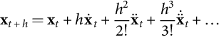
For prediction, the Euler forward is not formally adequate since the future converter switching configuration (vector) is not included explicitly in the predictive equations. Nevertheless, it has been used in predictive control, by using some equation replacement to include the needed converter matrices. Furthermore, the Euler forward method is stable only if the step h obeys h<2/λmax, where λmax is the maximum of the absolute values of all eigenvalues of A. This means that the sampling step must often be too small, which helps to reduce the relative step error (close to h2/4), but increases the needed computing power [29].
The Euler backward is an implicit method derived by backward rewriting a truncated Taylor series as
xt=xt+h−h˙xt+h−…
The unconditionally stable Euler backward algorithm can converge even with long sampling steps, although they are bounded by a relative step error close to−h2/4 [29]:
xt+h=xt+h˙xt+h
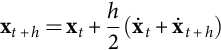
Stable and lower relative step error methods could be used, like the trapezoidal integration method (35.230), but as it needs to calculate both ˙xt![]() and ˙xt+h
and ˙xt+h![]() , it loses the relative step error h3/12 advantage [29] to longer computing times:
, it loses the relative step error h3/12 advantage [29] to longer computing times:
xt+h=xt+h2(˙xt+˙xt+h)
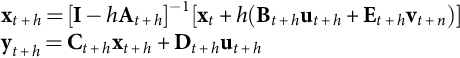
Since we must predict the result of the application of the switching vector at t+h, we should use At+h, Bt+h, and Et+h, for prediction, by selecting the Euler backward method, which gives the system time derivatives at t+h:
˙xt+h=At+hxt+h+Bt+hut+h+Et+hvt+h
Therefore, the converter state variables and outputs at t+h will be
xt+h=[I−hAt+h]−1[xt+h(Bt+hut+h+Et+hvt+n)]yt+h=Ct+hxt+h+Dt+hut+h
This equation means that to predict the converter behavior, the switching vector must define the matrices At+h, Bt+h, Ct+h, Dt+h, and Et+h (or they must be time invariant) and we must measure (or estimate) the state xt, the inputs ut, and disturbances vt to estimate ut+h and vt+h. If ut+h values are based on the switching vectors times dc quantities U, then it might be Ut+h≈Ut, or Ut+h can be estimated using linear extrapolations, such as Euler backward or at least the Euler forward. If vt contains ac sinusoidal voltages, then it should be for ωh≪1:
sin(ω(t+h))=sin(ωt)cos(ωh)+sin(ωh)cos(ωt)≈sin(ωt)+ωhcos(ωt)cos(ω(t+h))=cos(ωt)cos(ωh)−sin(ωt)sin(ωh)≈cos(ωt)−ωhsin(ωt)
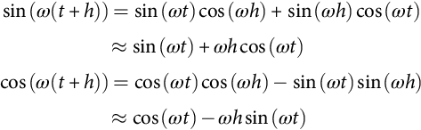
The above equations can also be used to predict the future values of the output vector reference values yref at t+h, if sinusoidal references are being in use and tracking control is sought.
In predictive control, the direct dynamics equations (35.232) are used to predict all the possible future values of the converter outputs, assuming open-loop stability, observability, and all state variables are accessible for measuring or estimation.
35.4.2.2 Minimization of the Cost Functional in Converters with a Reduced Set of Vectors
To solve the minimization problem of the cost functional in a system with a reduced set of m control vectors, consider the errors ej (j∈{1,m}) between the output vector reference values yref and the output at t+h corresponding to the vector j of the control vector set, yjt+h, defined as
ej=yref−yjt+h
Define also Jt+h (35.235) as an m components vector, the quadratic cost functional of the weighted errors ej, and the weighted control action uj, for each control vector j, with weighting matrices ρe and ρu, respectively, for the errors and control actions:
Jt+h=∫∞0(eTjρeej+uTjρuuj)dt
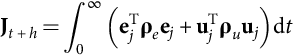
The weighting matrices ρe and ρu are the predictive optimum controller degrees of freedom to penalize excessively high errors or high control efforts, such as high switching frequencies.
After calculating all the m components of the quadratic cost functional Jt+h, the last step in the design of predictive optimum controller is to select the control vector uj to be applied to the converter, as the control vector j for which the quadratic cost functional is minimum:
uj⇔minj[J1t+h,J2t+h,…,Jjt+h,…,Jmt+h]
It is worth to note that the control vector uj just minimizes the defined quadratic cost functional, subjected to the constraints imposed in the converter direct dynamics (35.225). The usual system performance indexes (overshoot, stability margin, disturbance rejection, and robustness) can have little relation with the minimization of the defined quadratic cost functional. This must be considered when defining the cost functional and the weighting matrices of predictive optimum controllers. The designed predictive controller will only perform correctly if, while minimizing the cost functional, it also guarantees adequate steady-state and dynamic behavior. Nevertheless, predictive optimum controllers use state feedback of all the state variables to be controlled and therefore can be tailored to present optimum or near optimum dynamics, considering the physical bounds.
35.4.3 Principles of Non-Linear Fast Predictive Optimum Control
The above algorithm needs to evaluate Eqs (35.232)–(35.235) m times, which can be time-consuming for three-phase multilevel converters with five or more levels.
To reduce the microprocessor computational task, the use of a subset of either adjacent vectors (for minimum switching frequency) or vectors that can zero one or several harmonics, is an alternative to reduce the number of candidate vectors to be analyzed in real time.
Another possibility is to use the converter inverse dynamics to obtain a fast predictive optimum controller, which is here introduced.
From the output equation of the state-space model (35.225), it can be written as
xref=C−1[yref−Dut+h]
Note also that if we suppose that the control objective is attained at sampling time t+h, then xt+h=xref, and from (35.229),
˙xt+h=h−1[xt+h−xt]=h−1[xref−xt]
Using (35.237) in (35.238) and the result in the state equation of (35.225), the converter inverse dynamics, needed to estimate the necessary control vector ut+h, can be obtained:
ut+h=[AC−1D−B−[h−1C−1]D]−1[[A,C−1,−,[h−1C−1],]yref+Ev+[h−1,xt]]
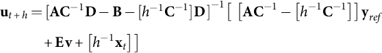
This equation defines the needed components of the control vector ut+h. An alternative way to generate the needed control vector ut+h is to use the controllability canonical form of the converter dynamics to compute the equivalent control, similar to (35.83).
Seldom, the converter will be able to replicate the vector in (35.239), since it is a continuously variable equivalent control vector and the converter only outputs a reduced set of control vectors. Therefore, the control vector ut+h might be either obtained as a kind of space-vector modulation or found by minimization of a quadratic cost functional, based on the norm of the difference vector between the needed ut+h and the available set of vectors uj:
Jjt+h=‖ut+h−uj‖=√(u1t+h−u1j)2+…+(umt+h−umj)2
Then, this functional is computed for all uj, to find the vector that leads to the minimum value of the cost functional (35.240) accordingly to (35.236).
The fast predictive optimum control needs much less computational time, as it only evaluates 35.239 one time per step and (35.240) m times. However, preliminary inspection of Eq. (35.239) indicates that it can only be directly applied to converters with input and output circuits that have time-invariant dynamic matrices.