
EMI Effects of Power Converters
Andrzej M. Trzynadlowski University of Nevada, Reno, NV, United States
Abstract
This chapter is devoted to the effects of electromagnetic interference (EMI) generated by power electronic converters. The switch-mode operation of those converters is explained as a cause of the interference. Measurements of conducted EMI are described, and basic EMI parameters are defined. Common EMI filters and their mathematical models are introduced. Random pulse-width modulation as a means of EMI mitigation is presented. Other means of electromagnetic noise suppression, such as grounding and shielding, are reviewed. Various standards of the electromagnetic compatibility (EMC) are listed along the international institutions issuing those standards. List of useful references and Internet links concludes the chapter.
Keywords
Power electronic converters; Electromagnetic interference; Filters; Random pulse-width modulation; Standards
42.1 Introduction
The term “electromagnetic interference” (EMI) refers to the disturbance in operation of an engineering system due to an electromagnetic impact of the same system or other systems. Conducted electric noise and radiated electromagnetic noise are typical culprits. Watching TV during work hours in industrial centers of Western Europe in the late 1960s was virtually impossible, due to operation of large dc drives and inadequate efforts to fight the EMI threat. Today, proliferation of power electronic converters and communication devices makes EMI mitigation as important as ever, because of the high and growing number of both the potential perpetrators and victims of EMI. To ensure electromagnetic compatibility (EMC), various EMI norms have been established. The issue of EMI is closely linked to that of susceptibility of an electronic circuit to external disturbances. Considering a multicircuit system, if each constituent circuit does not emit above-limit EMI and is immune to below-limit EMI, then each circuit is electromagnetically compatible with the system.
The institution historically entrusted with development of international EMC standards is Comité International Special des Perturbations Radioelectriques (CISPR), founded in 1933, and now forming part of International Electrotechnical Commission (IEC). Drawing on CISPR expertise, numerous other international and national organizations issue norms pertaining to various aspects of EMC. Specific EMI limits are set for internal use by individual countries and organizations, such as armed forces or large corporations. Manufacturers of electric apparatus and systems must comply with the EMC standards to have an access to the market.
In this chapter, EMI effects of power electronic converters are illustrated, and basic terms and units are introduced. EMI measurement techniques and preventive measures are described, and EMC standardization efforts are examined.
42.2 Power Converters as Sources of EMI
The switch-mode operation of power electronic converters results in rippled currents. Also, rapid changes of the switched voltages induce currents in parasitic (stray) capacitances that couple the converter with other closely spaced circuits. Distorted currents drawn from the power grid produce distorted voltage drops generating pervasive voltage noise. In general, the voltage disturbances can be divided into three classes: (1) noise, (2) short-duration impulses superimposed on the mains voltage, and (3) transients.
Electromagnetic disturbances travel by conduction on wiring (conducted EMI), radiation in space (radiated EMI), and intercircuit capacitive or inductive coupling. Below 10 MHz, the EMI spreads mainly by conduction, whereas at higher frequencies mostly by radiation. The frequency range of 0.15–30 MHz occupies an important place in EMC norms because it covers the radio and TV broadcast. According to those norms, in that range, it is the conducted EMI that must be measured and suppressed, whereas measurements of the radiated EMI are required only under special circumstances. Power electronic equipment typically produces EMI that is broadband and contained within a frequency range from the operating frequency to several megahertz. Recently, the very low-frequency range of 10–150 kHz has been receiving an increased attention. Consequently, with respect to most power electronic converters, it is the conducted EMI that is considered a major nuisance.
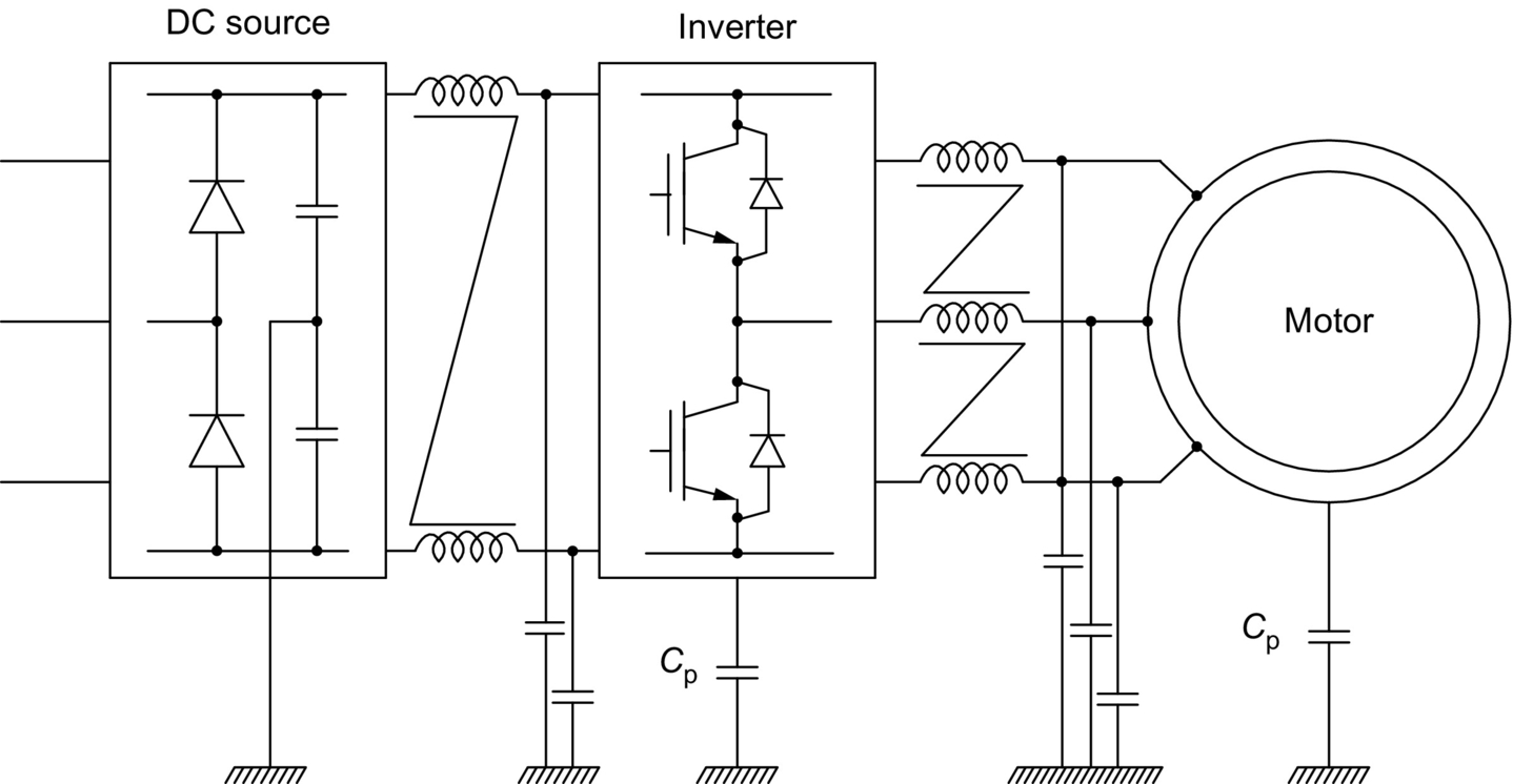
Conducted EMI appears in the form of common-mode (CM) and differential-mode (DM) voltages and currents. These two modes are illustrated in Fig. 42.1, which depicts an adjustable-speed ac drive with a PWM voltage-source inverter. CM currents, icm, flow to the ground through parasitic capacitances, Cp, whereas DM currents, idm, flow only in the wires of the system. Considering the two-wire dc line supplying the inverter, the rms CM voltage, Vcm(2), is defined as
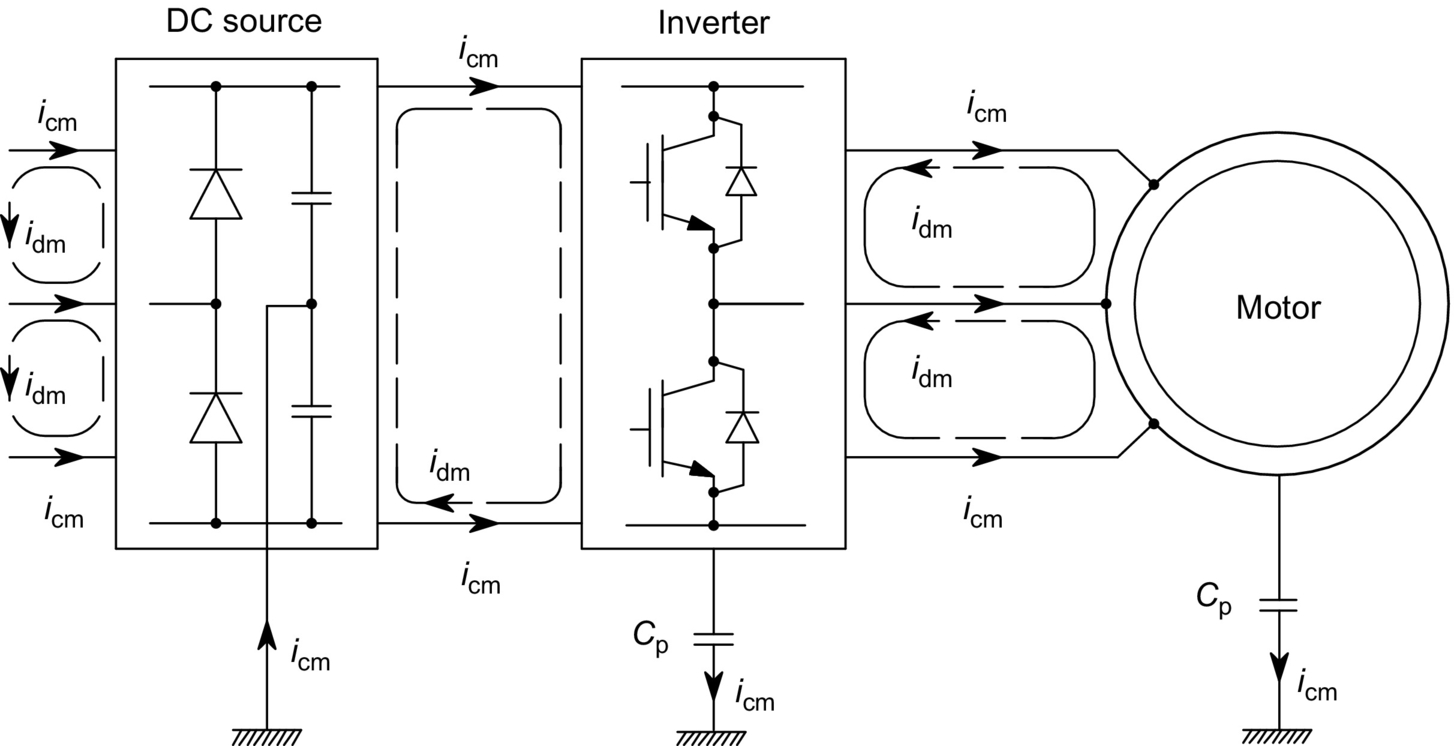
and the rms DM voltage, Vdm(2), as
where V1 and V2 are line-to-ground voltages of the two wires. The rms CM and DM currents, Icm(2) and Idm(2), are defined as
For the three-wire supply and load ac lines, the rms CM voltage, Vcm(3), and current, Icm(3), are defined as

where subscript “3” applies to the third wire. The DM voltage and current, if measured with respect to ac wires 1 and 2, are defined by Eqs. (42.2) and (42.4) as for the two-wire system.
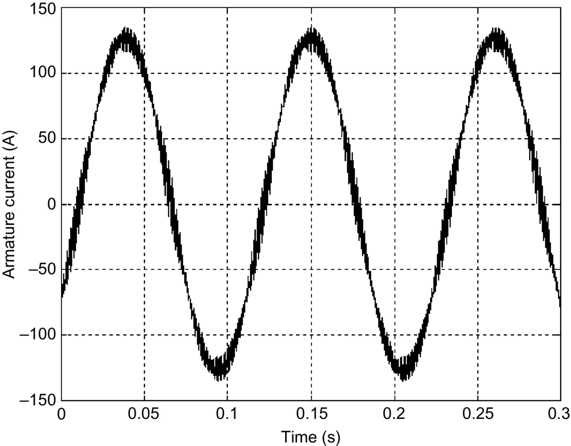
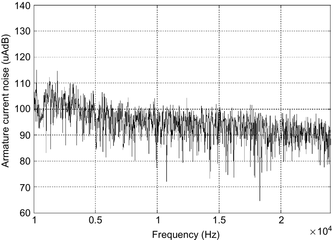
To illustrate EMI generation by PWM power converters, a typical waveform of output current of the inverter in Fig. 42.1 is shown in Fig. 42.2. The fundamental sine wave dominates, but the high-frequency current ripple is also observable. As seen in Fig. 42.3, numerous clusters of higher harmonics appear in the frequency spectrum of the current. Their locations coincide with multiples of the switching frequency (here 2 kHz), which, as in all PWM converters, is much higher than the fundamental frequency (here 9 Hz) of the ac output (or input) voltage.
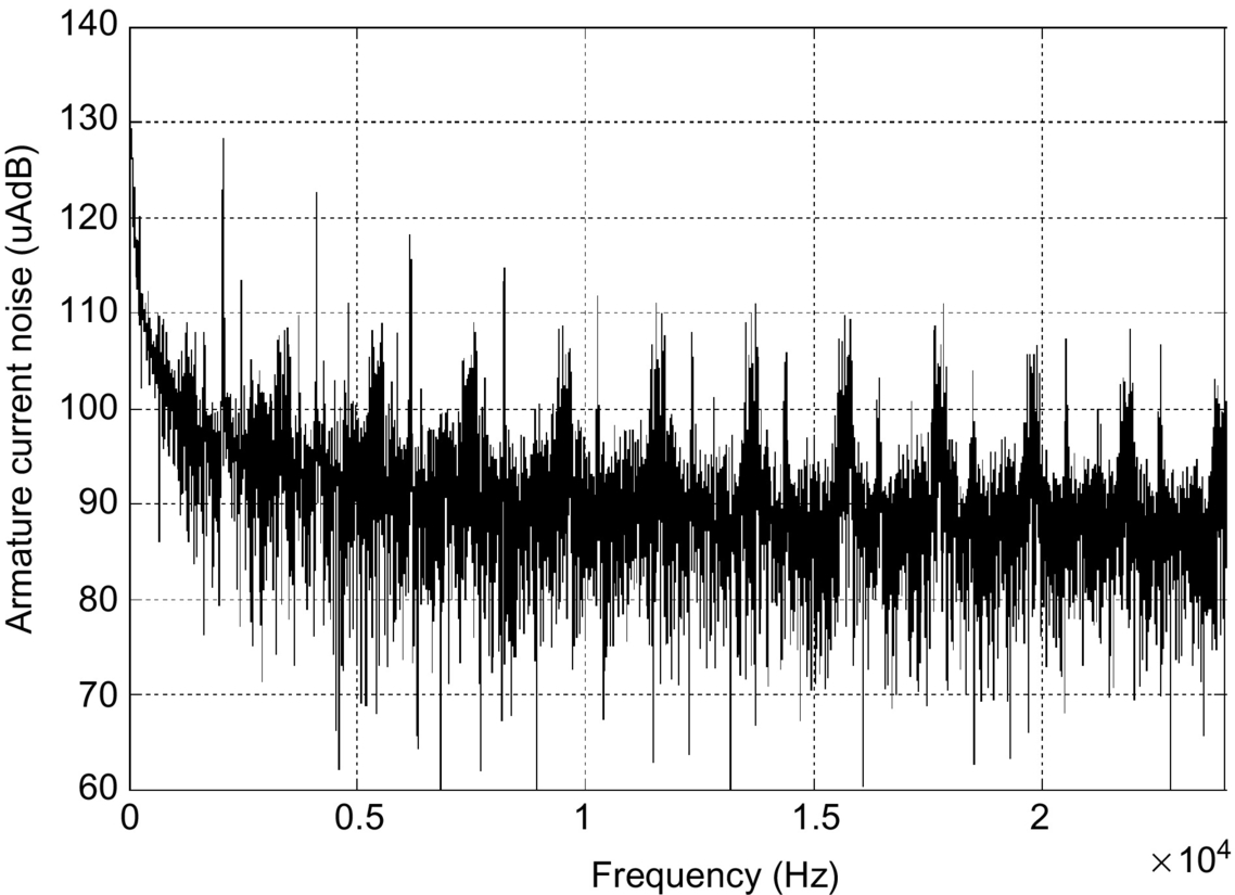
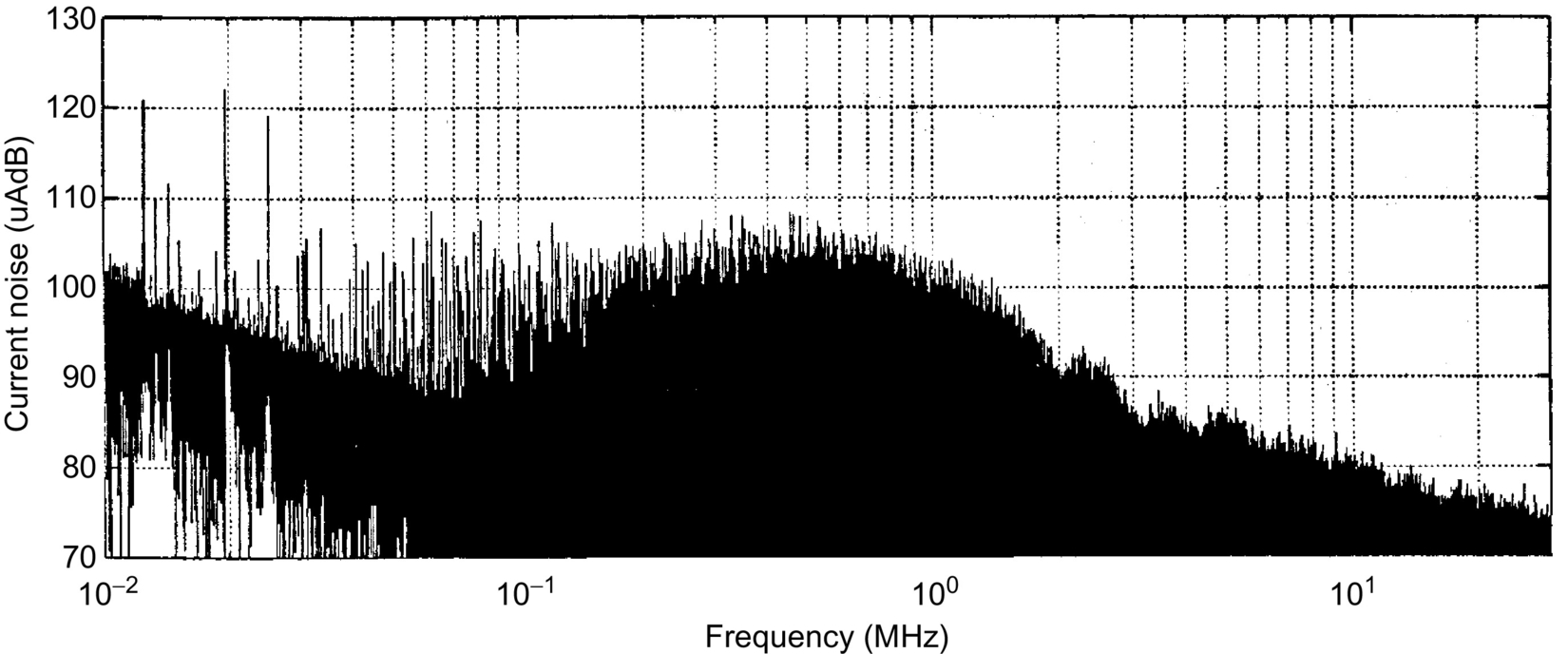
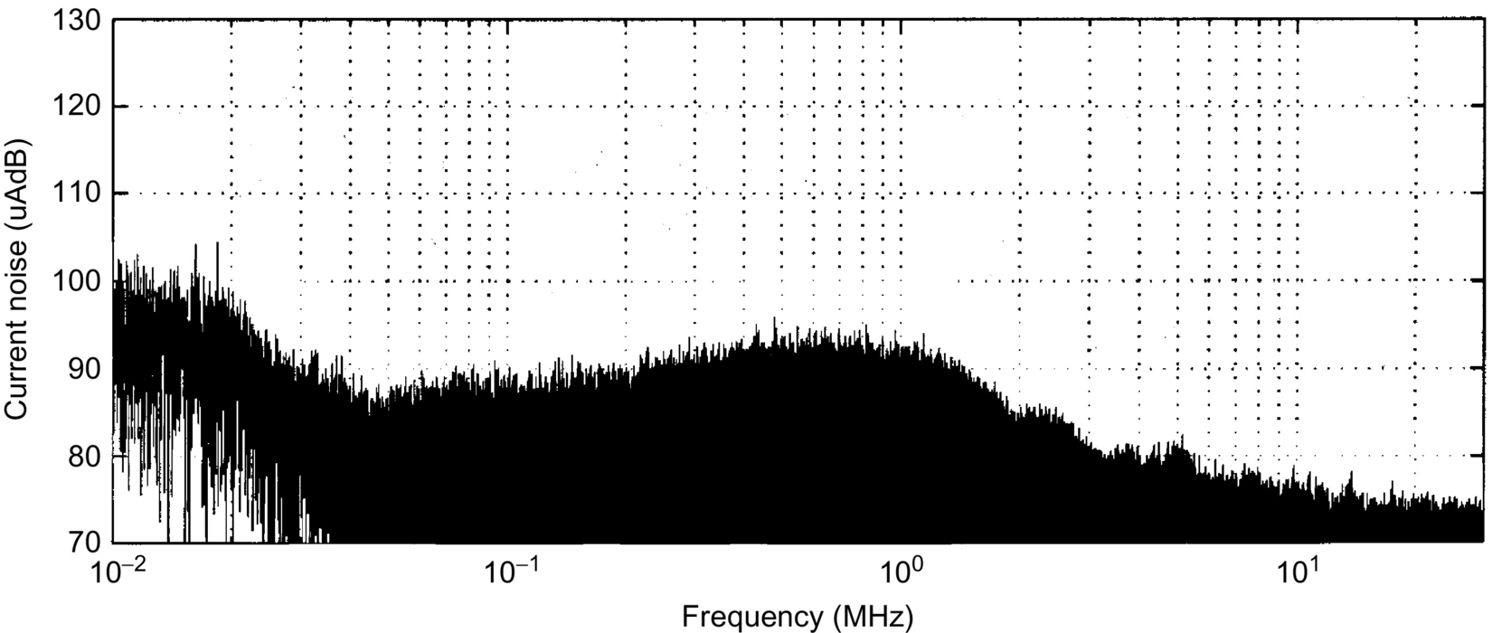
The range of frequency in Fig. 42.3 is narrow (24 kHz). A wide-range frequency spectrum of current of another inverter is shown in Fig. 42.4. It can be seen that the harmonics become progressively less prominent when the frequency increases. This observation justifies the already mentioned focus on the frequencies below 30 MHz.
The fast ON-OFF and OFF-ON state transition of switches, whose switching times are typically in the order of a fraction of microsecond, also causes EMI. It is due to the high dv/dt ratios, which generate transient charge currents in the interwire capacitances of cables, intrawinding capacitances of transformers and p-n junctions of power diodes. Transient circuit-to-ground currents through parasitic capacitances also produce EMI. If not filtered out, the transients appear in current waveforms as spikes on top of the fundamental sinusoid. The circuit-to-ground current spikes constitute CM emissions, whereas the ripple current and periodic current spikes, coincident with the switching pattern of the converter, comprise DM emissions.
Power electronic converters tend to generate current-related interference at their input, injecting noise to the power grid, and voltage-related interference at their outputs. It may disturb operation of communication and control systems in proximity to the converter. Considering the popular low-power dc-to-dc converters, the flyback and buck converters produce particularly noisy input currents because the semiconductor switch is directly in series with the input power line. In conjunction with the finite source impedance, the EMI from dc-to-dc converters conducted by the line can cause disturbance of operation of system operating from a common power bus. Disturbances can also be caused by emissions radiated from converters with very high switching frequencies. The radiated EMI is most often a magnetic field, due to the typically low voltages and high currents involved, but electric fields can sometimes also be a nuisance, especially with respect to the own control circuitry of the converter. Power lines can also radiate EMI produced by the current noise drawn from converters.
42.3 Measurements of Conducted EMI
Mitigation of conducted EMI is of major practical importance in power electronic systems. Therefore, the topic of EMI measurements in this chapter is limited to the 10 kHz–30 MHz frequency range. The related terms, units, instruments, and techniques are subsequently described. Concerning the radiated interference, the reader is referred to one of many publications covering the radio-frequency (RF) aspects of EMC, for example [1–5].
The basic quantity of a signal is power. Because of the potentially wide magnitude ranges involved, the decibel (dB) system is often used in which 1 W serves as the reference. In the dB system, signal power, P(dBW), expressed in dBW, is calculated from the power in watts, P(W), as
If milliwatts, mW, often abbreviated as “m,” is considered; then
However, in EMI measurements, it is voltage that is commonly used, and voltage probes are employed. Power is proportional to the square of voltage. Thus, taking 1 V as reference, voltage in the logarithmic scale, V(dbV), is defined as
In practice, the reference voltage is usually 1 μV, and
If the commonly used resistance of 50 Ω is employed in the measurements, conversions of P(dBm) into V(dBμV) and vice versa can be made from the equation:
Current probes for EMI measurements are used when limits on conducted EMI are expressed in units of current. Denoting the terminal-pair transfer impedance of a current probe by ZT, current expressed in dBμA, is given by
where
To characterize broadband coherent (continuous spectrum) signals, an amplitude density function, A, is used in place of a discrete amplitude measure. The so-called broadband unit is 1 V/Hz. In EMC techniques, the 1 μV/MHz unit is more convenient. The conversion equations are
and
where B(MHz) is the measurement bandwidth, usually 9 kHz, that is, 0.009 MHz.
Conducted emissions are measured using EMI receivers, which usually measure voltage from an appropriate probe. Basically, the EMI receiver is a tunable voltmeter; its block diagram is shown in Fig. 42.5. Modern EMI receivers cover extremely wide frequency ranges, for example, from 9 kHz to 18 GHz.
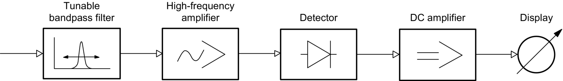
To allow comparison of EMI measurement results, precise specifications for the detector have been established. The most common types are peak, quasi-peak, and average detectors. They are based on RC circuits having different charging and discharging time constants. It must be mentioned that the displays are usually calibrated to the rms value of an equivalent sinusoidal signal, whereas the actual detector often measures a different characteristic of the culprit noise.
Measurement of the peak EMI is important because of the ubiquity of impulsive sources and sensitivity of many types of electronic circuits to impulses. The peak detectors have a short charging time constant, in the order of a fraction of microsecond, and a very long discharging time constant, in the order of tens of seconds. The quasi-peak detectors, strongly recommended by CISPR, have been primarily developed to emulate the human ear acting as a broadcast disturbance sensor. The charging and discharging time constants are 1 and 160 ms, respectively. The average detector is characterized by a long integration time constant, in the order of a second. For the 0.15–30 MHz frequency range, CISPR requires that an EMI measuring instrument have a 9 kHz bandwidth of the filter at 6 dB (from ![]() to
to ![]() kHz from the central frequency value) and that the measurement accuracy for a sinusoidal signal be less than 2 dB.
kHz from the central frequency value) and that the measurement accuracy for a sinusoidal signal be less than 2 dB.
To increase the accuracy within wide ranges of the frequency and magnitude of signals, modern EMI receivers have several measuring channels. Each channel contains an independent quasi-peak detector, and the saturation and threshold levels of individual channels differ from each other. Output signals of the detectors are added in a circuit operating the display.
For comparability of EMI measurements, an interface circuit is inserted between the EMI source and the mains. This circuit is called a line impedance stabilization network (LISN) or artificial mains. The LISN produces a standard load impedance for the EMI source and filters out high-frequency disturbances on the mains, which could distort measurement results. An example of single-phase LISN recommended by CISPR 16—a publication devoted to proper EMI testing—is shown in Fig. 42.6. In the equipment under test (EUT) block, the positive and negative line terminals are denoted by P and N, respectively, whereas grounded terminal is denoted by G. The load resistance, RL, specified by CISPR 16 is 50 Ω. The switch, S, allows transition from the CM to DM measurements. Three-phase LISNs are also available. Refer to the manual of a given LISN for operating instructions.

For quick qualitative EMI measurements, for example, when developing an EMI filter, a spectrum analyzer can be employed. A direct view of the interference levels over a wide frequency range is very convenient. The frequency axis can be switched to a linear or logarithmic scale, whereas the magnitude is usually displayed in dBm. True peak and average detectors are available. Spectrum analyzers are rms calibrated, so that the reading is correct for sinusoidal waveforms only, such as discrete harmonics of the measured noise. For impulse disturbances, correct peak values are obtained. For broadband measurements, corrections must be made to convert the true peak to quasi-peak and to account for the difference in measurement bandwidths. For help, refer to the manual of a given spectrum analyzer.
Technical details of EMI measurements for EMC compliance are too vast, a topic to be fully covered here. The reader is referred to such authoritative sources as the already mentioned CISPR publication 16 and books [1–6].
42.4 EMI Filters
EMI generated in power electronic systems usually exceeds the allowable levels, so it must be reduced. The most common means of EMI mitigation are low-pass filters, often called radio-frequency (RF) filters. They are installed on the input and output sides of power converters. The filters are simple capacitive (C) or inductive-capacitive (LC) circuits. Resistors are sometimes added to dampen possible resonances caused by converters with high switching frequencies.
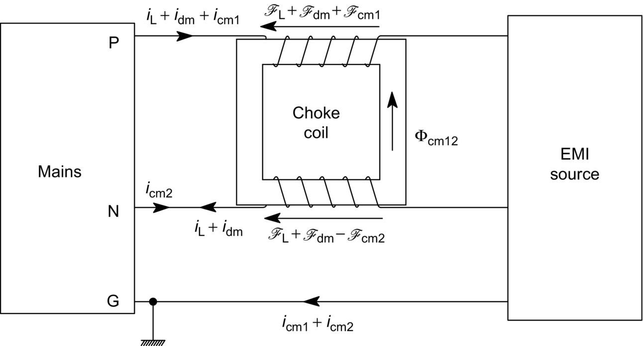
Choke coils are employed as the inductive components of the filters. They are usually single-layer solenoid structures with relatively low coefficients of inductance. In the case of CM EMI filters, two or three windings are placed on the same closed iron core. The windings are so arranged that the coil impedance for the CM noise is high, but that for the load current and DM noise is low. A single-phase CM choke coil is shown in Fig. 42.7. Again, letters P, N, and G denote the positive, negative, and ground terminals of the mains. It can be seen that magnetomotive forces ℱL and ℱdm produced by the load current iL and DM noise current idm in the upper and lower parts of the coil cancel each other. As a result, the magnetic flux Φcm12 in the core is generated only by magnetomotive forces ℱcm1 and ℱcm2 produced by the CM noise currents icm1 and icm2.
Capacitors employed in EMI filters must have low parasitic series inductance, low dielectric and ohmic losses, and stable capacitance versus frequency characteristics. Paper, metalized paper, polystyrene, and ceramic capacitors are widely used. The so-called multifunction ceramic (MFC) capacitors can suppress the high-frequency noise and absorb impulse-type transients. According to their electric connection mode, capacitors in power line filters can be classified as X and Y capacitors, the former posing no threat of electric shock to personnel, even in the case of a breakdown. Y capacitors are typically used for attenuation of the CM noise in power line filters, but they require stricter safety standards and higher reliability than X capacitors.
To reduce the parasitic inductance, contributed mostly by the leads, the so-called feedthrough capacitors have been developed for use in EMI filters. The wire conducting the load current passes through the capacitor structure, instead of the capacitor being connected between it and the ground. This is illustrated in Figs. 42.8 and 42.9. Fig. 42.8A shows the structure of the feedthrough capacitor, and its electric symbol is shown in Fig. 42.8B. Fig. 42.9A shows that in a conventional capacitor, the parasitic inductances, Lp, of the leads are in series with the capacitance, C. The total inductance is thus 2Lp. In contrast, as seen in Fig. 42.9B, in the feedthrough capacitor, lead inductances are connected in parallel to each other, so that the total inductance is Lp/2.


From the very beginning of modern power electronics, capacitors have been employed in the so-called snubbers. In the simplest embodiment, a snubber circuit consists of a capacitor with a resistor connected in series to dampen possible resonance with parasitic inductances. The snubber is placed across a semiconductor power switch to improve the switching conditions and keep the switch within its safe operating area. Snubbers reduce the EMI, which is particularly strong when the switch turns off and interrupts the load current.
Noise suppression capacitors connected to various other points in a power electronic system are also widely used, although they do not mitigate the EMI as effectively as LC filters with choke coils. Capacitive filters most often appear at the input and output of power electronic converters. They can be connected between lines or line to ground.
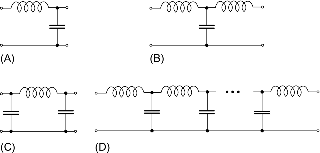
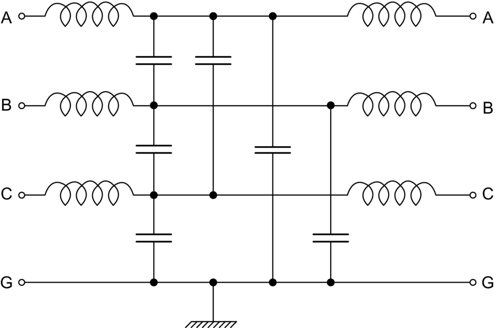
Basic topologies of low-pass LC filters are illustrated in Fig. 42.10. It must be stressed that EMI filters must be placed in all wires of a power electronic system. Most common configurations are shown in Fig. 42.11 for a two-wire system. The filters attenuate both the CM and DM conducted EMI. An extension of the T-type filter on a three-wire system is shown in Fig. 42.12. Similar extension can be made with respect to the other topologies of filters.

An example arrangement of the CM and DM EMI filters in the ac drive system of Fig. 42.1 is shown in Figs. 42.13 and 42.14, respectively. In the actual system, both types of filters are installed, and the two separate circuit diagrams have been used for an instructional purpose only.

The main parameter of EMI filters is the insertion loss (IL). For a given frequency, f, IL can be determined by measuring the voltage, VG, of a sinusoidal signal generator and then connecting the filter to the generator and measuring the voltage, VF, at the filter's output. Then,
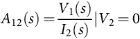
The insertion loss is usually given as an IL(f) graph with logarithmic coordinates. For filter design, the two-port network theory is employed, using the transmission, A, parameters expressing the dynamic relations between the input and output variables of a two-port network. Specifically,
where V1 denotes the input (EMI-source side) voltage of the network, I1 is the input current, V2 is the output voltage, and I2 is the output current, whereas s denotes the Laplace variable (complex frequency). The transmission parameters are defined as

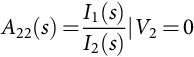
Once the transmission parameters for a given filter are determined using the transient analysis of its circuit, the insertion loss can be found from the following equation:
where ![]() . Then, the IL(f) graph can be plotted, as illustrated in Fig. 42.15 for an actual commercial EMI filter.
. Then, the IL(f) graph can be plotted, as illustrated in Fig. 42.15 for an actual commercial EMI filter.

The insertion loss is approximately proportional to the total inductance and capacitance (total LC) and square of the frequency. Because of the cost and size associated with the total LC value of the filter, an optimal filter is the one with a minimum total LC value, which still mitigates the EMI sufficiently to satisfy the pertaining norm. A difficulty in optimizing the EMI filter design consists in the mismatched impedance conditions under which the filters operate. From the point of view of a manufacturer of the filters, the source and load impedances are unknown. However, from the user's viewpoint, estimating the source and load impedances allows for better selection of the filter configuration. Specifically, for low source and load impedance, the “T” filter is recommended. The “Π” configuration is best for high source and load impedance, whereas for low source and high load impedance, the “Γ′” (LC) filter is preferred. Finally, for high source and low load impedance, the “Γ” (CL) topology is favored. If possible, multiple-stage filter topologies should be employed.
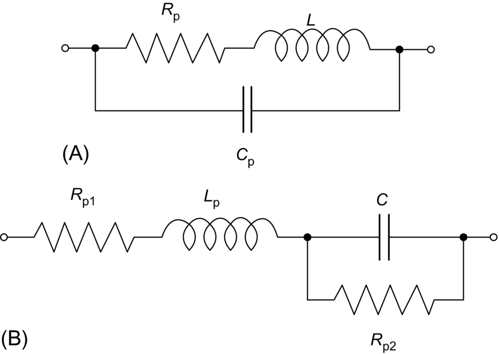
Practical design of EMI filters is complicated by the fact that there are no ideal inductors and capacitors. Considering the equivalent electric circuit of an inductor in Fig. 42.16A and that of a capacitor in Fig. 42.16B, it can be seen that at very high frequencies, the impedance of the parasitic components, marked by the subscript “p,” may dominate that of the main component. Thus, the reactance of the parasitic capacitance, Cp, of the inductor can make the overall impedance to decrease with the frequency, and the reactance of the parasitic inductance, Lp, of the capacitor can make the overall impedance of the capacitor to increase. That is why manufacturers of EMI filters and their components go to great lengths to minimize the parasitics.
In the common case of power electronic converters fed from the grid, the so-called power line filter is installed between the grid and converter. It protects the converter and its load from external disturbances and, vice versa, screens out the grid from EMI generated in the converter. Voltage impulses originated within the grid are particularly hazardous for the converter, and varistors are used in the filter to attenuate the impulses. An example of commercial power line filter is shown in Fig. 42.17. In the drive system in Fig. 42.1, the filter would be connected to the three-phase input terminals of the dc source (rectifier).

Numerous vendors offer a variety of power line and EMI filters with a wide range of voltage and current ratings. Thus, designers of power converters and converter-fed systems have a choice of quality products, without the need for designing their own filters. Useful details of the process of EMI filters design can be found in [7,8].
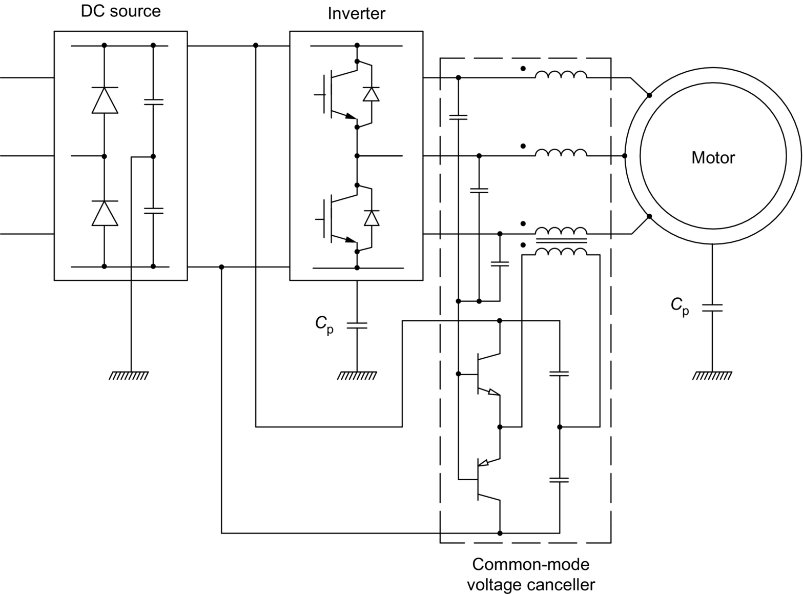
Active EMI filters, although very effective, are less common than the passive filters described because of their increased complexity and cost. They are based on the feedback principle, generating currents that neutralize the noise currents. In the dc-to-dc converters, they are also employed to limit inrush currents, for example, during the so-called hot swapping, when a faulty electronic board is replaced without interrupting operation of the system. In certain three-phase systems with power converters such as ac drives, the CM voltage noise, apart from producing external interference, causes internal problems, for example, accelerated wear of bearings. The so-called CM voltage cancellers are one of the means to mitigate those problems. Such a voltage canceller in the drive system of Fig. 42.1 is shown in Fig. 42.18.
42.5 Random Pulse Width Modulation
Suppression of the low-frequency noise originating from the PWM operating mode of most power converters is particularly difficult. As already pointed out in Section 42.1, the noise, mostly harmonics of the voltages and currents, appears in the frequency spectra as harmonic clusters around multiples of the switching frequency, fsw. As seen in Fig. 42.3, the highest magnitudes of the harmonics appear at the lower end of the frequency range, while the insertion loss of EMI filters progressively increases with the frequency, as shown in Fig. 42.15. Thus, at low frequencies, effectiveness of the filters decreases. Increasing the total LC value helps, but it results in corresponding increase of the cost and bulk of the filters. Therefore, mitigation of harmonics by means of special PWM strategies is the best solution for filter minimization.
Most of the commercial PWM power converters are characterized by a fixed switching frequency, fsw, defined here as a reciprocal of the switching period, Tsw. The switching period constitutes the length of a switching interval, which houses pulses of switching variables of the converter, one pulse per variable. Duty ratio of a given pulse varies from 0 to 1; that is, the width (duration) of the pulse is in the range of ![]() . It has been demonstrated in many publications, for example, [9] that if individual switching periods are randomly varied, then the discrete harmonic power (watts) of spectra of the voltages and currents of the converter is transferred to continuous power spectral density (watts/hertz). This strategy of random pulse-width modulation (RPWM) results in significant mitigation of both the acoustic and electromagnetic noise associated with the current harmonics [10,11]. Accumulated experience and theoretical considerations show that varying Tsw from 0.5 to 1.5 of the average switching period, Tsw,ave, is sufficient. Thus, the nth switching period is determined as
. It has been demonstrated in many publications, for example, [9] that if individual switching periods are randomly varied, then the discrete harmonic power (watts) of spectra of the voltages and currents of the converter is transferred to continuous power spectral density (watts/hertz). This strategy of random pulse-width modulation (RPWM) results in significant mitigation of both the acoustic and electromagnetic noise associated with the current harmonics [10,11]. Accumulated experience and theoretical considerations show that varying Tsw from 0.5 to 1.5 of the average switching period, Tsw,ave, is sufficient. Thus, the nth switching period is determined as
where rn is a uniform-probability random number in the 0–1 range.
For convenience, in practical digital modulators for PWM converters, the switching cycles coincide with the sampling cycles of the modulator, that is, ![]() , where fsmp denotes the sampling frequency (not to be confused with the much higher clock frequency). Consequently, the varying switching rate is associated with identically varying sampling rate. When a single digital system performs more tasks than just PWM, the random sampling rate is a disadvantage. For instance, in a control system, the sampling rate defines the control bandwidth, and it is selected at a specific trade-off level. Therefore, an RPWM technique with a fixed sampling rate but variable switching frequency is more practical. Fig. 42.19 illustrates (A) the most common, nonrandom PWM technique with fixed-period and coinciding sampling and switching cycles; (B) RPWM with randomly varied and coinciding sampling and switching cycles; and (C) RPWM with fixed sampling periods and randomly varied switching periods, subsequently referred to as variable-delay RPWM (VD-RPWM).
, where fsmp denotes the sampling frequency (not to be confused with the much higher clock frequency). Consequently, the varying switching rate is associated with identically varying sampling rate. When a single digital system performs more tasks than just PWM, the random sampling rate is a disadvantage. For instance, in a control system, the sampling rate defines the control bandwidth, and it is selected at a specific trade-off level. Therefore, an RPWM technique with a fixed sampling rate but variable switching frequency is more practical. Fig. 42.19 illustrates (A) the most common, nonrandom PWM technique with fixed-period and coinciding sampling and switching cycles; (B) RPWM with randomly varied and coinciding sampling and switching cycles; and (C) RPWM with fixed sampling periods and randomly varied switching periods, subsequently referred to as variable-delay RPWM (VD-RPWM).

As seen in Fig. 42.19C, the switching cycles in the VD-RPWM method are delayed with respect to the corresponding sampling cycles by a randomly varied time delay, d. The value of d for the nth switching cycle is calculated as
where ![]() denotes the sampling period. When in two consecutive switching cycles, denoted by k and
denotes the sampling period. When in two consecutive switching cycles, denoted by k and ![]() , rk is close to 1, and
, rk is close to 1, and ![]() is close to 0; the second,
is close to 0; the second, ![]() , switching cycle may be too short; that is, its length,
, switching cycle may be too short; that is, its length, ![]() , may be lower than the minimum allowable length, Tsw,min. Therefore, in case of such occurrence,
, may be lower than the minimum allowable length, Tsw,min. Therefore, in case of such occurrence, ![]() is set to Tsw,min, or another value of rk is selected. As a result, the switching periods vary from Tmin to 2Tsmp. The average switching period, Tsw,ave, equals the sampling period, Tsmp.
is set to Tsw,min, or another value of rk is selected. As a result, the switching periods vary from Tmin to 2Tsmp. The average switching period, Tsw,ave, equals the sampling period, Tsmp.
Any PWM strategy based on the concept of switching cycles can be employed within the RPWM method. For instance, the popular space-vector modulation can be used in three-phase voltage-source inverters. As long as the average switching period is sufficiently short, the quality of output current is similar to that in a converter with a fixed switching frequency having the same period. An example spectrum of the output current of a voltage-source inverter controlled using the VD-RPWM is shown in Fig. 42.20. It is the same converter whose current spectrum, with fixed-period PWM, was shown in Fig. 42.3. The noise suppression by 10 dBμA is easily observable. A spectrum corresponding to that in Fig. 42.4 is shown in Fig. 42.21. Here, the EMI mitigation, by about 20 dBμA, is even stronger.
Although RPWM is not a perfect tool for EMI mitigation, it effectively eliminates high harmonics of the input and output currents and output voltages in PWM power converters. The EMI filters are usually still needed for the suppression of transients, impulses, and high-frequency noise. However, their total LC value can be greatly reduced. The RPWM technique with random switching and sampling periods is a little more effective than the VD-RPWM because of the somewhat greater freedom of randomization, and it is recommended for converters whose pulse-width modulator operates independently of the rest of the system.
It is worth mentioning that PWM techniques have been developed that reduce the CM noise in three-phase inverters by elimination (or significant reduction) of the so-called zero states, in which all the three-phase terminals are clamped by the inverter switches to one of the dc buses. Other solutions involve addition of a fourth leg to the inverter or use of multilevel inverters.
42.6 Other Means of Noise Suppression
In addition to filters and PWM methods, means of mitigation of EMI effects in systems with power electronic converters include grounding, shielding, and minimization of electromagnetic coupling. When skillfully used, they can significantly reduce the EMI and circuit susceptibility at a low extra cost.
Effects of grounding on the EMI must be considered in the context of the whole system employing power electronic converters. Grounding of electric equipment has historically been based on the requirements of safe and reliable power distribution, maximum protection against overvoltages (including lightning strikes and electrostatic buildup), and safe-touch conditions for personnel during ground faults. The so-called safety ground (green wire in the United States) protects personnel and equipment by conducting fault current, operating a circuit breaker or fuse, and limiting the voltage to ground during faults. This type of grounding can be termed low-frequency grounding. The earth ground is made using buried rods, plates, or grids. Note that the ground wiring for lightning protection must be isolated from other grounding conductors, and the lightning current may not pass through any circuit breaker or fuse. Considering the drive system in Fig. 42.1 and assuming the “Y” connection of the secondary windings of the supplying transformer, the neutral of the transformer can be ungrounded, directly grounded, or connected to the ground through a resistor. Each of these arrangements has advantages and disadvantages, but the resistance-grounded system has gained the greatest popularity because the line-to-ground faults do not cause immediate shutdown of the system. Proper selection of the grounding resistance allows sufficient limitation of the ground fault currents and the voltage to ground to avoid equipment failures.
The high-frequency grounding, which should be considered separately from the low-frequency scheme, has a strong impact on the CM EMI. The general rule for proper high-frequency grounding design is to understand the CM noise path and to reroute the noise away from the sensitive electronics. A single-point grounding scheme is theoretically the best, although the existence of many stray system-to-ground capacitances makes it practically a multipoint grounding above certain frequencies. Physical capacitors are often used to augment the stray capacitances, for example, between the chassis and the grounding wire, to reduce the CM noise voltage. High-power parts of a system should be connected the closest to the single-point ground, with the most sensitive circuits the furthest from it.
Most practical systems with power converters include cables, for example, those connecting the inverter to the motor in the drive in Fig. 42.1. The cables act as antennas for the radiated EMI, and they are receptors in the electromagnetic coupling. Shielding the cables significantly reduces those unwanted phenomena. Such types of cables as the aluminum-armor or braided-shield ones offer very good protection from EMI. In particular, they prevent interference with sensitive equipment by providing an isolated and predictable metallic path for the CM noise. The shield is usually bonded with the ground wire at both ends of the cable. For industrial installations, such as drive systems in a factory, use of grounded steel conduits to carry cables is a convenient and effective solution. Shielding can also be applied to other than cables, parts of the electronic circuitry, such as circuit enclosures.
As illustrated in Fig. 42.22, the electromagnetic noise coupling can be capacitive (electric field) or inductive (magnetic field). The noise source voltage is denoted by vn, and the stray capacitance, C12, and mutual inductance, M12, link wires 1 and 2 transmitting noise from the source. The coupling capacitances and inductances should therefore be minimized. The simplest, but not always practical, approach is to increase the distances between noise sources and receivers. Shielding is a good protection from electromagnetic noise coupling, and the unshielded leads extending beyond the shield should be possibly short [12].

Electromagnetic noise coupling can also be minimized by proper circuit geometry. The potential noise source should not be placed in parallel to the potential noise receiver. Perpendicular placement is best. Twisting two interconnecting wires helps as well because currents in individual wires flow in opposite directions, producing magnetic fields that cancel each other.
EMI reduction techniques should also be considered at the printed circuit board (PCB) level. Proper grounding, power distribution, and interconnection techniques, depending on whether the PCB contains analog or digital circuitry, improve immunity to both the internal and external noise sources. This highly specialized topic extends the tutorial scope of this publication.
A thorough compendium of various means of EMI mitigation in inverter-fed ac drive systems can be found in [12]. It should be stressed that EMI suppression techniques should be considered in early stages of the design. Otherwise, the designed system would be likely to have serious and expensive to fix noise problems.
42.7 EMC Standards
The number of institutions involved in regulations and recommendations that concern EMI is quite large, and to an average person, the issue of EMC standards can be somewhat confusing. EMC is defined as the ability of equipment to function satisfactorily in its electromagnetic environment without introducing intolerable disturbances to anything in that environment. EMC requirements entail two major items: emissions and susceptibility or its opposition—the immunity. Electromagnetic disturbance is any phenomenon that may degrade the performance of a device or system or adversely affect the living and inert matter. The term “EMI” pertains to that performance degradation. It is worth mentioning that in the colloquial engineering language, EMI is often meant as emissions and EMC as immunity, which is inexact. In the important US military standard, MIL-STD 461, the emissions and immunity requirements are referred to as conducted/radiated emissions (CE/RE) and conducted/radiated susceptibility (CS/RS).
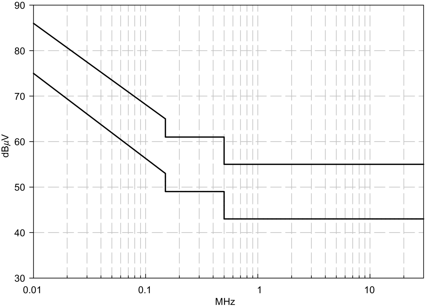
In the United States, it is the Federal Communications Commission (FCC) that sets the general EMC requirements, but medical products are regulated by the Food and Drug Administration (FDA). The FCC rules and regulations, title 47, part 15, subpart B concerns any unintentional radiator (device or system) that generates and uses timing pulses at a rate in excess of 9000 pulses (cycles) per second and uses digital techniques. Clearly, that mandatory requirement applies to almost every product that employs a microprocessor. It is illegal to sell or advertise for the sale of any product regulated under part 15, subpart B until its emissions have been measured and found to be in compliance. Products regulated by part 15, subpart B are divided in two classes. Class A devices are those marketed for use in commercial applications, whereas the domestic applications belong to class B. As illustrated in Fig. 42.23, class B limits are more stringent than those for class A products, and the class B administrative certification process is more rigorous than the class A verification process. The American National Standards Institute (ANSI) standard C63.4 defines the required emission test procedures. However, there are no FCC regulations pertaining to product immunity to electromagnetic fields.
EMC requirements for products used by the US military are listed in the already mentioned MIL-STD-461. This standard is applicable to a wide range of systems, from power tools to computer workstations. Unlike the FCC regulations, MIL-STD-461 specifies limits for both the emissions and immunity. The ANSI and Institute of Electrical and Electronics Engineers (IEEE) also publish EMC standards, as do, for internal use, private organizations, such as the Society of Automotive Engineers (SAE) and automobile manufacturers.
Under provisions of the General Agreement on Tariffs and Trade (GATT) and its successor, the World Trade Organization (WTO), member countries are obliged to adopt international standards for national use. With respect to the EMC, international standards are primarily developed by the International Electrotechnical Commission (IEC) and its International Special Committee on Radio Interference (CISPR); both were already mentioned in the introduction to this chapter. The series of IEC standards, IEC 61000-1 through IEC 61000-6, covers all aspects of EMC. The FCC standards are harmonized to IEC standards, as are the European Norms (EN) used in the European Union (EU). Some specific EMC standards have also been published by the International Organization for Standardization (ISO).
In 1992, the EU eliminated internal borders, necessitating a common system for establishing EMC standards and accreditation, testing, and certification procedures. The “new approach” and “global approach” have been initiated; their goal are to include EU directives into national laws of EU states, harmonize national standards with the European standards, and ensure validity of test reports and conformity certificates between all member states.
According to the “new approach,” technical contents have been removed from the European directives and entrusted to the European standard bodies, which are Comitè Europèen de Normalization (CEN), Comitè Europèen de Normalization Electrotechnique (CENELEC), and European Telecommunication Standards Institute (ETSI). The key European directive 89/336/EEC “electromagnetic compatibility” gives only a general definition of the essential protection requirements for all electric and electronic equipment and systems while referring to CENELEC and ETSI standards for technical details. The “global approach” requires every product on the European market to have the permanent “CE” marking, which indicates that the affixer declares and takes full responsibility of the conformity to all applicable European directives.
The EMC directive 89/336/EEC sets up emission and immunity requirements. It defines (a) components, (b) systems, and (c) installations. The directive applies only to components performing direct function and to the systems. Standards referred to the directive are divided into basic standards, generic standards, and product standards. The basic standards define general EMC requirements and testing procedures, without specifying any limit values or assessment criteria. Generic standards specify the requirements for products in specific electromagnetic environments. For instance, EN 50081-1 applies to emissions in residential, commercial, and light industrial equipment, including power supplies for industrial equipment, and EN 50081-2 to emissions in industrial environments. Respective immunity norms are EN 50082-1 and EN 50082-2. Product standards address EMC requirements for certain products and product families, such as household appliances, information technology equipment, or generic light industrial equipment; various European norms are employed as the product standards.
The IEC 555-2 (EN 60555-2), IEC 1000-3-2 (EN 61000-3-2), and IEC 1000-3-4 are emission standards for low-frequency harmonics, closely associated with operation of power electronic converters. Voltage fluctuations and flicker (impression of unsteadiness of visual sensation induced by a light stimulus whose luminance or spectral distribution fluctuates in time) emission limits are defined in IEC 555-3 (EN 555-3), IEC 1000-3-3 (EN 61000-3-3), and IEC 1000-3-5. IEC 61000-4-7 and IEC 61000-4-15 define the required instrumentation for EMI measurements. Radio-frequency conducted and radiated emissions are dealt with in EN 55011, EN 55014, and EN 55022, whereas CISPR 16 is the basic standard for radio-interference measurements. Finally, IEC 1000-4-1 through IEC 1000-4-12 are immunity standards.
EMC standards are continuously being developed and revised. Therefore, it is important to keep track of standards' publication dates (DoP) and dates of withdrawal (DoW) of conflicting earlier standards. Temporary EN standards are called ENV. Numerous Internet resources are available, in particular:
• American National Standards Institute (ANSI)
• Canadian Standards Association
• Electronic Industries Association (EIA)
• European Telecommunications Standards Institute (ETSI)
• Federal Communications Commission (FCC)
• IEEE Standards Association
• International Electrotechnical Commission (IEC)
• International Organization for Standardization (ISO)
• National Institute of Standards and Technology (NIST)
• NSSN, A National Resource for Global Standards
• Society of Automotive Engineers (SAE)
• Standards Australia
• VCCI (Japanese EMC Regulation and Certification)
• Verband Deutscher Elektrotechniker e. V. (VDE–German standards)
For more EMC information links, go to http://www.dbtechnology.co.uk/links.htm and
https://en.wikipedia.org/wiki/List_of_common_EMC_test_standards. A comprehensive treatment of contemporary EMC issues in power electronic and power distribution systems can be found in [13,14].