Example 35.9
Output voltage control in three-phase voltage-source inverters using sinusoidal wave PWM (SPWM) and space-vector modulation (SVM)
Sinusoidal wave PWM
Voltage-source three-phase inverters (Fig. 35.21) are often used to drive squirrel cage induction motors (IM) in variable speed applications.
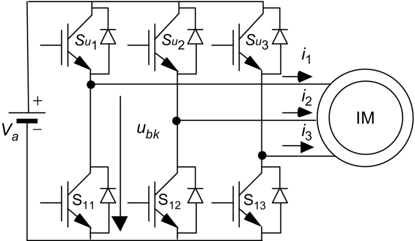
Considering almost ideal power semiconductors, the output voltage ubk(k∈{1, 2, 3}) dynamics of the inverter is negligible as the output voltage can hardly be considered a state variable in the time scale describing the motor behavior. Therefore, the best known method to create sinusoidal output voltages uses an open-loop modulator with low-frequency sinusoidal waveforms sin(ωt), with the amplitude defined by the modulation index mi (mi∈[0, 1]), modulating high-frequency triangular waveforms r(t) (carriers) (Fig. 35.22), a process similar to the one described in Section 35.2.4. The frequency and phase of the triangular carriers should guarantee half-wave and quarter-wave symmetry for minimum harmonic distortion.

This sinusoidal wave PWM (SPWM) modulator generates the variable γk, represented in Fig. 35.22 by the rectangular waveform, which describes the inverter k leg state:
γk={1→whenmisin(ωt)>r(t)0→whenmisin(ωt)<r(t)

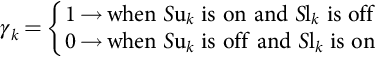
The turn-on and turn-off signals for the k leg inverter switches are related with the variable γk as follows:
γk={1→whenSukisonandSlkisoff0→whenSukisoffandSlkison
This applies constant-frequency sinusoidally weighted PWM signals to the gates of each insulated-gate bipolar transistor (IGBT). The PWM signals for all the upper IGBTs (Suk, k∈{1, 2, 3}) must be 120° out of phase, and the PWM signal for the lower IGBT Slk must be the complement of the Suk signal. Since transistor turn-on times are usually shorter than turn-off times, some dead time must be included between the Suk and Slk pulses to prevent internal short circuits.
Sinusoidal PWM can be easily implemented using a microprocessor or two digital counters/timers generating the addresses for two lookup tables (one for the triangular function and another for supplying the per unit basis of the sine, whose frequency can vary). Tables can be stored in read-only memories, ROM, or erasable programmable ROM, EPROM. One multiplier for the modulation index (perhaps into the digital-to-analog (D/A) converter for the sine ROM output) and one hysteresis comparator must also be included.
With SPWM, the first harmonic maximum amplitude of the obtained line-to-line voltage is only about 86% of the inverter dc supply voltage Va. Since it is expectable that this amplitude should be closer to Va, different modulating voltages (e.g., adding a third-order harmonic with one-fourth of the fundamental sine amplitude) can be used as long as the fundamental harmonic of the line-to-line voltage is kept sinusoidal. Another way is to leave SPWM and consider the eight possible inverter output voltages trying to directly use then. This will lead to space-vector modulation.
Space vector modulation
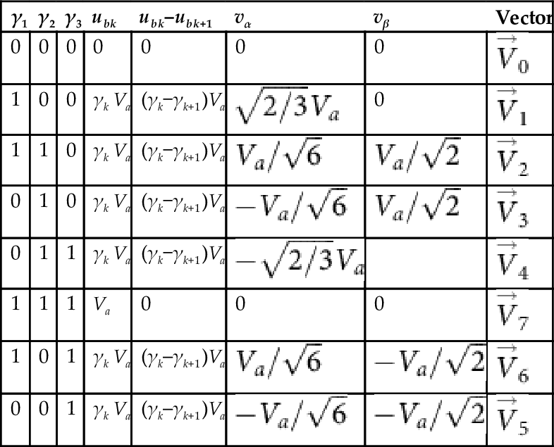
Space vector modulation (SVM) is based on the polar representation (Fig. 35.23) of the eight possible base output voltages of the three-phase inverter (Table 35.1, where vα and vβ are the vector components of vector →Vg,g∈{0,1,2,3,4,5,6,7}![]() , obtained with Eq. (35.72)). Therefore, as all the available voltages can be used, SVM does not present the voltage limitation of SPWM.
, obtained with Eq. (35.72)). Therefore, as all the available voltages can be used, SVM does not present the voltage limitation of SPWM.
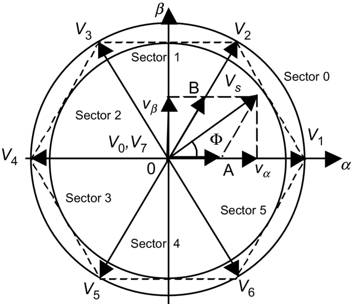
Table 35.1
The three-phase inverter with eight possible γk combinations, vector numbers, and respective α and β components
| γ1 | γ2 | γ3 | ubk | ubk−ubk+1 | vα | vβ | Vector |
| 0 | 0 | 0 | 0 | 0 | 0 | 0 | →V0 |
| 1 | 0 | 0 | γk Va | (γk−γk+1)Va | √2/3Va |
0 | →V1 |
| 1 | 1 | 0 | γk Va | (γk−γk+1)Va | Va/√6 |
Va/√2 |
→V2 |
| 0 | 1 | 0 | γk Va | (γk−γk+1)Va | −Va/√6 |
Va/√2 |
→V3 |
| 0 | 1 | 1 | γk Va | (γk−γk+1)Va | −√2/3Va |
→V4 | |
| 1 | 1 | 1 | Va | 0 | 0 | 0 | →V7 |
| 1 | 0 | 1 | γk Va | (γk–γk+1)Va | Va/√6 |
−Va/√2 |
→V6 |
| 0 | 0 | 1 | γk Va | (γk–γk+1)Va | −Va/√6 |
−Va/√2 |
→V5 |
Furthermore, being a vector technique, SVM fits nicely with the vector control methods often used in IM drives:
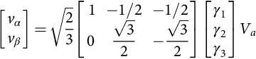
[vαvβ]=√23[1−1/2−1/20√32−√32][γ1γ2γ3]Va
Consider that the vector →Vs![]() (magnitude Vs and angle [Fcy]) must be applied to the IM. Since there is no such vector available directly, SVM uses an averaging technique to apply the two vectors, →V1
(magnitude Vs and angle [Fcy]) must be applied to the IM. Since there is no such vector available directly, SVM uses an averaging technique to apply the two vectors, →V1![]() and →V2
and →V2![]() , closest to →Vs
, closest to →Vs![]() . The vector →V1
. The vector →V1![]() will be applied during δATs, while vector →V2
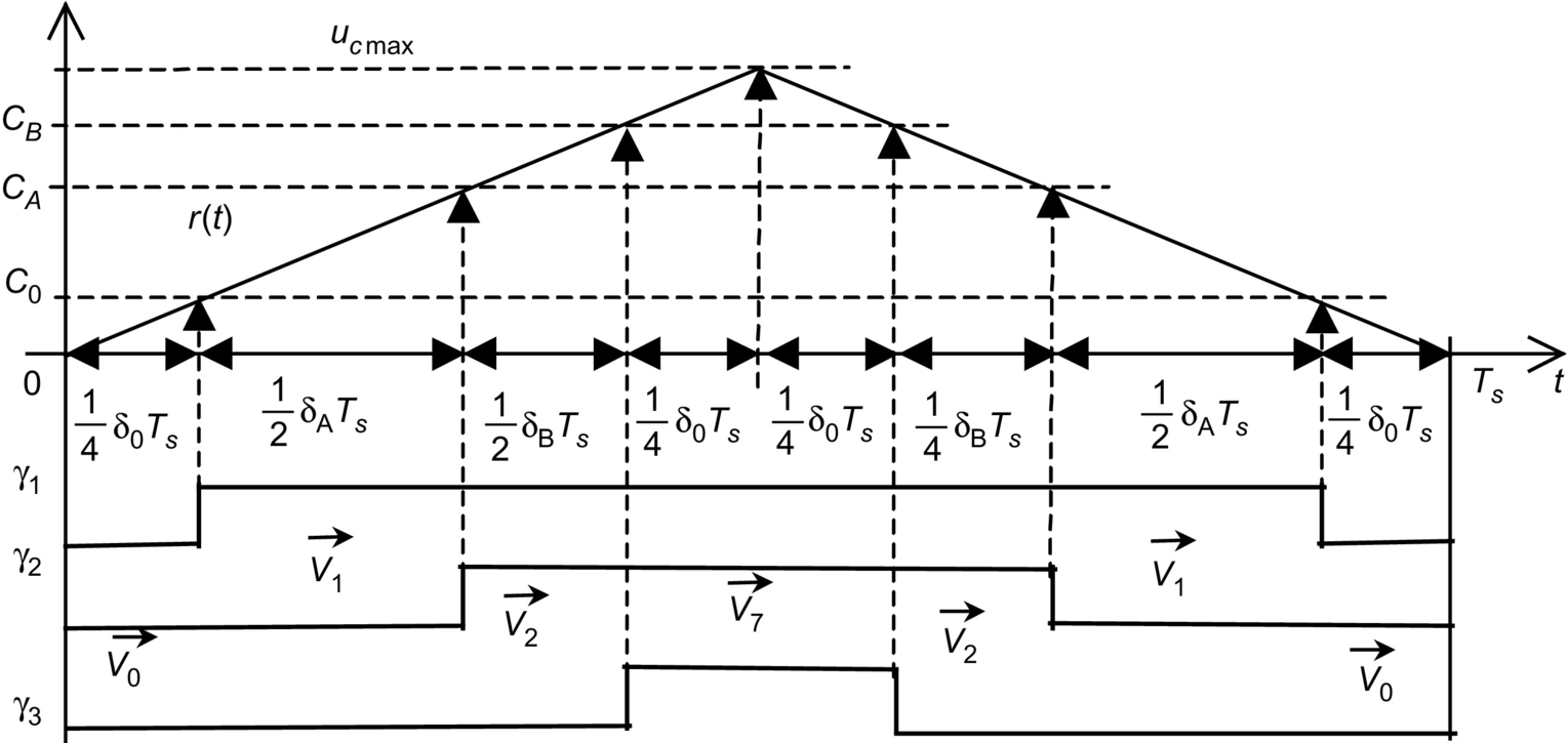
will be applied during δATs, while vector →V2![]() will last δBTs (where 1/Ts is the inverter switching frequency and δA and δB are duty cycles, δA and δB∈[0, 1]). If there is any leftover time in the PWM period Ts, then the zero vector is applied during time δ0Ts=Ts−δATs−δBTs. Since there are two zero vectors (→V0
will last δBTs (where 1/Ts is the inverter switching frequency and δA and δB are duty cycles, δA and δB∈[0, 1]). If there is any leftover time in the PWM period Ts, then the zero vector is applied during time δ0Ts=Ts−δATs−δBTs. Since there are two zero vectors (→V0![]() and →V7
and →V7![]() ), a symmetrical PWM can be devised, which uses both →V0
), a symmetrical PWM can be devised, which uses both →V0![]() and →V7
and →V7![]() , as shown in Fig. 35.24. Such a PWM arrangement minimizes the power semiconductor switching frequency and IM torque ripples
, as shown in Fig. 35.24. Such a PWM arrangement minimizes the power semiconductor switching frequency and IM torque ripples
The input to the SVM algorithm is the space vector →Vs![]() , into the sector sn, with magnitude Vs and angle Φs. This vector can be rotated to fit into sector 0 (Fig. 35.23) reducing Φs to the first sector, Φ=Φs−snπ/3. For any →Vs
, into the sector sn, with magnitude Vs and angle Φs. This vector can be rotated to fit into sector 0 (Fig. 35.23) reducing Φs to the first sector, Φ=Φs−snπ/3. For any →Vs![]() that is not exactly along one of the six nonnull inverter base vectors (Fig. 35.23), SVM must generate an approximation by applying the two adjacent vectors during an appropriate amount of time. The algorithm can be devised considering that the projections of →Vs
that is not exactly along one of the six nonnull inverter base vectors (Fig. 35.23), SVM must generate an approximation by applying the two adjacent vectors during an appropriate amount of time. The algorithm can be devised considering that the projections of →Vs![]() , onto the two closest base vectors, are values proportional to δA and δB duty cycles. Using simple trigonometric relations in sector 0 (0<Φ<π/3) (Fig. 35.23) and considering KT the proportional ratio, δA and δB are, respectively, δA=KT¯OA
, onto the two closest base vectors, are values proportional to δA and δB duty cycles. Using simple trigonometric relations in sector 0 (0<Φ<π/3) (Fig. 35.23) and considering KT the proportional ratio, δA and δB are, respectively, δA=KT¯OA![]() and δB=KT¯OA
and δB=KT¯OA![]() , yielding
, yielding
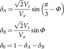
δA=KT2Vs√3sin(π3−Φ)δB=KT2Vs√3sinΦ

The KT value can be found if we notice that when →Vs=→V1![]() , δA=1, and δB=0 (or when →Vs=→V2
, δA=1, and δB=0 (or when →Vs=→V2![]() , δA=0, and δB=1). Therefore, since when →Vs=→V1
, δA=0, and δB=1). Therefore, since when →Vs=→V1![]() , Vs=√v2α+v2β=√2/3Va
, Vs=√v2α+v2β=√2/3Va![]() , Φ=0, or when →Vs=→V2
, Φ=0, or when →Vs=→V2![]() , Vs=√2/3Va
, Vs=√2/3Va![]() , Φ=π/3, the KT constant is KT=√3/(√2Va)
, Φ=π/3, the KT constant is KT=√3/(√2Va)![]() . Hence,
. Hence,
δA=√2VsVasin(π3−Φ)δB=√2VsVasinΦδ0=1−δA−δB
The obtained resulting vector →Vs![]() cannot extend beyond the hexagon of Fig. 35.23. This can be understood if the maximum magnitude Vsm of a vector with Φ=π/6 is calculated. For Φ=π/6, the maximum duty cycles are δA=1/2 and δB=1/2. Then, from Eq. (35.74,) Vsm=Va/√2
cannot extend beyond the hexagon of Fig. 35.23. This can be understood if the maximum magnitude Vsm of a vector with Φ=π/6 is calculated. For Φ=π/6, the maximum duty cycles are δA=1/2 and δB=1/2. Then, from Eq. (35.74,) Vsm=Va/√2![]() is obtained. This magnitude is lower than that of the vector →V1
is obtained. This magnitude is lower than that of the vector →V1![]() since the ratio between these magnitudes is √3/2
since the ratio between these magnitudes is √3/2![]() . To generate sinusoidal voltages, the vector →Vs
. To generate sinusoidal voltages, the vector →Vs![]() must be inside the inner circle of Fig. 35.23, so that it can be rotated without crossing the hexagon boundary. Vectors with tips between this circle and the hexagon are reachable but produce nonsinusoidal line-to-line voltages.
must be inside the inner circle of Fig. 35.23, so that it can be rotated without crossing the hexagon boundary. Vectors with tips between this circle and the hexagon are reachable but produce nonsinusoidal line-to-line voltages.
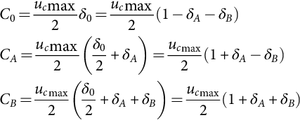
For sector 0 (Fig. 35.23), SVM symmetrical PWM switching variables (γ1, γ2, and γ3) and intervals (Fig. 35.24) can be obtained by comparing a triangular wave with amplitude ucmax (Fig. 35.24, where r(t)=2ucmaxt/Ts and t∈[0, Ts/2]), with the following values:
C0=ucmax2δ0=ucmax2(1−δA−δB)CA=ucmax2(δ02+δA)=ucmax2(1+δA−δB)CB=ucmax2(δ02+δA+δB)=ucmax2(1+δA+δB)
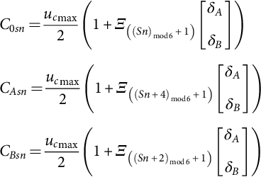
Extension of Eq. (35.75) to all six sectors can be done if the sector number sn is considered, together with the auxiliary matrix Ξ:
ΞT=[−1−1111−1−1111−1−1]

Generalization of the values C0, CA, and CB, denoted C0sn, CAsn, and CBsn, is written in Eq. (35.77), knowing that, for example, Ξ((sn+4)mod6+1)![]() is the Ξ matrix row with number (sn+4)mod 6+1:
is the Ξ matrix row with number (sn+4)mod 6+1:
C0sn=ucmax2(1+Ξ((Sn)mod6+1)[δAδB])CAsn=ucmax2(1+Ξ((Sn+4)mod6+1)[δAδB])CBsn=ucmax2(1+Ξ((Sn+2)mod6+1)[δAδB])
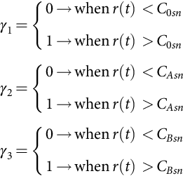
Therefore, γ1, γ2, and γ3 are
γ1={0→whenr(t)<C0sn1→whenr(t)>C0snγ2={0→whenr(t)<CAsn1→whenr(t)>CAsnγ3={0→whenr(t)<CBsn1→whenr(t)>CBsn
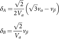
Supposing that the space vector →Vs![]() is now specified in the orthogonal coordinates α,β(→Vα,→Vβ)
is now specified in the orthogonal coordinates α,β(→Vα,→Vβ)![]() , instead of magnitude Vs and angle Φs, the duty cycles δA and δB can be easily calculated knowing that vα=Vs cos Φ and vβ=Vs sin Φ and using Eq. (35.74):
, instead of magnitude Vs and angle Φs, the duty cycles δA and δB can be easily calculated knowing that vα=Vs cos Φ and vβ=Vs sin Φ and using Eq. (35.74):
δA=√22Va(√3vα−vβ)δB=√2Vavβ
This equation enables the use of Eqs. (35.77) and (35.78) to obtain SVM in orthogonal coordinates.
Using SVM or SPWM, the closed-loop control of the inverter output currents (induction motor stator currents) can be performed using an approach similar to that outlined in Example 35.6 and decoupling the currents expressed in a d and q rotating frame.
35.3 Sliding-Mode Control of Switching Power Converters
35.3.1 Introduction
All the designed controllers for switching power converters are in fact variable structure controllers, in the sense that the control action changes rapidly from one to another of, usually, two possible δ(t) values, cyclically changing the converter topology. This is accomplished by the modulator (Fig. 35.6), which creates the switching variable δ(t) imposing δ(t)=1 or δ(t)=0, to turn on or off the power semiconductors. As a consequence of this discontinuous control action, indispensable for efficiency reasons, state trajectories move back and forth around a certain average surface in the state-space, and variables present some ripple. To avoid the effects of this ripple in the modeling and to apply linear control methodologies to time-variant systems, average values of state variables and state-space averaged models or circuits were presented (Section 35.2). However, a nonlinear approach to the modeling and control problem, taking advantage of the inherent ripple and variable structure behavior of switching power converters, instead of just trying to live with them, would be desirable, especially if enhanced performances could be attained.
In this approach, switching power converter topologies, as discrete nonlinear time-variant systems, are controlled to switch from one dynamics to another when just needed. If this switching occurs at a very high frequency (theoretically infinite), the state dynamics described as in Eq. (35.4) can be enforced to slide along a certain prescribed state-space trajectory. The converter is said to be in sliding mode, the allowed deviations from the trajectory (the ripple) imposing the practical switching frequency.
Sliding-mode control of variable structure systems, such as switching power converters, is particularly interesting because of the inherent robustness [10,11], capability of system order reduction, and appropriateness to the on/off switching of power semiconductors. The control action, being the control equivalent of the management paradigm “just in time” (JIT), provides timely and precise control actions, determined by the control law and the allowed ripple. Therefore, the switching frequency is not constant over all operating regions of the converter.
This section treats the derivation of the control (sliding surface) and switching laws, robustness, stability, constant-frequency operation, and steady-state error elimination necessary for sliding-mode control of switching power converters, also giving some examples.
35.3.2 Principles of Sliding-mode Control
Consider the state-space switched model Eq. (35.4) of a switching converter subsystem and input-output linearization or another technique, to obtain, from state-space equations, one Eq. (35.80), for each controllable subsystem output y=x. In the controllability canonical form [12] (also known as input-output decoupled or companion form), Eq. (35.80) is
ddt[xh,…xj−1,xj]T=[xh+1,…,xj,−fh(x)−ph(t)+bh(x)uh(t)]T
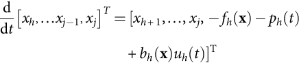
where x=[xh, …, xj−1, xj]T is the subsystem state vector, fh(x) and bh(x) are functions of x, ph(t) represents the external disturbances, and uh(t) is the control input. In this special form of state-space modeling, the state variables are chosen so that the xi+1 variable (i∈{h, …, j−1}) is the time derivative of xi, that is, x=[xh,˙xh,xh,…,mxh]T![]() , where m=j−h [13].
, where m=j−h [13].
35.3.2.1 Control Law (Sliding Surface)
The required closed-loop dynamics for the subsystem output vector y=x can be chosen to verify Eq. (35.81) with selected ki values. This is a model reference adaptive control approach to impose a state trajectory that advantageously reduces the system order (j−h+1):
dxjdt=−∑j−1i=hkikjxi+1
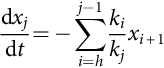
Effectively, in a single-input single-output (SISO) subsystem, the order is reduced by unity, applying the restriction Eq. (35.81). In a multiple-input multiple-output (MIMO) system, in which ν-independent restrictions could be imposed (usually with ν degrees of freedom), the order could often be reduced in ν units. Indeed, from Eq. (35.81), the dynamics of the jth term of x is linearly dependent from the j−h first terms:
dxjdt=−∑j−1i=hkikjxi+1=−∑j−1i=hkikjdxidt

The controllability canonical model allows the direct calculation of the needed control input to achieve the desired dynamics Eq. (35.81). In fact, as the control action should enforce the state vector x, to follow the reference vector xr=[xhr,˙xhr,¨xhr,…,mxhr]T![]() , the tracking error vector will be e=[xhr−xh,…,xj−1r−xj−1,xjr−xj]T
, the tracking error vector will be e=[xhr−xh,…,xj−1r−xj−1,xjr−xj]T![]() or e=[exh,…,exj−1,exj]T
or e=[exh,…,exj−1,exj]T![]() . Thus, equating the subexpressions for dxj/dt of Eqs. (35.80) and (35.81), the necessary control input uh(t) is
. Thus, equating the subexpressions for dxj/dt of Eqs. (35.80) and (35.81), the necessary control input uh(t) is
uh(t)=ph(t)+fh(x)+dxjdtbh(x)=ph(t)+fh(x)−j−1∑i=hkikjxi+1r+j−1∑i=hkikjexi+1bh(x)

This expression is the required closed-loop control law, but unfortunately, it depends on the system parameters and on external perturbations and is difficult to compute. Moreover, for some output requirements, Eq. (35.83) would give extremely high values for the control input uh(t), which would be impractical or almost impossible.
In most switching power converters, uh(t) is discontinuous. Yet, if we assume one or more discontinuity borders dividing the state-space into subspaces, the existence and uniqueness of the solution are guaranteed out of the discontinuity borders, since in each subspace the input is continuous. The discontinuity borders are subspace switching hypersurfaces, whose order is the space order minus one, along which the subsystem state slides, since its intersections with the auxiliary equations defining the discontinuity surfaces can give the needed control input.
Within the sliding-mode control (SMC) theory, assuming a certain dynamic error driven to zero, one auxiliary equation (sliding surface) and the equivalent control input uh(t) can be obtained, integrating both sides of Eq. (35.82) with null initial conditions:
kixj+∑j−1i=hkixi=∑ji=hkixi=0
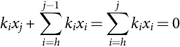
This equation represents the discontinuity surface (hyperplane) and just defines the necessary sliding surface S(xi, t) to obtain the prescribed dynamics of Eq. (35.81):
S(xi,t)=j∑i=hkixi=0
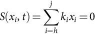
In fact, by taking the first time derivative of S(xi, t), ˙S(xi,t)=0![]() ; solving it for dxj/dt; and substituting the result in Eq. (35.83), the dynamics specified by Eq. (35.81) is obtained. This means that the control problem is reduced to a first-order problem, since it is only necessary to calculate the time derivative of Eq. (35.85) to obtain the dynamics (35.81) and the needed control input uh(t).
; solving it for dxj/dt; and substituting the result in Eq. (35.83), the dynamics specified by Eq. (35.81) is obtained. This means that the control problem is reduced to a first-order problem, since it is only necessary to calculate the time derivative of Eq. (35.85) to obtain the dynamics (35.81) and the needed control input uh(t).
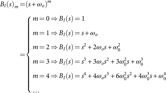
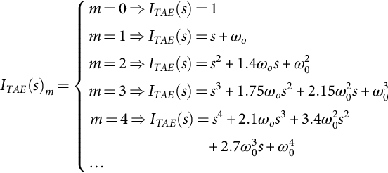
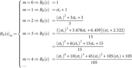
The sliding surface Eq. (35.85), as the dynamics of the converter subsystem, must be a Routh-Hurwitz polynomial and verify the sliding manifold invariance conditions, S(xi, t)=0 and ˙S(xi,t)=0![]() . Consequently, the closed-loop controlled system behaves as a stable system of order j−h, whose dynamics is imposed by the coefficients ki, which can be chosen by pole placement of the poles of the order m=j−h polynomial. Alternatively, certain kinds of polynomials can be advantageously used [14]: Butterworth, Bessel, Chebyshev, elliptic (or Cauer), binomial, and minimum integral of time absolute error product (ITAE). Most useful are Bessel polynomials BE(s) (Eq. (35.88)), which minimize the system response time tr, providing no overshoot; the polynomials ITAE(s) (Eq. (35.87)) that minimize the ITAE criterion for a system with desired natural oscillating frequency ωo; and binomial polynomials BI(s) (Eq. (35.86)). For m>1, ITAE polynomials give faster responses than binomial polynomials:
. Consequently, the closed-loop controlled system behaves as a stable system of order j−h, whose dynamics is imposed by the coefficients ki, which can be chosen by pole placement of the poles of the order m=j−h polynomial. Alternatively, certain kinds of polynomials can be advantageously used [14]: Butterworth, Bessel, Chebyshev, elliptic (or Cauer), binomial, and minimum integral of time absolute error product (ITAE). Most useful are Bessel polynomials BE(s) (Eq. (35.88)), which minimize the system response time tr, providing no overshoot; the polynomials ITAE(s) (Eq. (35.87)) that minimize the ITAE criterion for a system with desired natural oscillating frequency ωo; and binomial polynomials BI(s) (Eq. (35.86)). For m>1, ITAE polynomials give faster responses than binomial polynomials:
BI(s)m=(s+ωo)m={m=0⇒BI(s)=1m=1⇒BI(s)=s+ωom=2⇒BI(s)=s2+2ωos+ω20m=3⇒BI(s)=s3+3ωos2+3ω20s+ω30m=4⇒BI(s)=s4+4ωos3+6ω20s2+4ω30s+ω40…
ITAE(s)m={m=0⇒ITAE(s)=1m=1⇒ITAE(s)=s+ωom=2⇒ITAE(s)=s2+1.4ωos+ω20m=3⇒ITAE(s)=s3+1.75ωos2+2.15ω20s+ω30m=4⇒ITAE(s)=s4+2.1ωos3+3.4ω20s2+2.7ω30s+ω40…
BE(s)m={m=0⇒BE(s)=1m=1⇒BE(s)=str+1m=2⇒BE(s)=(str)2+3str+33m=3⇒BE(s)=((str)2+3.678str+6.459)(str+2.322)15=(stt)3+6(str)2+15str+1515m=4⇒BE(s)=(str)4+10(str)3+45(str)2+105(str)+105105…
These polynomials can be the reference model for this model reference adaptive control method.
35.3.2.2 Closed-Loop Control Input–Output Decoupled Form
For closed-loop control applications, instead of the state variables xi, it is worthy to consider, as new state variables, the errors exi![]() , components of the error vector e=[exh,˙exh,exh,…,mxxh]T
, components of the error vector e=[exh,˙exh,exh,…,mxxh]T![]() of the state-space variables xi, relative to a given reference xir
of the state-space variables xi, relative to a given reference xir![]() Eq. (35.90). The new controllability canonical model of the system is
Eq. (35.90). The new controllability canonical model of the system is
ddt[exh,…,exj−1,exj]T=[exh+1,…,exj,−fe(e)+pe(t)−be(e)uh(t)]T
where fe(e), pe(t), and be(e) are functions of the error vector e.
As the transformation of variables
exi=xir−xiwithi=h,…,j
is linear, the Routh-Hurwitz polynomial for the new sliding surface S(exi,t)![]() is
is
S(exi,t)=j∑i=hkiexi=0

Since exi+1(s)=sexi(s)![]() , this control law, from Eqs. (35.86) to (35.88), can be written as S(e,s)=exi(s+ωo)m
, this control law, from Eqs. (35.86) to (35.88), can be written as S(e,s)=exi(s+ωo)m![]() and is robust as it does not depend on circuit parameters, disturbances, or operating conditions, but only on the imposed ki parameters and on the state variable errors exi
and is robust as it does not depend on circuit parameters, disturbances, or operating conditions, but only on the imposed ki parameters and on the state variable errors exi![]() , which can usually be measured or estimated. The control law Eq. (35.91) enables the desired dynamics of the output variable(s), if the semiconductor switching strategy is designed to guarantee the system stability. In practice, the finite switching frequency of the semiconductors will impose a certain dynamic error ɛ steered to zero. The control law Eq. (35.91) is the required controller for the closed-loop SISO subsystem with output y.
, which can usually be measured or estimated. The control law Eq. (35.91) enables the desired dynamics of the output variable(s), if the semiconductor switching strategy is designed to guarantee the system stability. In practice, the finite switching frequency of the semiconductors will impose a certain dynamic error ɛ steered to zero. The control law Eq. (35.91) is the required controller for the closed-loop SISO subsystem with output y.
35.3.2.3 Stability
Existence condition. The existence of the operation in sliding mode implies S(exi,t)=0![]() . Also, to stay in this regime, the control system should guarantee ˙S(exi,t)=0
. Also, to stay in this regime, the control system should guarantee ˙S(exi,t)=0![]() . Therefore, the semiconductor switching law must ensure the stability condition for the system in sliding mode, written as
. Therefore, the semiconductor switching law must ensure the stability condition for the system in sliding mode, written as
S(exi,t)˙S(exi,t)<0
The fulfillment of this inequality ensures the convergence of the system state trajectories to the sliding surface S(exi,t)=0![]() , since
, since
– if S(exi,t)>0![]() and ˙S(exi,t)<0
and ˙S(exi,t)<0![]() , then S(exi,t)
, then S(exi,t)![]() will decrease to zero,
will decrease to zero,
– if S(exi,t)<0![]() and ˙S(exi,t)>0
and ˙S(exi,t)>0![]() , then S(exi,t)
, then S(exi,t)![]() will increase toward zero.
will increase toward zero.
Hence, if Eq. (35.92) is verified, then S(exi,t)![]() will converge to zero. The condition (35.92) is the manifold S(exi,t)
will converge to zero. The condition (35.92) is the manifold S(exi,t)![]() invariance condition or the sliding-mode existence condition.
invariance condition or the sliding-mode existence condition.
Given the state-space model Eq. (35.89) as a function of the error vector e and, from ˙S(exi,t)=0![]() , the equivalent average control input Ueq(t) that must be applied to the system in order that the system state slides along the surface, Eq. (35.91) is given by
, the equivalent average control input Ueq(t) that must be applied to the system in order that the system state slides along the surface, Eq. (35.91) is given by
Ueq(t)=khdexhdt+kh+1dexh+1dt+…+kj−1+dexj−1dt+kj(−fe(e)+pe(t))kjbe(e)
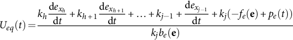
This control input Ueq(t) ensures the converter subsystem operation in the sliding mode.
Reaching condition. The fulfillment of S(exi,t)˙S(exi,t)<0![]() as S(exi,t)˙S(exi,t)=(1/2)˙S2(exi,t)
as S(exi,t)˙S(exi,t)=(1/2)˙S2(exi,t)![]() implies that the distance between the system state and the sliding surface will tend to zero, since S2(exi,t)
implies that the distance between the system state and the sliding surface will tend to zero, since S2(exi,t)![]() can be considered as a measure for this distance. This means that the system will reach sliding mode. Additionally, from Eq. (35.89), it can be written as
can be considered as a measure for this distance. This means that the system will reach sliding mode. Additionally, from Eq. (35.89), it can be written as
dexjdt=−fe(e)+pe(t)−be(e)uh(t)
From Eq. (35.91), Eq. (35.95) is obtained:
S(exi,t)=∑ji=hkiexi=khexh+kh+1dexhdt+kh+2d2exhdt2+…+kjdmexhdtm
If S(exi,t)>0![]() , from the Routh-Hurwitz property of Eq. (35.91), then exj>0
, from the Routh-Hurwitz property of Eq. (35.91), then exj>0![]() . In this case, to reach S(exi,t)=0
. In this case, to reach S(exi,t)=0![]() , it is necessary to impose−be(e)uh(t)=−U in Eq. (35.94), with U chosen to guarantee dexj/dt<0
, it is necessary to impose−be(e)uh(t)=−U in Eq. (35.94), with U chosen to guarantee dexj/dt<0![]() . After a certain time, exj
. After a certain time, exj![]() will be exj=dmexh/dtm<0
will be exj=dmexh/dtm<0![]() , implying along with Eq. (35.95) that ˙S(exi,t)<0
, implying along with Eq. (35.95) that ˙S(exi,t)<0![]() , thus verifying Eq. (35.92). Therefore, every term of S(exi,t)
, thus verifying Eq. (35.92). Therefore, every term of S(exi,t)![]() will be negative, which implies, after a certain time, an error exh<0
will be negative, which implies, after a certain time, an error exh<0![]() and S(exi,t)<0
and S(exi,t)<0![]() . Hence, the system will reach sliding mode, staying there if U=Ueq(t). This same reasoning can be made for S(exi,t)<0
. Hence, the system will reach sliding mode, staying there if U=Ueq(t). This same reasoning can be made for S(exi,t)<0![]() ; it is now being necessary to impose−be(e)uh(t)=+U, with U high enough to guarantee dexj/dt>0
; it is now being necessary to impose−be(e)uh(t)=+U, with U high enough to guarantee dexj/dt>0![]() .
.
To ensure that the system always reaches sliding-mode operation, it is necessary to calculate the maximum value of Ueq(t) and Ueqmax and also impose the reaching condition:
U>Ueqmax
This means that the power supply voltage values U should be chosen high enough to additionally account for the maximum effects of the perturbations. With step inputs, even with U>Ueqmax, the converter usually loses sliding mode, but it will reach it again, even if the Ueqmax is calculated considering only the maximum steady-state values for the perturbations.
35.3.2.4 Switching Law
From the foregoing considerations, supposing a system with two possible structures, the semiconductor switching strategy must ensure S(exi,t)˙S(exi,t)<0![]() . Therefore, if S(exi,t)>0
. Therefore, if S(exi,t)>0![]() , then ˙S(exi,t)<0
, then ˙S(exi,t)<0![]() , which implies, as seen, −be(e)uh(t)=−U (the sign of be(e) must be known). Also, if S(exi,t)<0
, which implies, as seen, −be(e)uh(t)=−U (the sign of be(e) must be known). Also, if S(exi,t)<0![]() , then ˙S(exi,t)>0
, then ˙S(exi,t)>0![]() , which implies−be(e)uh(t)=+U. This imposes the switching between two structures at infinite frequency. Since power semiconductors can only switch at finite frequency, in practice, a small enough error for S(exi,t)
, which implies−be(e)uh(t)=+U. This imposes the switching between two structures at infinite frequency. Since power semiconductors can only switch at finite frequency, in practice, a small enough error for S(exi,t)![]() must be allowed (−ɛ<S(exi,t)<+ɛ)
must be allowed (−ɛ<S(exi,t)<+ɛ)![]() . Hence, the switching law between the two possible system structures might be
. Hence, the switching law between the two possible system structures might be
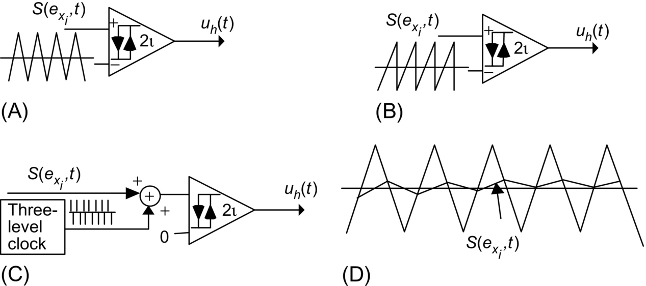
uh(t)={U/be(e)forS(exi,t)>+ε−U/be(e)forS(exi,t)<−ε
The condition Eq. (35.97) determines the control input to be applied and therefore represents the semiconductor switching strategy or switching function. This law determines a two-level pulse-width modulator with JIT switching (variable frequency).
35.3.2.5 Robustness
The dynamics of a system, with closed-loop control using the control law Eq. (35.91) and the switching law Eq. (35.97), does not depend on the system operating point, load, circuit parameters, power supply, or bounded disturbances, as long as the control input uh(t) is large enough to maintain the converter subsystem in sliding mode. Therefore, it is said that the switching power converter dynamics, operating in sliding mode, is robust against changing operating conditions, variations of circuit parameters, and external disturbances. The desired dynamics for the output variable(s) is determined only by the ki coefficients of the control law Eq. (35.91), as long as the switching law (35.97) maintains the converter in sliding mode.
35.3.3 Constant-Frequency Operation
Prefixed switching frequency can be achieved, even with the sliding-mode controllers, at the cost of losing the JIT action. As the sliding-mode controller changes the control input when needed and not at a certain prefixed rhythm, applications needing constant switching frequency (such as thyristor rectifiers or resonant converters) must compare S(exi, t) (hysteresis width 2ι much narrower than 2ɛ) with auxiliary triangular waveforms (Fig. 35.25A), auxiliary sawtooth functions (Fig. 35.25B), three-level clocks (Fig. 35.25C), or phase-locked loop control of the comparator hysteresis variable width 2ɛ [15]. However, as illustrated in Fig. 35.25D, steady-state errors do appear. Often, they should be eliminated as described in Section 35.3.4.
35.3.4 Steady-State Error Elimination in Converters with Continuous Control Inputs
In the ideal sliding mode, state trajectories are directed toward the sliding surface (35.91) and move exactly along the discontinuity surface, switching between the possible system structures at infinite frequency. Practical sliding modes cannot switch at infinite frequency and therefore exhibit phase-plane trajectory oscillations inside a hysteresis band of width 2ɛ, centered in the discontinuity surface.
The switching law Eq. (35.91) permits no steady-state errors as long as S(exi,t)![]() tends to zero, which implies no restrictions on the commutation frequency. Control circuits operating at constant frequency or needed continuous inputs or particular limitations of the power semiconductors, such as minimum on or off times, can originate S(exi,t)=ɛ1≠0
tends to zero, which implies no restrictions on the commutation frequency. Control circuits operating at constant frequency or needed continuous inputs or particular limitations of the power semiconductors, such as minimum on or off times, can originate S(exi,t)=ɛ1≠0![]() . The steady-state error (exh)
. The steady-state error (exh)![]() of the xh variable xhr−xh=ɛ1/kh
of the xh variable xhr−xh=ɛ1/kh![]() can be eliminated, increasing the system order by 1. The new state-space controllability canonical form, considering the error exj
can be eliminated, increasing the system order by 1. The new state-space controllability canonical form, considering the error exj![]() , between the variables and their references, as the state vector, is
, between the variables and their references, as the state vector, is
ddt[∫,exh,d,t,,,exh,,,…,,,exj−1,,,exj]T=[exh,exh+1,…,exj,−fe(e)−pe(t)−be(e)uh(t)]T
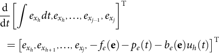
The new sliding surface S(exi,t)![]() written from Eq. (35.91), considering the new system in Eq. (35.98), is
written from Eq. (35.91), considering the new system in Eq. (35.98), is
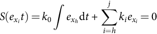
S(exi,t)=k0∫exhdt+∑ji=hkiexi=0
This sliding surface offers zero-state error, even if S(exi,t)=ɛ1![]() due to the hardware errors or fixed (or limited) frequency switching. Indeed, at the steady state, the only nonzero term is k0∫exhdt=ɛ1
due to the hardware errors or fixed (or limited) frequency switching. Indeed, at the steady state, the only nonzero term is k0∫exhdt=ɛ1![]() . Also, like Eq. (35.91), this closed-loop control law does not depend on system parameters or perturbations to ensure a prescribed closed-loop dynamics similar to Eq. (35.81) with an error approaching zero.
. Also, like Eq. (35.91), this closed-loop control law does not depend on system parameters or perturbations to ensure a prescribed closed-loop dynamics similar to Eq. (35.81) with an error approaching zero.
The approach outlined herein precisely defines the control law (sliding surface (35.91) or (35.99)) needed to obtain the selected dynamics and the switching law Eq. (35.97). As the control law allows the implementation of the system controller and the switching law gives the PWM modulator, there is no need to design linear or nonlinear controllers, based on linear converter models, or devise offline PWM modulators. Therefore, sliding-mode control theory, applied to switching power converters, provides a systematic method to generate both the controller(s) (usually nonlinear) and the modulator(s) that will ensure a model reference robust dynamics, solving the control problem of switching power converters.
In the next examples, it is shown that the sliding-mode controllers use (nonlinear) state feedback, therefore, needing to measure the state variables and often other variables, since they use more system information. This is a disadvantage since more sensors are needed. However, the straightforward control design and obtained performances are much better than those obtained with the averaged models, the use of more sensors being really valued. Alternatively to the extra sensors, state observers can be used [12,13].
35.3.5 Examples: Buck–Boost DC/DC Converter, Half-bridge Inverter, 12-Pulse Parallel Rectifiers, Audio Power Amplifiers, Near Unity Power Factor Rectifiers, Multilevel Inverters, Matrix Converters
Example 35.10
Sliding-mode control of the buck–boost dc/dc converter
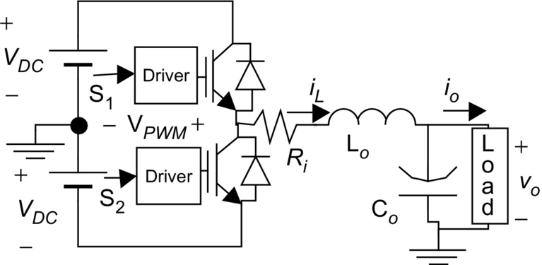
Consider again the buck-boost converter of Fig. 35.1 and assume the converter output voltage vo to be the controlled output. From Section 35.2, using the switched state-space model of Eq. (35.11), making dvo/dt=θ, and calculating the first time derivative of θ, the controllability canonical model (35.100), where io=vo/Ro, is obtained:
dvodt=θ=1−δ(t)CoiL−ioCodθdt=−(1−δ(t))2LiCovo−Coθ+ioCo(1−δ(t))dδ(t)dt−1Codiodt+δ(t)(1−δ(t))CoLiVDC
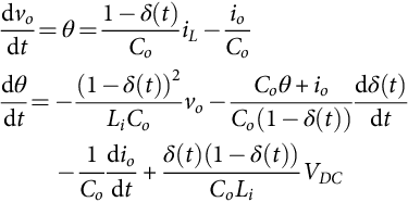
This model, written in the form of Eq. (35.80), contains two state variables, vo and θ. Therefore, from Eq. (35.91) and considering evo=vor−vo,eθ=θr−θ![]() , the control law (sliding surface) is
, the control law (sliding surface) is
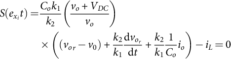
S(exi,t)=∑2i=hkiexi=k1(vor−vo)+k2dvordt−k2dvodt=k1(vor−vo)+k2dvordt−k2Co(1−δ(t))iL+k2Coio=0
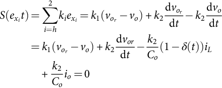
This sliding surface depends on the variable δ(t), which should be precisely the result of the application, in Eq. (35.101), of a switching law similar to Eq. (35.97). Assuming an ideal up-down converter and slow variations, from Eq. (35.31), the variable δ(t) can be averaged to δ1=vo/(vo+VDC). Substituting this relation in Eq. (35.101) and rearranging, Eq. (35.102) is derived:
S(exi,t)=Cok1k2(vo+VDCvo)×((vor−v0)+k2k1dvordt+k2k11Coio)−iL=0
This control law shows that the power supply voltage VDC must be measured, as well as the output voltage vo and the currents io and iL.
To obtain the switching law from stability considerations (35.92), the time derivative of S(exi,t)![]() , supposing (vo+VDC)/vo almost constant, is
, supposing (vo+VDC)/vo almost constant, is
˙S(exi,t)=Cok1k2(vo+VDCvo)×(devodt+k2k1d2vordt2+k2k1Codiodt)−diLdt

If S(exi,t)>0![]() , then, from Eq. (35.92), ˙S(exi,t)<0
, then, from Eq. (35.92), ˙S(exi,t)<0![]() must hold. Analyzing Eq. (35.103), we can conclude that, if S(exi,t)>0
must hold. Analyzing Eq. (35.103), we can conclude that, if S(exi,t)>0![]() , ˙S(exi,t)
, ˙S(exi,t)![]() is negative if, and only if, diL/dt>0. Therefore, for positive errors evo>0
is negative if, and only if, diL/dt>0. Therefore, for positive errors evo>0![]() , the current iL must be increased, which implies δ(t)=1. Similarly, for S(exi,t)<0
, the current iL must be increased, which implies δ(t)=1. Similarly, for S(exi,t)<0![]() , diL/dt<0, and δ(t)=0. Thus, a switching law similar to Eq. (35.97) is obtained:
, diL/dt<0, and δ(t)=0. Thus, a switching law similar to Eq. (35.97) is obtained:
δ(t)={1forS(exi,t)>+e0forS(exi,t)<−e
The same switching law could be obtained from knowing the dynamic behavior of this nonminimum-phase up-down converter: to increase (decrease) the output voltage, a previous increase (decrease) of the iL current is mandatory.
Eq. (35.101) shows that, if the buck-boost converter is into the sliding mode (S(exi,t)=0)![]() , the dynamics of the output voltage error tends exponentially to zero with time constant k2/k1 (k2/k1>0). Since during step transients, the converter is in the reaching mode, the time constant k2/k1 cannot be designed to originate error variations larger than the one allowed by the self-dynamics of the converter excited by a certain maximum permissible iL current. Given the polynomials (35.86–35.88) with m=1, k1/k2=ωo should be much lower than the finite switching frequency (1/T) of the converter. Therefore, the time constant must obey k2/k1≫T. Then, knowing that k2 and k1 are both imposed, the control designer can tailor the time constant as needed, provided that the above restrictions are observed.
, the dynamics of the output voltage error tends exponentially to zero with time constant k2/k1 (k2/k1>0). Since during step transients, the converter is in the reaching mode, the time constant k2/k1 cannot be designed to originate error variations larger than the one allowed by the self-dynamics of the converter excited by a certain maximum permissible iL current. Given the polynomials (35.86–35.88) with m=1, k1/k2=ωo should be much lower than the finite switching frequency (1/T) of the converter. Therefore, the time constant must obey k2/k1≫T. Then, knowing that k2 and k1 are both imposed, the control designer can tailor the time constant as needed, provided that the above restrictions are observed.
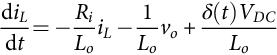
Short-circuit-proof operation for the sliding-mode-controlled buck-boost converter can be derived from Eq. (35.102), noting that all the terms to the left of iL represent the set point for this current. Therefore, limiting these terms (Fig. 35.26, saturation block, with iLmax=40 A), the switching law (35.104) ensures that the output current will not rise above the maximum imposed limit. Given the converter nonminimum-phase behavior, this iL current limit is fundamental to reach the sliding mode of operation with step disturbances.
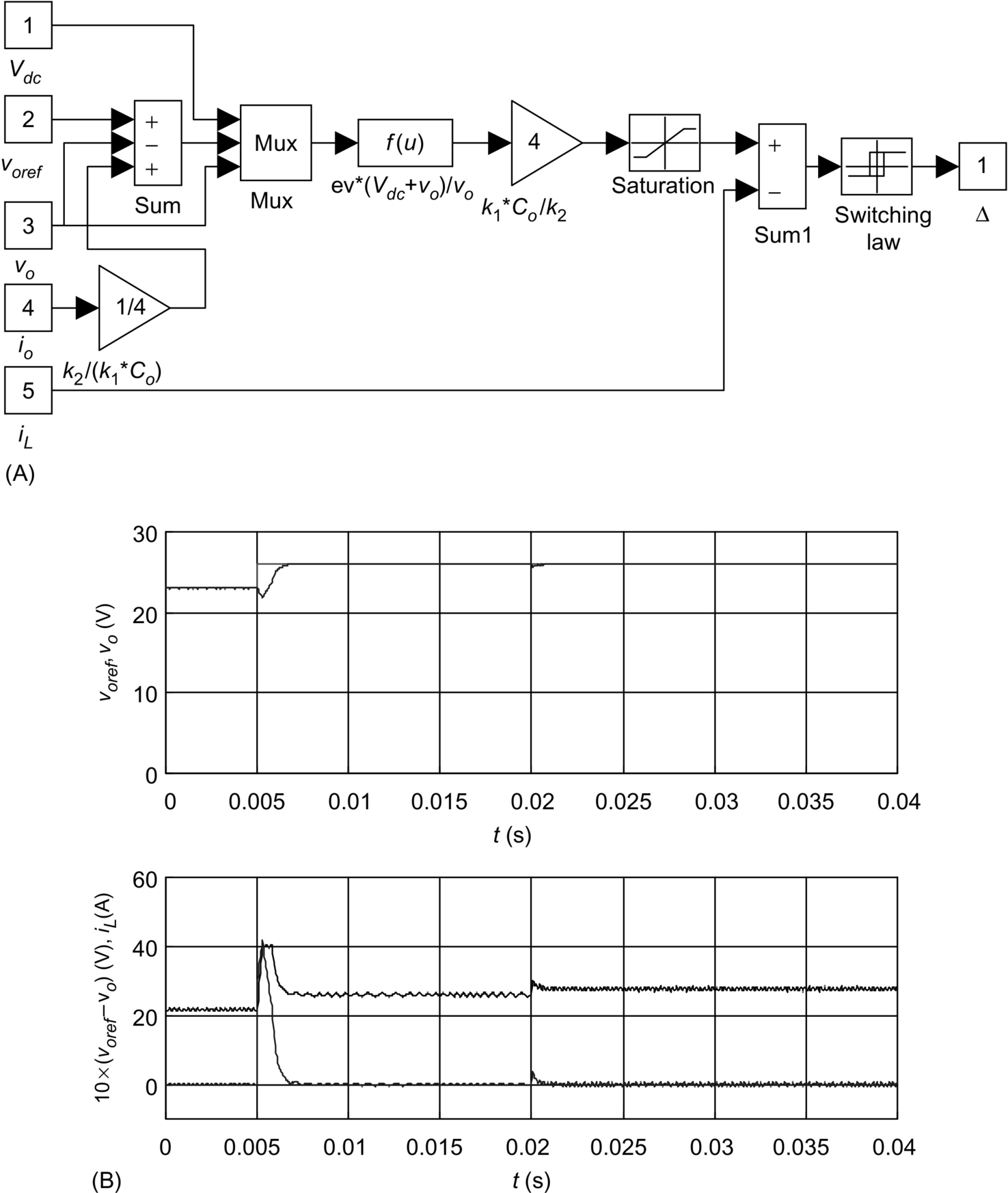
The block diagram (Fig. 35.26A) of the implemented control law Eq. (35.102) (with Cok1/k2=4) and switching law (35.103) (with ɛ=0.3) does not include the time derivative of the reference (dvor/dt)![]() since, in a dc/dc converter, its value is considered zero. The controller hardware (or software), derived using just the sliding-mode approach, operates only in a closed-loop.
since, in a dc/dc converter, its value is considered zero. The controller hardware (or software), derived using just the sliding-mode approach, operates only in a closed-loop.
The resulting performance (Fig. 35.26B) is much better than that obtained with the PID notch filter (compare with Example 35.4 and Fig. 35.9B), with a higher response speed and robustness against power supply variations.
35.3.5.1 Example 35.11: Sliding Mode Control of the Single-Phase Half-Bridge Converter
Consider the half-bridge four-quadrant converter of Fig. 35.27 with the output filter and the inductive load (VDCmax=300 V, VDCmin=230 V, Ri=0.1 Ω, Lo=4 mH, Co=470 μF, inductive load with nominal values Ro=7 Ω, and Lo=1 mH).
Assuming that power switches, output filter capacitor, and power supply are all ideal and a generic load with allowed slow variations, the switched state-space model of the converter, with state variables vo and iL, is
ddt[voiL]=[01/Co−1/Lo−Ri/Lo][voiL]+[−1/Co001/Lo][ioδ(t)VDC]

where io is the generic load current and vPWM=δ(t)VDC is the extended PWM output voltage (δ(t)=+1 when one of the upper main semiconductors of Fig. 35.27 is conducting and δ(t)=−1 when one of the lower semiconductors is on).
Output current control (current-mode control)
To perform as a viL![]() voltage-controlled iL current source (or sink) with transconductance gm (gm=iL/viL)
voltage-controlled iL current source (or sink) with transconductance gm (gm=iL/viL)![]() , this converter must supply a current iL to the output inductor, obeying iL=gmviL
, this converter must supply a current iL to the output inductor, obeying iL=gmviL![]() . Using a bounded viL
. Using a bounded viL![]() voltage to provide output short-circuit protection, the reference current for a sliding-mode controller must be iLr=gmviL
voltage to provide output short-circuit protection, the reference current for a sliding-mode controller must be iLr=gmviL![]() . Therefore, the controlled output is the iL current, and the controllability canonical model (35.106) is obtained from the second equation of (35.105), since the dynamics of this subsystem, being governed by δ(t)VDC, is already in the controllability canonical form for this chosen output:
. Therefore, the controlled output is the iL current, and the controllability canonical model (35.106) is obtained from the second equation of (35.105), since the dynamics of this subsystem, being governed by δ(t)VDC, is already in the controllability canonical form for this chosen output:
diLdt=−RiLoiL−1Lovo+δ(t)VDCLo
A suitable sliding surface (35.107) is obtained from Eq. (35.91), making eiL=iLr−iL![]() :
:
S(eiL,t)=kpeiL=kp(iLr−iL)=kp(gmviL−iL)=0
The switching law Eq. (35.108) can be devised calculating the time derivative of Eq. (35.107) ˙S(eiL,t)![]() and applying Eq. (35.92). If S(eiL,t)>0
and applying Eq. (35.92). If S(eiL,t)>0![]() , then diL/dt>0 must hold to obtain S(eiL,t)<0
, then diL/dt>0 must hold to obtain S(eiL,t)<0![]() , implying δ(t)=1:
, implying δ(t)=1:
δ(t)={1forS(eiL,t)>+ε−1forS(eiL,t)<−ε
The kp value and the allowed ripple ɛ define the instantaneous value of the variable switching frequency. The sliding-mode controller is represented in Fig. 35.28A. Step response (Fig. 35.29A) shows the variable-frequency operation, a very short rise time (limited only by the available power supply), and confirms the expected robustness against supply variations.

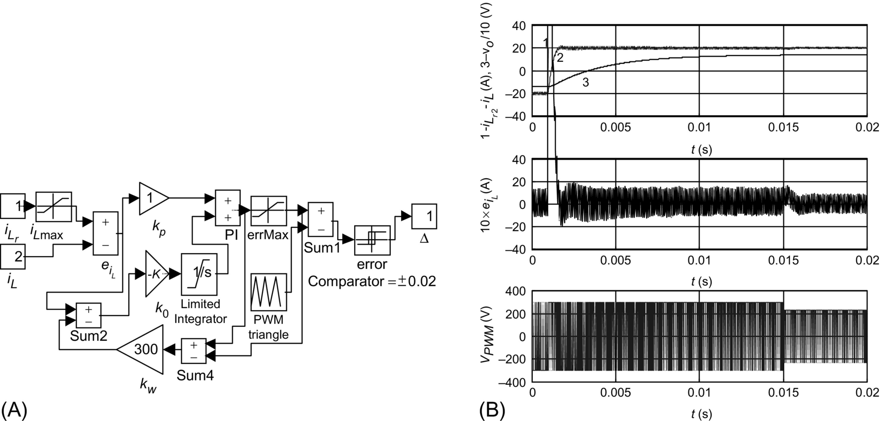
For systems where fixed-frequency operation is needed, a triangular wave, with frequency (10 kHz) slightly greater than the maximum variable frequency, can be added (Fig. 35.28B) to the sliding-mode controller, as explained in Section 35.3.3. Performances (Fig. 35.29B) are comparable with those of the variable-frequency sliding-mode controller (Fig. 35.29A). Fig. 35.29B shows not only the constant switching frequency but also a steady-state error dependent on the operating point.
To eliminate this error, a new sliding surface Eq. (35.109), based on Eq. (35.99), should be used. The constants kp and k0 can be calculated, as discussed in Example 35.10:
S(eiL,t)=k0∫eiLdt+kpeiL=0
The new constant-frequency sliding-mode current controller (Fig. 35.30A), with added antiwindup techniques (Example 35.6), since a saturation (errMax) is needed to keep the frequency constant, now presents no steady-state error (Fig. 35.30B). Performances are comparable with those of the variable-frequency controller, and no robustness loss is visible. The applied sliding-mode approach led to the derivation of the known average current-mode controller.
 step from −20 to 20 A at t=0.001 s and to a VDC step from 300 to 230 V at t=0.015 s.
Output voltage control
To obtain a power operational amplifier suitable for building uninterruptible power supplies, power filters, power gyrators, inductance simulators, or power factor active compensators, vo must be the controlled converter output. Therefore, using the input-output linearization technique, it is seen that the first time derivative of the output (dvo/dt)=(iL−io)/Co=θ does not explicitly contain the control input δ(t)VDC. Then, the second derivative must be calculated. Taking into account Eq. (35.105), as θ=(iL−io)/Co, Eq. (35.110) is derived
d2vodt2=ddtθ=ddt(iL−ioCo)=−RiLoθ−1LoCovo−RiLoCoio−1Codiodt+1LoCoδ(t)VDC
This expression shows that the second derivative of the output depends on the control input δ(t)VDC. No further time derivative is needed, and the state-space equations of the equivalent circuit, written in the phase canonical form, are
ddt[voθ]=[θ−RiLoθ−1LoCovo−RiLoCoio−1Codiodt+1LoCoδ(t)VDC]
According to Eqs. (35.91), (35.111), and (35.105), considering that evo![]() is the feedback error evo=vor−vo
is the feedback error evo=vor−vo![]() , a sliding surface S(evo,t)
, a sliding surface S(evo,t)![]() can be chosen:
can be chosen:
S(evo,t)=k1evo+k2devodt=evo+k2k1devodt=evo+βdevodt=Coβ(vor−vo)+Codvordt+io−iL=0

where β is the time constant of the desired first-order response of output voltage (β≫T>0), as the strong relative degree [13] of this system is 2, and the sliding-mode operation reduces by one, the order of this system (the strong relative degree of a system is the least positive integer r for which the rth derivative of the output drvo/dtr is an explicit function of the control input u, being divo/du=0 for 0≤i≤r−1 and drvo/du≠0).
Calculating ˙S(evo,t)![]() , the control strategy (switching law) Eq. (35.113) can be devised since, if S(evo,t)>0
, the control strategy (switching law) Eq. (35.113) can be devised since, if S(evo,t)>0![]() , then diL/dt must be positive to obtain ˙S(eiL,t)<0
, then diL/dt must be positive to obtain ˙S(eiL,t)<0![]() , implying δ(t)=1. Otherwise, δ(t)=−1:
, implying δ(t)=1. Otherwise, δ(t)=−1:
δ(t)={1forS(evo,t)>0(vPWM=+VDC)−1forS(evo,t)<0(vPWM=−VDC)

In the ideal sliding-mode dynamics, the filter input voltage vPWM switches between VDC and −VDC with the infinite frequency. This switching generates the equivalent control voltage Veq that must satisfy the sliding manifold invariance conditions, S(evo,t)=0![]() and ˙S(evo,t)=0
and ˙S(evo,t)=0![]() . Therefore, from ˙S(evo,t)=0
. Therefore, from ˙S(evo,t)=0![]() , using Eqs. (35.112) and (35.105) (or from Eq. (35.110)), Veq is
, using Eqs. (35.112) and (35.105) (or from Eq. (35.110)), Veq is
Veq=LoCo[d2vordt2+1βdvordt+voLoCo+(βRi−Lo)iLβLoCoioβCo+1Codiodt]

This equation shows that only smooth input vor![]() signals (“smooth” functions) can be accurately reproduced at the inverter output, as it contains derivatives of the vor
signals (“smooth” functions) can be accurately reproduced at the inverter output, as it contains derivatives of the vor![]() signal. This fact is a consequence of the stored electromagnetic energy. The existence of the sliding-mode operation implies the following necessary and sufficient condition:
signal. This fact is a consequence of the stored electromagnetic energy. The existence of the sliding-mode operation implies the following necessary and sufficient condition:
–VDC<Veq<VDC
Eq. (35.115) enables the determination of the minimum input voltage VDC needed to enforce the sliding-mode operation. Moreover, even in the case of |Veq|>|VDC|, the system experiences only a saturation transient and eventually reaches the region of sliding-mode operation, except if the operating point and disturbances enforce |Veq|>|VDC| in steady state.
In the ideal sliding mode, at infinite switching frequency, state trajectories are directed toward the sliding surface and move exactly along the discontinuity surface. Practical switching power converters cannot switch at infinite frequency, so a typical implementation of Eq. (35.112) (Fig. 35.31A) with neglected ˙vor![]() features a comparator with hysteresis 2ɛ, switching occurring at |S(evo,t)|>ɛ
features a comparator with hysteresis 2ɛ, switching occurring at |S(evo,t)|>ɛ![]() with frequency depending on the slopes of iL. This hysteresis causes phase-plane trajectory oscillations of width 2ɛ around the discontinuity surface S(evo,t)=0
with frequency depending on the slopes of iL. This hysteresis causes phase-plane trajectory oscillations of width 2ɛ around the discontinuity surface S(evo,t)=0![]() , but the Veq voltage is still correctly generated, since the resulting duty cycle is a continuous variable (except for error limitations in the hardware or software, which can be corrected using the approach pointed out by Eq. (35.98)).
, but the Veq voltage is still correctly generated, since the resulting duty cycle is a continuous variable (except for error limitations in the hardware or software, which can be corrected using the approach pointed out by Eq. (35.98)).
The design of the compensator and the modulator is integrated with the same theoretical approach, since the signal S(evo,t)![]() applied to a comparator generates the pulses for the power semiconductors drives. If the short-circuit-proof operation is built into the power semiconductor drives, there is the possibility to measure only the capacitor current (iL−io).
applied to a comparator generates the pulses for the power semiconductors drives. If the short-circuit-proof operation is built into the power semiconductor drives, there is the possibility to measure only the capacitor current (iL−io).
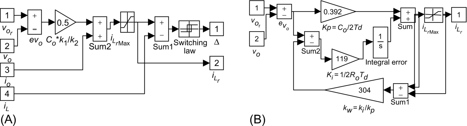
Short-circuit protection and fixed-frequency operation of the power operational amplifier
If we note that all the terms to the left of iL in Eq. (35.112) represent the value of iLr![]() , a simple way to provide short-circuit protection is to bound the sum of all these terms (Fig. 35.31A with iLrmax=100A
, a simple way to provide short-circuit protection is to bound the sum of all these terms (Fig. 35.31A with iLrmax=100A![]() ). Alternatively, the output current controllers of Fig. 35.28 can be used, comparing Eq. (35.107) with Eq. (35.112), to obtain iLr=S(evo,t)/kp+iL
). Alternatively, the output current controllers of Fig. 35.28 can be used, comparing Eq. (35.107) with Eq. (35.112), to obtain iLr=S(evo,t)/kp+iL![]() . Therefore, the block diagram of Fig. 35.31A provides the iLr
. Therefore, the block diagram of Fig. 35.31A provides the iLr![]() output (for kp=1) to be the input of the current controllers (Figs. 35.28 and 35.31A). As seen, the controllers of Figs. 35.28B and 35.30A also ensure fixed-frequency operation.
output (for kp=1) to be the input of the current controllers (Figs. 35.28 and 35.31A). As seen, the controllers of Figs. 35.28B and 35.30A also ensure fixed-frequency operation.
For comparison purposes, a proportional-integral (PI) controller, with antiwindup (Fig. 35.31B) for output voltage control, was designed, supposing the current-mode control of the half bridge (iLr=gmviL/(1+sTd)![]() considering a small delay Td) and a pure resistive load Ro and using the approach outlined in Examples 35.6 and 35.8 (kv=1, gm=1, ζ2=0.5, and Td=600 μs). The obtained PI (35.50) parameters are
considering a small delay Td) and a pure resistive load Ro and using the approach outlined in Examples 35.6 and 35.8 (kv=1, gm=1, ζ2=0.5, and Td=600 μs). The obtained PI (35.50) parameters are
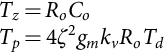
Tz=RoCoTp=4ζ2gmkvRoTd
Both variable frequency (Fig. 35.32) and constant frequency (Fig. 35.33) sliding-mode output voltage controllers present excellent performance and robustness with nominal loads. With loads much higher than the nominal value (Figs. 35.32B and 35.33B), the performance and robustness are also excellent. The sliding-mode constant-frequency PWM controller presents the additional advantage of injecting lower ripple in the load.
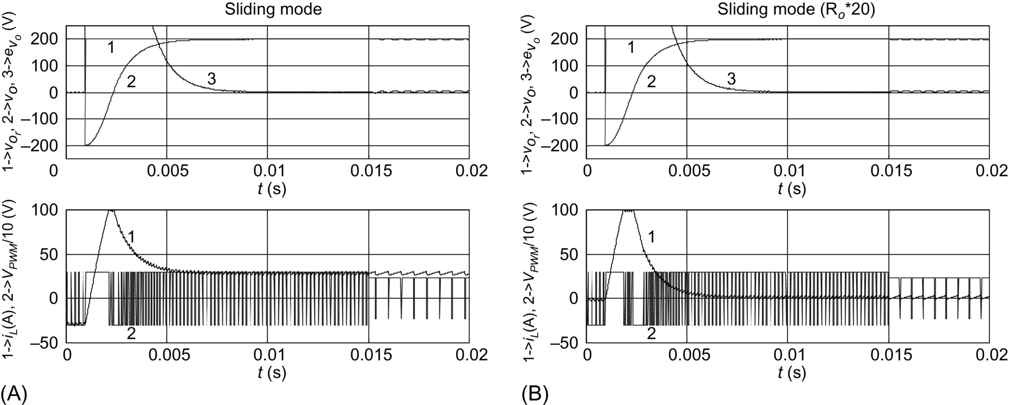
 step from −200 to 200 V at t=0.001 s and to a VDC step from 300 to 230 V at t=0.015 s: (A) variable-frequency sliding mode (nominal load) and (B) variable-frequency sliding mode (Ro×20).
 step from −200 to 200 V at t=0.001 s and to a VDC step from 300 to 230 V at t=0.015 s: (A) fixed-frequency sliding mode (nominal load) and (B) fixed-frequency sliding mode (Ro×20).
As expected, the PI regulator presents lower performance (Fig. 35.34). The response speed is lower, and the insensitivity to power supply and load variations (Fig. 35.34B) is not as high as with the sliding mode. Nevertheless, the PI performances are acceptable, since its design was carried considering a slow and fast manifold sliding-mode approach: the fixed-frequency sliding-mode current controller (35.109) for the fast manifold (the iL current dynamics) and the antiwindup PI for the slow manifold (the vo voltage dynamics, usually much slower than the current dynamics).
 step from −200 to 200 V at t=0.001 s and to a VDC step from 300 to 230 V at t=0.015 s: (A) PI current-mode controller (nominal load) and (B) PI current-mode controller (Ro×20).
35.3.5.2 Example 35.12: Constant-Frequency Sliding-Mode Control of p Pulse Parallel Rectifiers
This example presents a new paradigm to the control of thyristor rectifiers. Since p pulse rectifiers are variable-structure systems, sliding-mode control is applied here to 12-pulse rectifiers, still useful for very high-power applications [3]. The design determines the variables to be measured, and the controlled rectifier presents robustness and much shorter response times, even with the parameter uncertainty, perturbations, noise, and nonmodeled dynamics. These performances are not feasible using linear controllers, obtained here for comparison purposes.
Modeling the 12-pulse parallel rectifier
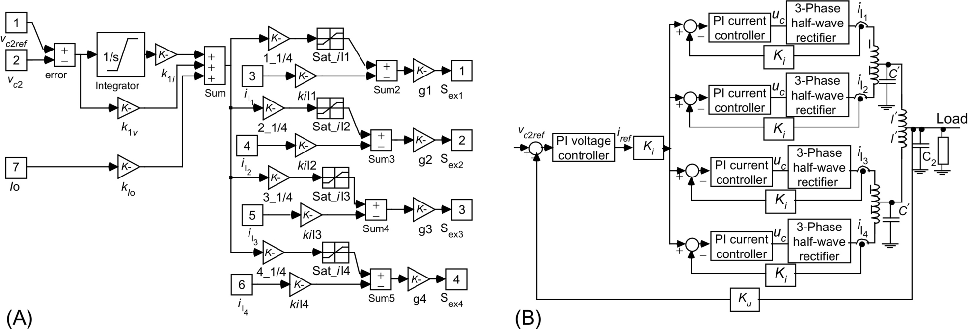
The 12-pulse rectifier (Fig. 35.35A) is built with four three-phase half-wave rectifiers, connected in parallel with current-sharing inductances l and l′ merged with capacitors C′ and C2, to obtain a second-order LC filter. This allows low-ripple output voltage and continuous mode of operation (laboratory model with l=44 mH, l′=13 mH, C′=C2=10 mF, star-delta-connected ac sources with ERMS≈65 V, and power rating 2.2 kW, load approximately resistive Ro≈3–5 Ω).
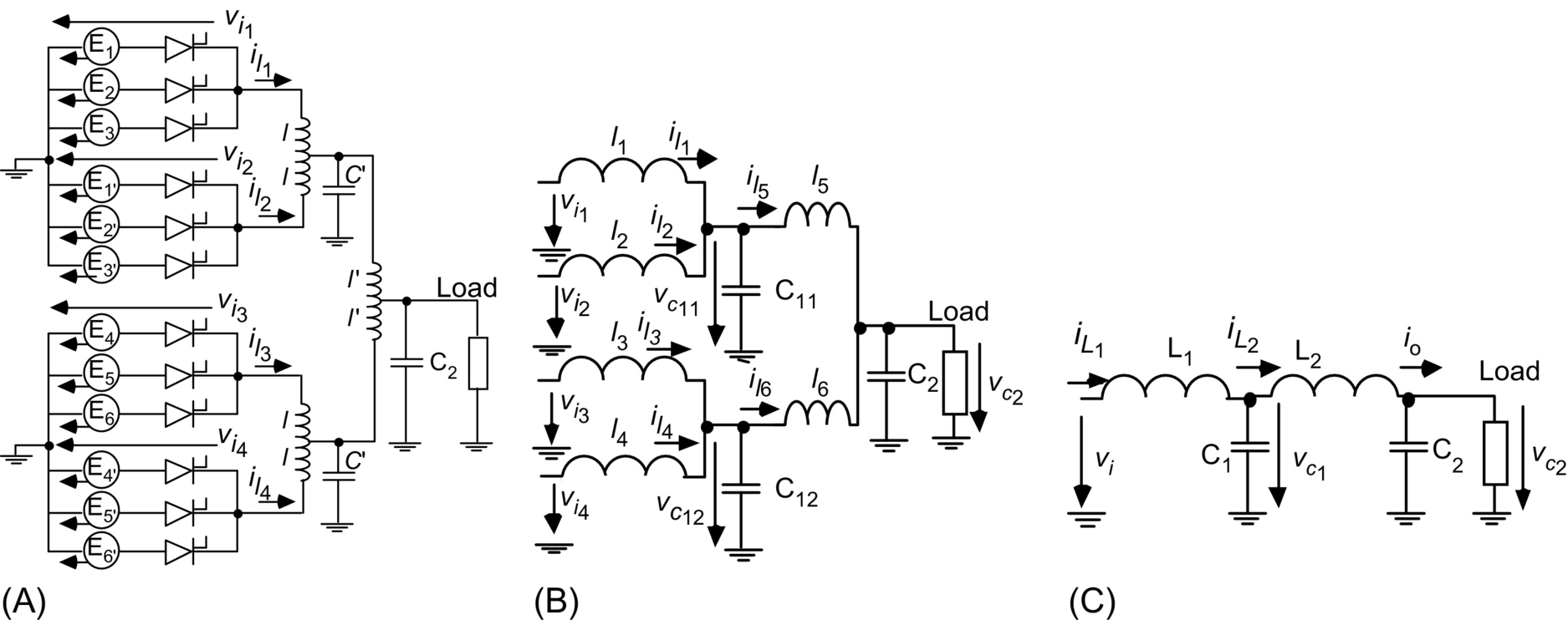
To control the output voltage vc2, given the complexity of the whole system, the best approach is to derive a low-order model. By averaging the four half-wave rectifiers, neglecting the rectifier dynamics and mutual couplings, the equivalent circuit of Fig. 35.35B is obtained (l1=l2=l3=l4=l, l5=l6=l′, and C11=C12=C′). Since the rectifiers are identical, the equivalent 12-pulse rectifier model of Fig. 35.35C is derived, simplifying the resulting parallel associations (L1=l/4, L2=l/2, and C1=2C′).
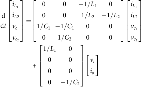
Considering the load current io as an external perturbation and vi the control input, the state-space model of the equivalent circuit of Fig. 35.35C is
ddt[iL1iL2vc1vc2]=[00−1/L10001/L2−1/L21/C1−1/C10001/C200][iL1iL2vc1vc2]+[1/L1000000−1/C2][viio]
Sliding-mode control of the 12-pulse parallel rectifier
Since the output voltage vc2![]() of the system must follow the reference vc2r
of the system must follow the reference vc2r![]() , the system equations in the phase canonical (or controllability) form must be written, using the error ev2=vc2r−vc2
, the system equations in the phase canonical (or controllability) form must be written, using the error ev2=vc2r−vc2![]() and its time derivatives as new state error variables, as done in Example 35.11:
and its time derivatives as new state error variables, as done in Example 35.11:
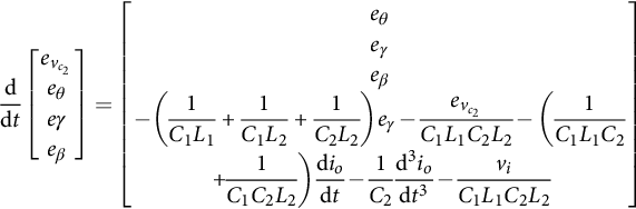
ddt[evc2eθeγeβ]=[eθeγeβ−(1C1L1+1C1L2+1C2L2)eγ−evc2C1L1C2L2−(1C1L1C2+1C1C2L2)diodt−1C2d3iodt3−viC1L1C2L2]
The sliding surface S(exi,t)![]() , designed to reduce the system order, is a linear combination of all the phase canonical state variables. Considering Eqs. (35.118) and (35.117) and the errors evc2
, designed to reduce the system order, is a linear combination of all the phase canonical state variables. Considering Eqs. (35.118) and (35.117) and the errors evc2![]() , eθ, eγ, and eβ, the sliding surface can be expressed as a combination of the rectifier currents, voltages, and their time derivatives:
, eθ, eγ, and eβ, the sliding surface can be expressed as a combination of the rectifier currents, voltages, and their time derivatives:
S(exi,t)=evc2+kθeθ+kγeγ+kβeβ=vc2r+kθθr+kγγr+kββr−(1−kγC2L2)vc2−kγC2L2vc1+(kθC2−kβC22L2)io+kγC2diodt+kβC2d2iodt2−kβC1C2L2iL1−(kθC2−kβC1C2L2−kβC22L2)iL2=0
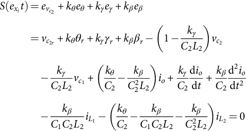
Eq. (35.119) shows the variables to be measured (vc2,vc1,io,iL1,andiL2)![]() . Therefore, it can be concluded that the output current of each three-phase half-wave rectifier must be measured.
. Therefore, it can be concluded that the output current of each three-phase half-wave rectifier must be measured.
The existence of the sliding mode implies S(exi,t)=0![]() and ˙S(exi,t)=0
and ˙S(exi,t)=0![]() . Given the state models (35.117) and (35.118) and from ˙S(exi,t)=0
. Given the state models (35.117) and (35.118) and from ˙S(exi,t)=0![]() , the available voltage of the power supply vi must exceed the equivalent average dc input voltage Veq (35.120), which should be applied at the filter input, in order that the system state slides along the sliding surface (35.119):
, the available voltage of the power supply vi must exceed the equivalent average dc input voltage Veq (35.120), which should be applied at the filter input, in order that the system state slides along the sliding surface (35.119):
Veq=C1L1C2L2kβ(θr+kθγr+kγβr+kβ˙βr)+vc2−C1L1C2L2kβ×(θ+kγβ)+(C2L2+C2L1+C1L1−C1L1C2L2kθkβ)γ+(L1+L2)diodt+C1L1L2d3iodt3

This means that the power supply root mean square (RMS) voltage values should be chosen high enough to account for the maximum effects of the perturbations. This is almost the same criterion adopted when calculating the RMS voltage values needed with linear controllers. However, as the Veq voltage contains the derivatives of the reference voltage, the system will not be able to stay in sliding mode with a step as the reference.
The switching law would be derived, considering that, from Eq. (35.97), be(e)>0. Therefore, from Eq. (35.119), if S(exi,t)>+ɛ![]() , then vi(t)=Veqmax
, then vi(t)=Veqmax![]() , else if S(exi,t)<−ɛ
, else if S(exi,t)<−ɛ![]() , then vi(t)=−Veqmax
, then vi(t)=−Veqmax![]() . However, because of the lack of gate turn-off capability of the rectifier thyristors, power rectifiers cannot generate the high-frequency switching voltage vi(t), since the statistical mean delay time is T/2p (T=20 ms) and reaches T/2 when switching from +Veqmax
. However, because of the lack of gate turn-off capability of the rectifier thyristors, power rectifiers cannot generate the high-frequency switching voltage vi(t), since the statistical mean delay time is T/2p (T=20 ms) and reaches T/2 when switching from +Veqmax![]() to −Veqmax
to −Veqmax![]() . To control mains switched rectifiers, the described constant-frequency sliding-mode operation method is used, in which the sliding surface S(exi,t)
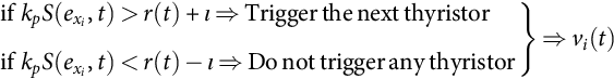
. To control mains switched rectifiers, the described constant-frequency sliding-mode operation method is used, in which the sliding surface S(exi,t)![]() instead of being compared with zero is compared with an auxiliary constant-frequency function r(t) (Fig. 35.6B) synchronized with the mains frequency. The new switching law is
instead of being compared with zero is compared with an auxiliary constant-frequency function r(t) (Fig. 35.6B) synchronized with the mains frequency. The new switching law is
ifkpS(exi,t)>r(t)+ι⇒TriggerthenextthyristorifkpS(exi,t)<r(t)−ι⇒Donottriggeranythyristor}⇒vi(t)
Since now S(exi,t)![]() is not near zero, but around some value of r(t), a steady-state error evc2av
is not near zero, but around some value of r(t), a steady-state error evc2av![]() appears (min[r(t)]/kp<evc2av<max[r(t)]/kp)
appears (min[r(t)]/kp<evc2av<max[r(t)]/kp)![]() , as seen in Example 35.11. Increasing the value of kp (toward the ideal saturation control) does not overcome this drawback, since oscillations would appear even for moderate kp gains, because of the rectifier dynamics. Instead, the sliding surface (35.122), based on Eq. (35.99), should be used. It contains an integral term, which, given the canonical controllability form and the Routh-Hurwitz property, is the only nonzero term at steady state, enabling the complete elimination of the steady-state error:
, as seen in Example 35.11. Increasing the value of kp (toward the ideal saturation control) does not overcome this drawback, since oscillations would appear even for moderate kp gains, because of the rectifier dynamics. Instead, the sliding surface (35.122), based on Eq. (35.99), should be used. It contains an integral term, which, given the canonical controllability form and the Routh-Hurwitz property, is the only nonzero term at steady state, enabling the complete elimination of the steady-state error:
Si(exi,t)=∫evc2dt+k1vevc2+k1θeθ+k1γeγ+k1βeβ

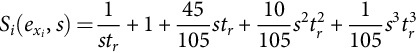
To determine the k constants of Eq. (35.122), a pole-placement technique is selected, according to a fourth-order Bessel polynomial BE(s)m, m=4, from Eq. (35.88), in order to obtain the smallest possible response time with almost no overshoot. For a delay characteristic as flat as possible, the delay tr is taken inversely proportional to a frequency fci just below the lowest cutoff frequency (fci<8.44 Hz) of the double LC filter. For this fourth-order filter, the delay is tr=2.8/(2πfci). By choosing fci=7 Hz (tr≈64 ms) and dividing all the Bessel polynomial terms by str, the characteristic polynomial (35.123) is obtained:
Si(exi,s)=1str+1+45105str+10105s2t2r+1105s3t3r
This polynomial must be applied to Eq. (35.122) to obtain the four sliding functions needed to derive the thyristor trigger pulses of the four three-phase half-wave rectifiers. These sliding functions will enable the control of the output current (il1,il2,il3andil4)![]() of each half-wave rectifier, improving the current sharing among them (Fig. 35.35B). Supposing equal current share, the relation between the iL1
of each half-wave rectifier, improving the current sharing among them (Fig. 35.35B). Supposing equal current share, the relation between the iL1![]() current and the output currents of each three-phase rectifier is iL1=4il1=4il2=4il3=4il4
current and the output currents of each three-phase rectifier is iL1=4il1=4il2=4il3=4il4![]() . Therefore, for the nth half-wave three-phase rectifier, since, for n=1 and n=2, vc1=vc11
. Therefore, for the nth half-wave three-phase rectifier, since, for n=1 and n=2, vc1=vc11![]() and iL2=2il5
and iL2=2il5![]() and, for n=3 and n=4, vc1=vc12
and, for n=3 and n=4, vc1=vc12![]() and iL2=2il6
and iL2=2il6![]() , the four sliding surfaces are (k1v=1)
, the four sliding surfaces are (k1v=1)
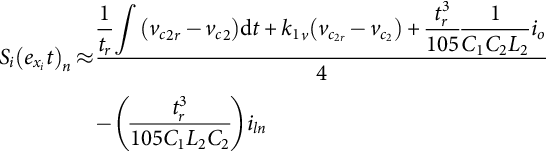
Si(exi,t)n=[k1vvc2r+45tr105θr+10t2r105γr+t3r105βr+1tr∫(vc2r−vc2)dt−(k1vC2L2−10t2r105C2L2)vc2−10t2r105C2L2vc1,2+(45tr105C2−t3r105C22L2)io+(10t2r105C2)diodt+(t3r105C2)d2iodt2]/4−[(45tr105C2−t3r105C22L2−t3r105C1L2C2)il5,6]/2−(t3r105C1L2C2)iln

If an inexpensive analog controller is desired, the successive time derivatives of the reference voltage and the output current of Eq. (35.124) can be neglected (furthermore, their calculation is noise prone). Nonzero errors on the first-, second-, and third-order derivatives of the controlled variable will appear, worsening the response speed. However, the steady-state error is not affected.
To implement the four equations (35.124), the variables vc2,vc11,vc12,io,il5,il6,il1,il2,il3andil4![]() must be measured. Although this could be done easily, it is very convenient to further simplify the practical controller, keeping its complexity and cost at the level of linear controllers, while maintaining the advantages of sliding mode. Therefore, the voltages vc11andvc12
must be measured. Although this could be done easily, it is very convenient to further simplify the practical controller, keeping its complexity and cost at the level of linear controllers, while maintaining the advantages of sliding mode. Therefore, the voltages vc11andvc12![]() are assumed almost constant over one period of the filter input current, and vc11=vc12=vc2
are assumed almost constant over one period of the filter input current, and vc11=vc12=vc2![]() , meaning that il5=il6=io/2
, meaning that il5=il6=io/2![]() . With these assumptions, valid as the values of C′ and C2 are designed to provide an output voltage with very low ripple, the new sliding-mode functions are
. With these assumptions, valid as the values of C′ and C2 are designed to provide an output voltage with very low ripple, the new sliding-mode functions are
Si(exi,t)n≈1tr∫(vc2r−vc2)dt+k1v(vc2r−vc2)+t3r1051C1C2L2io4−(t3r105C1L2C2)iln
These approximations disregard only the high-frequency content of vc11,vc12,il5,andil6![]() and do not affect the rectifier steady-state response, but the step response will be a little slower, although still much faster (150 ms, Fig. 35.39) than that obtained with linear controllers (280 ms, Fig. 35.38). Regardless of all the approximations, the low switching frequency of the rectifier would not allow the elimination of the dynamic errors. As a benefit of these approximations, the sliding-mode controller (Fig. 35.36A) will need only an extra current sensor (or a current observer) and an extra operational amplifier in comparison with linear controllers derived hereafter (which need four current sensors and six operational amplifiers). Compared with the total cost of the 12-pulse rectifier plus output filter, the control hardware cost is negligible in both cases, even for medium-power applications.
and do not affect the rectifier steady-state response, but the step response will be a little slower, although still much faster (150 ms, Fig. 35.39) than that obtained with linear controllers (280 ms, Fig. 35.38). Regardless of all the approximations, the low switching frequency of the rectifier would not allow the elimination of the dynamic errors. As a benefit of these approximations, the sliding-mode controller (Fig. 35.36A) will need only an extra current sensor (or a current observer) and an extra operational amplifier in comparison with linear controllers derived hereafter (which need four current sensors and six operational amplifiers). Compared with the total cost of the 12-pulse rectifier plus output filter, the control hardware cost is negligible in both cases, even for medium-power applications.