
18.4.4 Solid-State Marx Generators
The use of voltage multiplication techniques for generating HV repetitive pulses is not limited to the use of transformers. More complex methods can be used without the limitation of transformers. The most common is the Marx generator concept [55].
The Marx generator concept is presented in the circuit of Fig. 18.44, which comprises a number of modular stages constituted by an energy storage capacitor Ci, two impedances Zi (resistive and/or inductive) for charging and limiting the self-short-circuit capacitor paths and a switch Si, for i∈{1, 2, …,n}. During the charging period, a relatively low-voltage dc power supply Vdc charges the Ci capacitors in parallel through impedances Zi.

When switches Si are turned on, the Ci capacitors are connected in series and apply a voltage into the load, equal to
depending that the capacitors are charged to the power supply full voltage, Vdc. During this time, the bottom impedances Zi limit the self-short-circuit path of the Ci capacitors.
The circuit in Fig. 18.44 is assembled in such a way that there is voltage modularity, meaning that each stage holds the power supply voltage Vdc. However, due to this parallel process, the first stages carry the total charging current, which sets different power requirements for the devices in each stage.
This concept has been used intensively through the years, with spark gaps used as switch Si for very high-voltages and powers, but the spark gap only turns off when the current goes to zero. Recent technological upgrades with the addition of solid-state switches and the replacement of most of the passive elements increased the lifetime of the modulator and allowed higher pulse repetition rates, meaning an improved performance [22,56–58].
18.4.4.1 Generation of Negative Pulses
During the last years, various semiconductor-based Marx and SM topologies have been described, with analogous characteristics in order to reduce the losses and increase the performance of the circuit for different types of applications and loads [22,56–58].
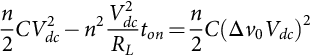
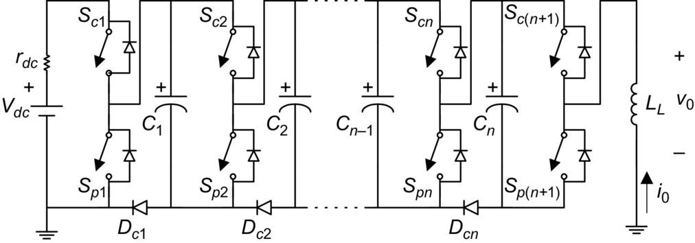
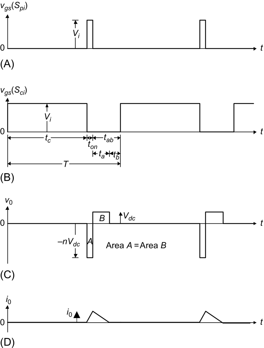
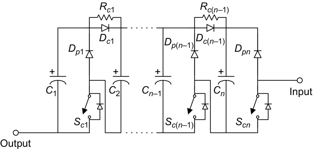
Fig. 18.45 shows a typical SM topology, with n stages able to deliver negative high-voltage repetitive pulses into a load RL; the theoretical key waveforms are shown in Fig. 18.46. Each stage of the SM consists of an energy storing capacitor Ci, a diode Dci, and two switches Sci and Spi, with antiparallel diodes, where the subscript i∈{1, 2, …, n−1, n, n+1}. The Si switches can be implemented with BJTs, GTOs, IGCTs, IGBTs, MOSFETS, or other on-off devices. The inclusion of Sc1 guarantees that during the pulse period, the dc charging power supply Vdc is not short-circuited, preventing high-current-load pulses through the power supply.
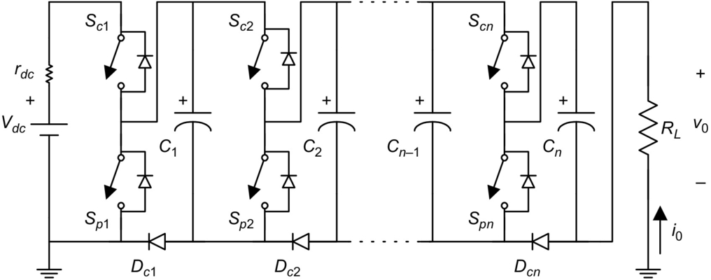
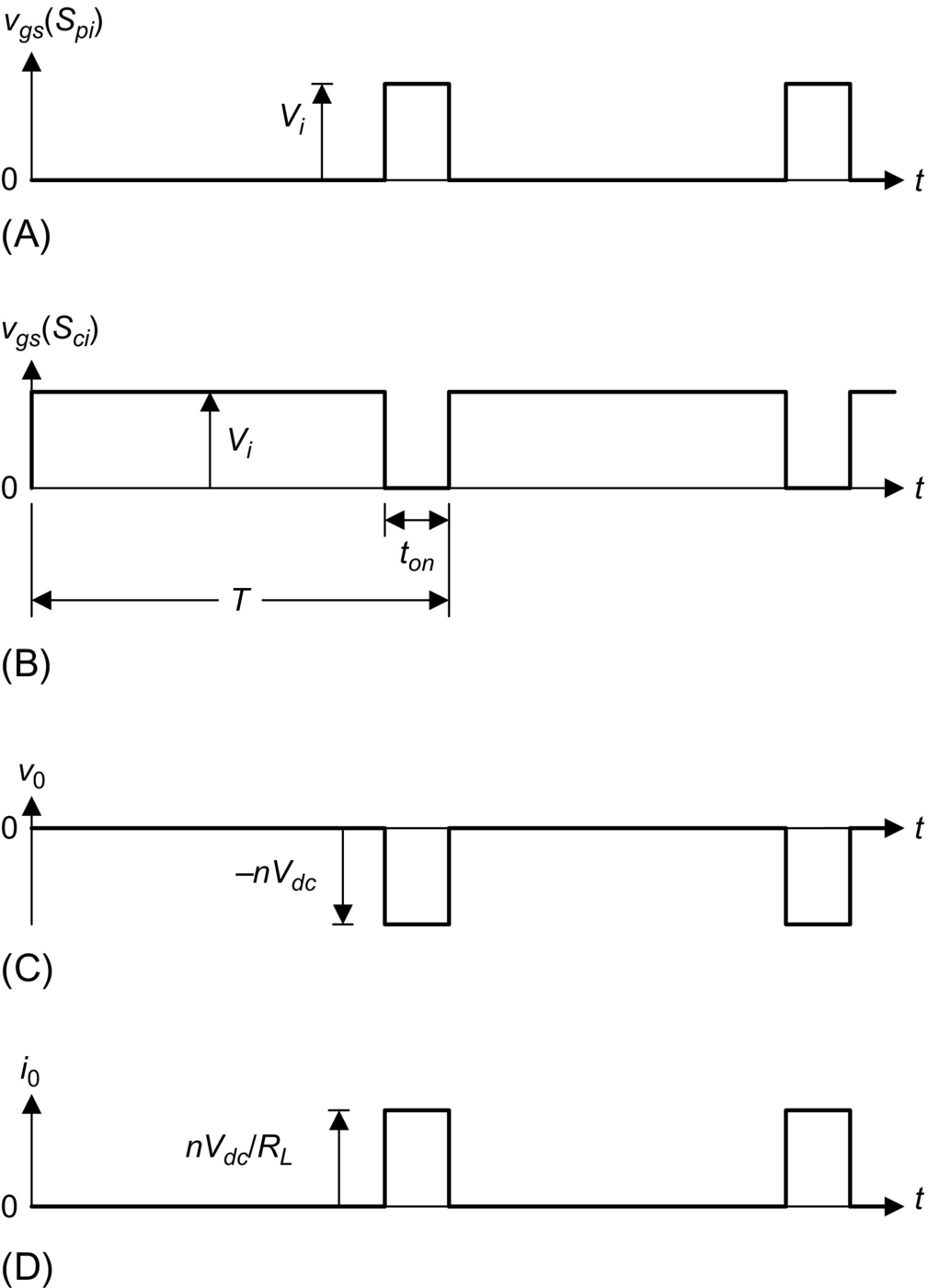
Considering resistive load, RL, the operation of the Fig. 18.45 modulator can be understood considering two operating modes, for a switch duty ratio D=ton/T. In the first one, switches Sci and Spi are, respectively, turned on and turned off. During the charging period, (T–ton), capacitors Ci are charged from the dc charging power supply, Vdc, with current limited by the internal resistance of the semiconductors, the wires, and the dc charging power supply internal resistance (or externally added) Rdc, resulting in a small time constant that enables kHz operation. The on-state of Dci ensures that during this period, the voltage, V0, applied to the load is, approximately, zero.
In the second operating mode, switches Sci and Spi are, respectively, turned off and turned on. During the pulse mode, ton, capacitors Ci are connected in series and their voltage applied to the load. The load voltage v0 is proportional to the charging power supply:
where n is the number of stages and k<1 characterizes the nonideal behavior of the passive and active elements in the circuit and operating conditions.
The Dci diodes guarantee, also, that the Spi switches only block a maximum voltage of Vdc, even in fault condition, such as the lack of synchronization. Considering Fig. 18.45, for example, if switch Tpn is off during pulse mode, Dcn conducts and short-circuits the last stage, imposing an output voltage of
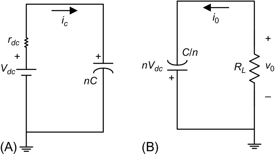
The operation of Fig. 18.45 circuit can be represented by its equivalent model during both operating modes, considering ideal switches and Ci=C. During the charging mode, the Ci capacitors are in parallel, and the circuit can be model as shown in Fig. 18.47A, where nC is the equivalent capacitance, seen by the power supply, charged with Vdc. In addition, during pulse mode, the Ci capacitors are in series, where C/n is the equivalent capacitance, seen by the load, charged with nVdc, as shown in Fig. 18.47B.
The energy stored in the Ci capacitors, during T–ton, is
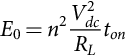
and the energy delivered to the load, during ton, is
For pulse power applications, only a small fraction of the stored energy should be transferred to the output during the pulse mode, otherwise the pulse voltage has a typical RC discharge waveform, not an almost rectangular shape. Considering a resistive load RL, the capacitance of the Ci capacitors in Fig. 18.45 circuit can be determined according to energy delivered to the load. For the required pulse voltage droop,

where ![]() is the capacitor voltage at the end-of-pulse mode, ton, and
is the capacitor voltage at the end-of-pulse mode, ton, and ![]() is the capacitors voltage immediately before pulse mode. Considering Eq. (18.101), the difference between Eqs. (18.99) and (18.100) is the energy stored in the Ci capacitors at end-of-pulse mode,
is the capacitors voltage immediately before pulse mode. Considering Eq. (18.101), the difference between Eqs. (18.99) and (18.100) is the energy stored in the Ci capacitors at end-of-pulse mode, ![]() :
:
where Eq. (18.102) for this case results in
Assuming that ![]() , equating (18.103), the capacitor value should satisfy the condition
, equating (18.103), the capacitor value should satisfy the condition
Considering Eqs. (18.99) through (18.104), it is mandatory to have storage energy greater than five times the pulse energy in order to have an output voltage droop better than 10%, but if a 1% voltage droop is expected, a 50 times storage energy is required, which impose limits to the design of the modulator.
The power dissipation in the switches and the capacitors charging time impose a high-voltage pulse frequency limitation. Therefore, this circuit operates better with low duty ratio, D, pulses as required in most PP applications.
In addition, the Vdc power supply must be able to charge the Ci capacitors with an energy equal to the delivered pulse energy, E0, plus losses during the charging time, T–ton:
where the Ploss term represents the power dissipated in the circuit wiring and switches.
This determines the maximum power rating for the Vdc power supply that imposes the maximum operating frequency, pulse duty ratio, and load power to the modulator.
To build and operate the circuit of Fig. 18.45, some design consideration must be considered. First, during start-up, when the energy storing capacitors are completely discharged, the charging voltage Vdc must be slowly increased in order to limit the charging current on the switches Sci and Dci, which is critical in the first stages due to the parallel charging topology of the capacitors.
Actually, in the parallel charging method, the semiconductor modules current loading is not equal. For instance, in the Fig. 18.45 circuit, switch Sc1 conducts current required to capacitors C1, C2…, Cn–1, Cn, switch Sc2 conducts charging current for C2, C3…, Cn–1, Cn, and so forth. Thus, in practical implementation, modules with successive decreasing current ratings can be used, the benefits of standardization being somewhat compromised.
Also, the Sci and Spi switches conduct different current values, respectively, the discharge and pulse current. Hence, instead of switches needing to block unequal voltages, they are required to conduct unequal currents.
Consequently, when choosing semiconductors to implement the S switches, it is fundamental that the semiconductor current rating must be selected to guarantee that the devices work always in the saturation region inside the forward safe operating area. If not, during the first instants of the on-state (when the current is high) the semiconductors can operate in the active region where the voltage drop and losses are higher, which might destroy the devices.
The switches triggering is another important concern in these circuits. There are two drive signals, vgs(Spi) and vgs(Sci), respectively, to Spi and Sci, which should be triggered synchronously. Since all the semiconductor switches are at different high-voltage potentials, gate drive circuits with galvanic isolation are required (the use of optical fibers is mandatory to transmit the gate signals and to reduce stray capacitances to ground and neighbor cells), together with isolated power supplies to further process the transmitted gate signal and supply power to the gate drivers.
Several authors have come up with solutions to supply power to semiconductor triggering drivers for high-voltage applications. The most common include isolation transformers [59], but diode strings are also described [57].
The circuit in Fig. 18.45 enables the use of typical half-bridge semiconductor structures currently integrated in modular packages, which is advantageous to assemble the circuit and trigger the semiconductors, since it allows bootstrap operation [10].
However, the circuit topology shown in Fig. 18.45 is not suitable for dealing with capacitive loads. In fact, if a capacitive-type load is connected to the circuit output, the load stays charged after the HV pulse with a negative voltage until the charging mode of the energy storing capacitors. However, during the charging period, the load is not shorted by the Dci, except if the energy stored in the load is very low and the charging current of capacitors Ci is sufficient to turn-on diodes Dci.
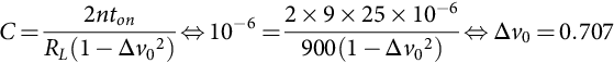
In order to guarantee the discharge of the load capacitances after the negative HV pulse, it is necessary to change the Fig. 18.45 circuit topology for the one shown in Fig. 18.48, which also produces negative HV pulses into the load.

Considering the circuit in Fig. 18.48, as the Vdc power supply is negative, it is necessary to change the topology in comparison with Fig. 18.45 in order to maintain a similar operating behavior. The two main differences are the addition of an extra switch, Sc0, which guarantees that during the pulse period, the dc charging power supply Vdc does not participate in the pulse mode, ton. The most important regards the fact that during the charging period, T–ton, the Sci switches short-circuit the load discharging any capacitance, as the one shown in Fig. 18.48.
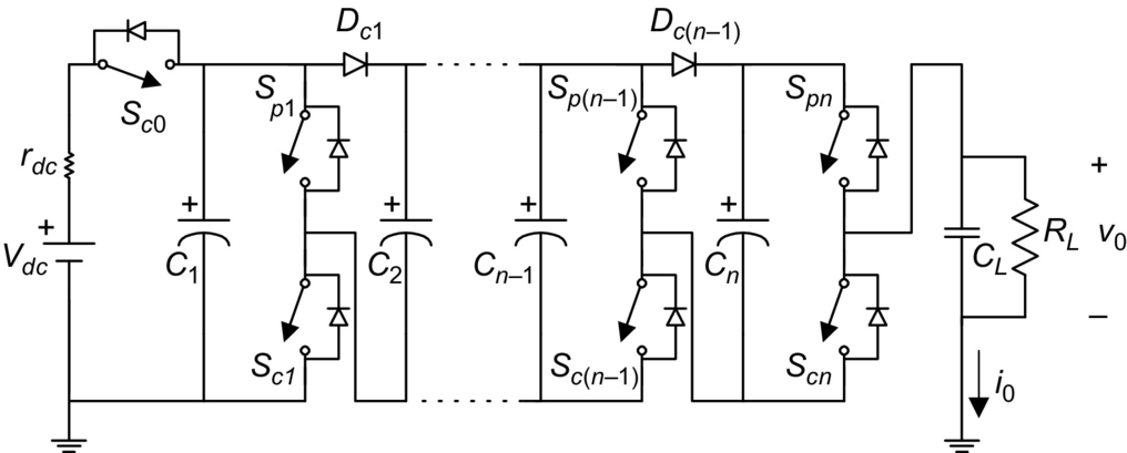
Considering now the application of negative HV pulses into inductive loads, the circuit in Fig. 18.45 requires an additional half-bridge switching structure that connects to the load, as shown in Fig. 18.49.
As shown in Fig. 18.50, the operation of the circuit in Fig. 18.49 in comparison with circuit of Fig. 18.45, has some changes, which includes one additional time period for enabling the reset of the inductive load by the freewheeling diodes, Tab, besides the charging, Tc, and pulse modes, ton, in order to impose a zero average voltage to the load.
During the charging period, the on-state of Dci and the Sp(n+1) antiparallel diode ensures that the output voltage, V0, applied to the load is approximately zero.
After the HV negative pulse, ton, the Sci and Spi switches are turned off, but in order to conserve energy, the inductive load current, i0, must have an alternative path. This path is set by freewheeling diodes (Sci antiparallel diodes and Dci diodes) and the capacitor with the lowest voltage, which is charged. Normally, Cn has the lowest voltage; thus, the current path is through the Sc(n+1) antiparallel diode DB, capacitor Cn, and diodes Dc1–Dcn. During this time, Ta, the voltage applied to the load is, about, Vdc (voltage in capacitor Cn), resetting the inductive load. Capacitor Cn is charged until its voltage is equal to the capacitor Cn–1 voltage, after which, if there is still energy in the load, the current path changes to capacitor Cn–1. As the maximum clamping voltage is Vdc, the higher the number of stages the longer the resetting time.
In this way, most of the load magnetic energy is sent back to energy storing capacitors Ci, after which the load current i0 goes to zero, and it can be imposed again the charging mode of operation. It is important to have a safety time tb in order to guarantee the completely reset of the load. Due to this load energy recovery method, the power supply energy needed to charge the capacitors after each pulse is lower, and the yield of this modulator can be higher.
Example 18.9
A negative solid-state Marx generator needs to be assembled for delivering −9 kV and 25 μs pulses into a 900 Ω resistive load, with less than 20% voltage droop. Considering the existing equipment, there are two alternatives: (1) Vdc=1.5 kV, n=6, and Ci=1 μF and (2) Vdc=1 kV, n=9, and Ci=1 μF. Determine which is the best alternative.
Solution
Considering the capacitance of 1 μF in each stage, then, the pulse voltage droop can be determined by Eq. (18.104). Hence, for the first alternative,

and for the second alternative,
which gives, respectively, 18.35% and 29.23% voltage droop, meaning that after the pulse the capacitors stay charged with about Eq. (18.101), respectively, 1224.7 and 707.1 V. Hence, only the first alternative keeps the pulse voltage droop below 20%. In this case, the energy stored in the capacitors is Eq. (18.99) 6.75 J, three times bigger than the energy delivered to the load during each pulse Eq. (18.100) 2.25 J.
18.4.4.2 Generation of Positive Pulses
The solid-state Marx modulators for generating positive HV pulses, with different load conditions, have equivalent properties as the ones for negative pulses, shown in the last section, besides the necessary modifications to enable the change in the output polarity. Thus, Fig. 18.51 shows the basic topology of the SM, with n stages, able to deliver positive high-voltage repetitive pulses into resistive and capacitive loads, RLCL.
During the pulse mode, ton, the switches Sci and Spi are, respectively, turned off and turned on. Capacitors Ci are connected in series and their voltage applied to the load. The load voltage v0 is proportional to the charging power supply:
where n is the number of stages and k<1 characterizes the nonideal behavior of the passive and active elements in the circuit and operating conditions. Also, in this topology, for example, if Spn is off during pulse mode, the antiparallel Scn diode conducts and short-circuits the last stage, imposing an output voltage of
Actually, the Fig. 18.51 circuit is equivalent to Fig. 18.45 circuit, whereas in this case with a positive Vdc power supply, it can produce positive HV pulses for both resistive and capacitive loads. The capacitive load can be driven, given that during the charging mode of capacitors Ci, the load is short-circuited by the Sci switches, stray inductances limiting the discharge rate.
Considering now the application of positive HV pulses into inductive loads, the circuit in Fig. 18.51 requires an additional switch Sp0 and diode D0 at the input, as shown in Fig. 18.52.
The circuit operation requires, also, an additional time period for resetting the inductive load by the added freewheeling diodes, tab, in addition to the charging, tc, and pulse modes, ton, in order to impose a zero average voltage to the load.
Considering an inductive load, after the HV positive pulse, the Sci and Spi switches are off, and the path for the inductive current i0 is set by the capacitor Cn, which usually has the lowest voltage, the Sci antiparallel diode and diode DB. During this time, the voltage applied to the load is approximately −Vdc (the voltage in capacitor Cn), resetting the inductive load. After the load current i0 goes to zero, the charging mode of operation can be imposed.
18.4.5 Solid-State Marx-Based High-Voltage Switches
The solid-state Marx generator concept described in the last section can be used for distributing the voltage in series-stacked semiconductors. Further, the Marx generator circuit can be used as a series switch, maintaining some intrinsic properties, which are desirable for the use with relatively low-voltage semiconductors, such as equal voltage distribution between stages and the fact the semiconductors in each stage hold off only the stage voltage capacitor.
The Marx series switch, based on the solid-state Marx of Fig. 18.51, for positive voltages, is shown in Fig. 18.53 not to apply voltage but to hold it between its terminals. Therefore, the input power supply Vdc is removed, and the Spi switches are replaced by diodes Dpi. Also, resistors Rci are connected in parallel with the Dci diodes in order to balance the voltage in the capacitors Ci.
Consider the common HV pulse power topology of Fig. 18.54, where switches S1 and S2 commutate alternately. A HV power supply, Vdc, charges an energy storage capacitor Cdc, with current limited by resistor Rdc. The switch S1 applies the capacitor Cdc voltage vc to the capacitive load CL||RL, during the pulse period, ton. Subsequently, switch S2 discharges the load and other circuit parasitic capacitances to zero.

Taking into account the proposed operating scheme, each switch Si, where i∈{1, 2}, holds a maximum voltage equal to the power supply voltage amplitude, Vdc, considering that the capacitor Cdc is charged with the voltage Vdc. When S1 is conducting, S2 holds off the voltage Vdc, and when S2 is conducting, S1 holds off the voltage Vdc. Hence, if the voltage Vdc is greater than a couple of kV, a solid-state switch comprising series-stacked semiconductors is mandatory for implementing switches S1 and S2.
The switching frequency of S1 and S2 and the pulse on time depend on the energy stored in the Cdc capacitor, on the load consumption, and on the power dissipated in the switches during commutation.
The proposed PP topology in Fig. 18.54 implemented with the series switch of Fig. 18.53 as series switch S1 (Marx 1) and S2 (Marx 2) is shown in Fig. 18.55.

The operation of Fig. 18.55 circuit can be understood considering the concept presented in Fig. 18.53 and the voltage waveforms presented in Fig. 18.57. For the first operating mode, during time ton, the Sci switches in Marx 1 are on, the Ci capacitors in Marx 1 are in parallel, and the Sci switches in Marx 2 are off, as shown in Fig. 18.56A. The capacitor Cdc voltage, vc, is applied into the load, v0, and the Ci capacitors in Marx 2 are stacked in series, through the Dpi diodes, distributing the voltage across the Sci switches, in parallel with the load.

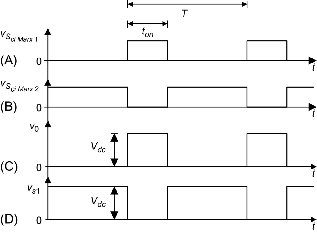
Subsequently, in the second operating mode, during time T–ton, the Sci switches in Marx 1 are off and the Sci switches in Marx 2 are on, and the load is discharged to zero, as shown in Fig. 18.56B. The vc voltage appears between the Marx 1 terminals as shown in Fig. 18.57D, where this voltage is sustained by the Ci capacitors in series through the Dpi diodes, distributing the voltage across the Sci switches.
Unlike in a typical Marx generator, the Ci capacitors in both Marx 1 and Marx 2 of Fig. 18.55 can suffer from voltage imbalance problems due to the fact that the Ci capacitors are charged in series: (i) in Marx 1 during period T–ton when the load is short-circuited and the voltage vC appears between the Marx 1 terminals, vS1, and (ii) in Marx 2 during period ton when the voltage is applied to the load and the voltage VC appears between the Marx 2 terminals.
Two main causes contribute to this voltage imbalance: (i) The Ci capacitance values are not equal, and (ii) the Ci capacitors placed near the Vdc power supply are charged with a higher voltage due to the voltage droop in the semiconductors in each stage. Considering the last, the Dci diodes do not conduct, and Rci are used in parallel to uniformly distribute the voltage between the Ci capacitors during (i) ton in the Marx 1 switch and (ii) T–ton in Marx 2 switch. Alternatively, extra switches can be placed in antiparallel with diodes Dci.
18.4.6 Solid-State Marx-Based Bipolar Generators
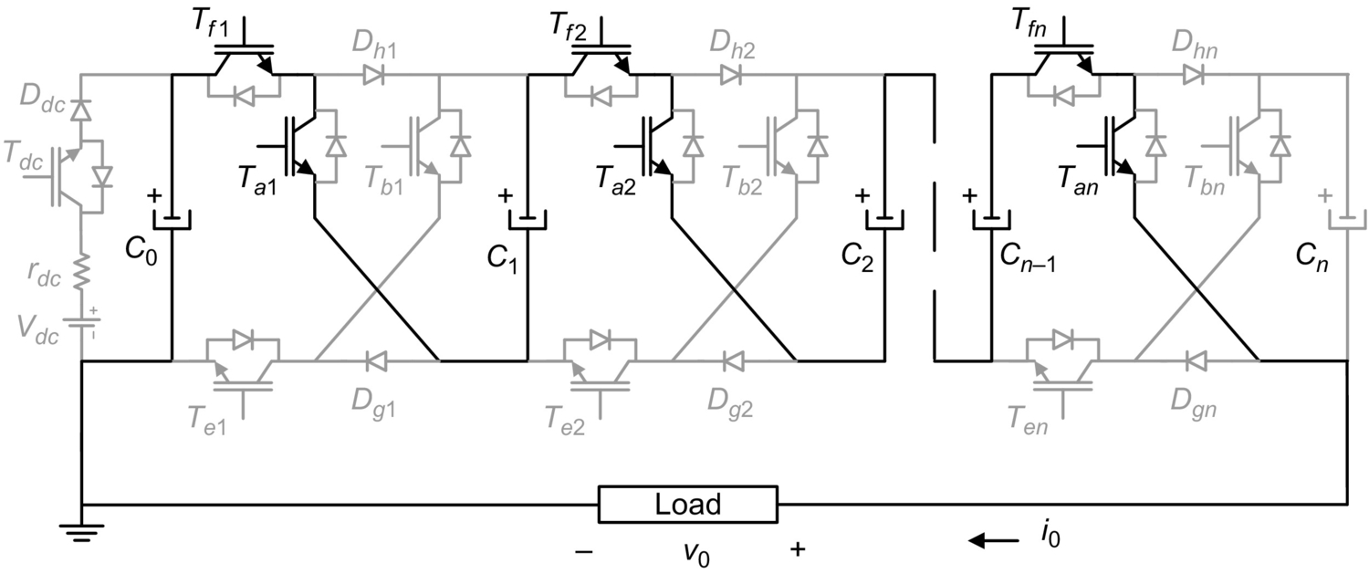
The Marx generator concept was extended in Ref. [60] to allow the generation of positive and/or negative pulses. This bipolar Marx generator is shown in Fig. 18.58, based in n modules with four controlled semiconductors Tfi, Tei, Tai, Tbi, (i∈{1,2,…,n}), two diodes Dhi, Dgi, and energy storage capacitor Ci.

During the charging period, the dc power supply Vdc charges the Ci capacitors in parallel from the power supply and C0 capacitor by turning ON switches Tdc, Ddc, Tfi, and Tei, through diodes Dhi and Dgi (Fig. 18.59). The on-state of Tei and Dgi switches, during this period, may guarantee a near-zero value to the load voltage, V0, provided the charging current is bigger than the load current.

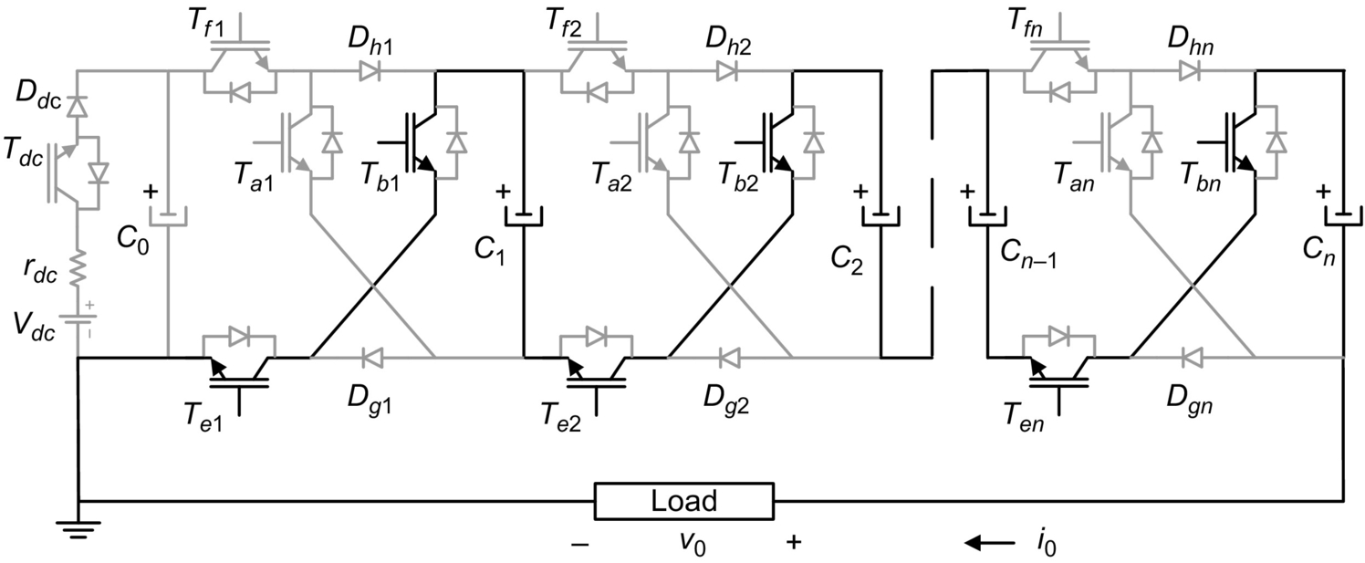
To obtain positive pulses, only switches Tfi and Tai are driven on (Fig. 18.60). For negative pulses, only switches Tbi and Tei are driven on (Fig. 18.61).
18.4.7 Solid-State Marx-Based Multilevel Bipolar Generators
Some of the previous presented Marx modulators may be used to generate staircase like voltage waveforms with multiple voltage levels, which can be useful to reduce electromagnetic interference since the rate of change of the pulse voltage is reduced regarding the two level voltage pulse.
The solid-state Marx-based high-voltage switch of Fig. 18.55 can be enhanced by adding an antiparallel transistor to diodes Dpi, to obtain one of the 2(n−1) modules of the multilevel bipolar generator in Fig. 18.62A, able to output n voltage levels [61]. The extra transistor and the Dk-1,k module interconnecting diode enable a better control of the charge/discharge of the storage capacitors Ck, since they can be connected in series with the capacitors in other modules to charge/discharge, or in parallel with some other capacitors to balance their voltages Fig. 18.62B, provided diode Dk-1,k is forward-biased [61].
The Ck capacitors are charged in series (being UCk≈Udc/(n−1)).
Considering a boolean switching function γk, the voltage Uk of each module is written as

Neglecting parasitic voltage drops, the load pulse voltage ULoad is

Supposing UCA=UCB=Udc/2, summing and subtracting the two previous equations, it can be obtained:

To obtain the maximum output voltage ULoadmax=Udc/2, it must be  , which from the second equation of (18.110) means
  . Supposing balanced capacitor voltages, then, each capacitor voltage is
 ![]() . To generate the minimum voltage, ULoadmin=−Udc/2, and then,
. To generate the minimum voltage, ULoadmin=−Udc/2, and then, 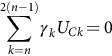 , being
  . These relationships show that each generator half arm must hold off the high-voltage Udc. From
 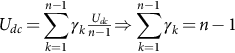 , which must be used to define the γk values needed for each level n. This means that half of the total 2(n−1) modules must have γk=1, while the remaining half must have γk=0. The γk values can create redundant states that must be used to balance the Ck capacitor voltages [61].
Fig. 18.63 shows the simulated output voltage of a seven levels (500 V each) 12 modules bipolar generator, including the zero voltage level.
18.5 Power Electronics in Capacitor Charging Applications
18.5.1 Introduction
Conventional dc power supplies operate at a given dc output voltage into a constant or near-constant load. However, pulse loads such as lasers, flashlamps, rail guns, and radar require short but intense bursts of energy. Typically, this energy is stored in a capacitor and then released into the load. The rate at which the capacitor is charged and discharged is called the repetition rate, T, and may vary from 0.01 Hz for large capacitor banks to a few kHz for certain lasers. Recharging the capacitor voltage to a specified voltage is tasked to a capacitor charging power supply (CCPS). The role of power electronics devices, topologies, and charging strategies for capacitor charging applications is presented in this chapter.
Fig. 18.64 shows the voltage across the energy storage capacitor connected to the output of a CCPS. This figure shows that the CCPS has three modes of operation. The first mode is the charging mode in which the capacitor is charged from an initial voltage of zero to a specified final voltage. The duration of the charging mode is determined by the capacitance of the energy storage capacitor and the rate at which the CCPS delivers energy. The next mode of operation is the refresh mode, which can be considered a “standby mode,” where the stored energy is simply maintained. When the output voltage drops below a predetermined value, the CCPS should turn-on and deliver the energy necessary to compensate for capacitor leakage. Since energy is lost during the refresh mode, the duration of the refresh mode should be as brief as possible. Issues that lead to nonzero refresh times include safety margins for worst-case charging and discharging mode times and SOA requirements of switching devices. The final mode of operation is the discharge mode in which the load is actively discharging the capacitor. The CCPS does not supply any energy to the load in this mode. The amount of time the CCPS remains in this mode is determined by how quickly the load can discharge the capacitor.

The instantaneous output power for a CCPS varies over a wide range in comparison to a conventional dc power supply that supplies a near-constant power to its load. This is shown in Fig. 18.65; the output power for the PP load is drawn as linear for illustration purposes only. The charging mode is characterized by high peak power. At the beginning of this mode, the output power is zero (i.e., there is no voltage present but current is flowing). Thus, the load capacitor is equivalent to a short-circuit. In addition, at the end of the charging mode, the output power is again zero (i.e., there is an output voltage present but no current is flowing). Now, the load capacitor is equivalent to an open-circuit. The refresh mode is typically a low-power mode because the current required to compensate for capacitor leakage is small. The CCPS does not supply any power during the discharge mode when the energy storage capacitor is being discharged by the pulsed load.

The average output power for a CCPS depends on the discharge mode energy and the repetition rate of the load. It is maximum when the energy storage capacitor is discharged at the end of the charging mode (large voltage and current), which corresponds to operation without a refresh mode. Because the CCPS power is not constant, the rating of a CCPS is often given in kJ/s instead of kW. The kJ/s rating can be written as
where WLOAD is the energy delivered to the load per charging cycle and T is the repetition rate. In the optimum case with no refresh and instantaneous discharge, the kJ/s rating is limited to how fast a particular capacitor can be charged by its specified voltage.
18.5.2 High-Voltage dc Power Supply With Charging Resistor
In this technique, the energy storage capacitor is charged by a high-voltage dc power supply through a charging resistor as shown in Fig. 18.66. The charging mode ends when the capacitor voltage equals the output voltage of the power supply. The capacitor is continually refreshed by the power supply. During the discharge mode, the charging resistor isolates the power supply from the pulse load. The advantages of this technique are its simplicity, reliability, and low cost.

The major disadvantage of this technique is its poor efficiency. In the charging mode, the energy dissipated in the charging resistor is equal to the energy stored in the capacitor in the ideal case; therefore, the maximum efficiency is 50%. As a result, this technique is utilized only in applications where the charge rate is low, that is, 200 J/s. Another disadvantage of this technique is related to the charging time, which is determined by the RC time constant. Some laser applications require that the output voltage be within 0.1% of a target voltage. For this technique, more than five time constants are required for the capacitor voltage to meet this voltage specification.
18.5.3 Resonance-Charging
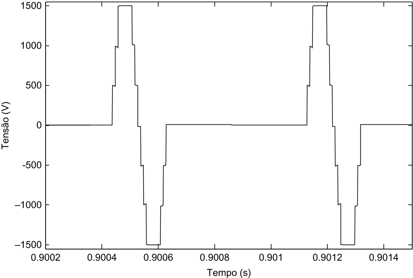
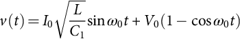
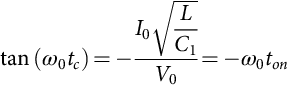
The basic resonance-charging technique is shown in Fig. 18.67. An ac input voltage is stepped up with a transformer, rectified, and filtered with capacitor C2 to produce a high dc voltage V0. In this circuit, C2 is much greater than C1. Thyristor T1 is gated and current flows through the inductor and diode D1 is transferring energy from C2 to C1. The voltage v(t) and current i(t) are described by the following equations assuming that ![]() . The charge time, tc, for this circuit can be calculated by finding the time at which the current, described by Eq. (18.112), reaches zero and is given below. The voltage v(t) has a value of 2V0 at the end of the charging mode:
. The charge time, tc, for this circuit can be calculated by finding the time at which the current, described by Eq. (18.112), reaches zero and is given below. The voltage v(t) has a value of 2V0 at the end of the charging mode:
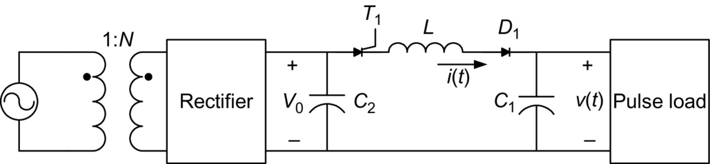
Even though this technique is simple and efficient, it is not without its limitations. A high-voltage capacitor with a large capacitance value is needed for C2, which increases the cost. A single thyristor is shown in Fig. 18.67. Multiple thyristors connected in series or a thyratron may be required depending on the voltage level. The repetition rate of the pulse load should be such that C1 is fully charged and i(t) has reached zero before the load discharges to prevent latch up of T1. It is not possible for this circuit to operate in the refresh mode because of the switch characteristics; therefore, v(t) will drift due to capacitor leakage. The charge time is a function of the circuit parameters and will drift as they change with temperature or due to aging.
Because all of the energy stored in C1 is transmitted from C2 in a single pulse, it can be difficult to achieve precise voltage regulation with the resonance-charging technique. However, regulation can be improved with the addition of a dequeing circuit as shown in Fig. 18.68. The voltage v(t) is monitored with a sensing network. Before v(t) reaches the desired level, thyristor T2 is fired, which terminates the charging mode. The remaining energy stored in the inductor is dissipated in R. The addition of the dequeing circuit reduces the circuit efficiency and increases the circuit complexity and cost but still does not enable a refresh mode to compensate for capacitor leakage.

Boost charging, a variation on the resonance-charging technique, is shown in Fig. 18.69 [62]. An extra switch is added to the circuit of Fig. 18.67, allowing energy to be stored in both C2 and L. This can be modeled as an increase in the voltage gain of the CCPS. With switches S1 and S2 closed, the current i(t) is given by

When ![]() , S2 is opened, and the current is now described by
, S2 is opened, and the current is now described by

where
is the inductor current initial value at ton. The voltage v(t) is then
The time required for the current to reach zero and for the voltage v(t) to reach its peak value can be calculated from
This is also the charge time, tc, or the length of the charging mode. Note from Eq. (18.119) that the charge time depends on ton, which is the on-time of switch S2. In addition, the peak capacitor voltage is a function of ton. The peak capacitor voltage is limited to 2V0 without S2; voltage gains as high as 20 are possible with the addition of S2 [62].
The switching elements in Figs. 18.67 and 18.68 are realized with thyristors. Simple switches are shown for the boost charging technique in Fig. 18.69. Switch S1 could be implemented with a thyristor. The boost capability provided by switch S2 is best realized with a gate-controlled semiconductor device such as a GTO or an IGBT.
18.5.4 Switching Converters
The poor efficiency when charging a capacitor through a resistor from a high-voltage power supply limits its application to low charging rates. In the resonance-charging concepts, the energy is transferred to the load capacitor in a single pulse, and it is not possible to compensate for capacitor leakage. Energy storage capacitors may be charged utilizing the same power electronic technology that has been applied in switching converters for constant power loads. Instead of charging the energy storage capacitor with a single pulse, switching converters can charge the capacitor with a series of pulses or pulse train. The peak current is reduced when charging with a series of pulses, thus improving the efficiency of the charging process. In addition, soft-switching techniques may be used in the switching converter to increase the efficiency. The regulation of the output voltage is also improved with the pulse train because the energy is passed to the energy storage capacitor as small packets. Common control techniques such as pulse width modulation can be used to control the size of the energy packet. This capability to control the size of the energy packet permits the CCPS to operate in the refresh mode and compensate for capacitor leakage. As a result, the CCPS may operate over a broad range of load repetition rates and still maintain tight output voltage regulation during refresh mode. During the refresh mode, energy lost due to capacitor leakage may be replaced in a burst fashion [63] or in a continuous fashion similar to trickle charging a battery [64].
In the switching converter, semiconductor switches may be operated on the lower side of the transformer permitting the use of MOSFETs or IGBTs in the CCPS. Because the CCPS begins the charging mode with a short-circuit across its output, the switching converter must be capable of operating under this severe load condition. This may require the implementation of a current limiting scheme in the converter control circuit.
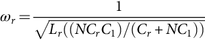
One switching converter as shown in Fig. 18.70 consists of a resonant converter. Note that the MOSFETs and resonant components Lr and Cr are connected on the low-voltage side of the transformer. Only the rectifier diodes and energy storage capacitor must have high-voltage ratings. When the output rectifier is conducting, the energy storage capacitor C1 is connected in series with the resonant capacitor Cr. For a transformer turn ratio of 1/N, reflecting C1 through the transformer yields a capacitance of N2C1. Since N is typically large, this reflected capacitance is much larger than Cr, thus the resonant frequency, which is defined in Eq. (18.120), is not affected by C1. For high-voltage, high-frequency operation, the leakage inductance of the transformer may be utilized as Lr. Thus, the resonant frequency can be expressed as
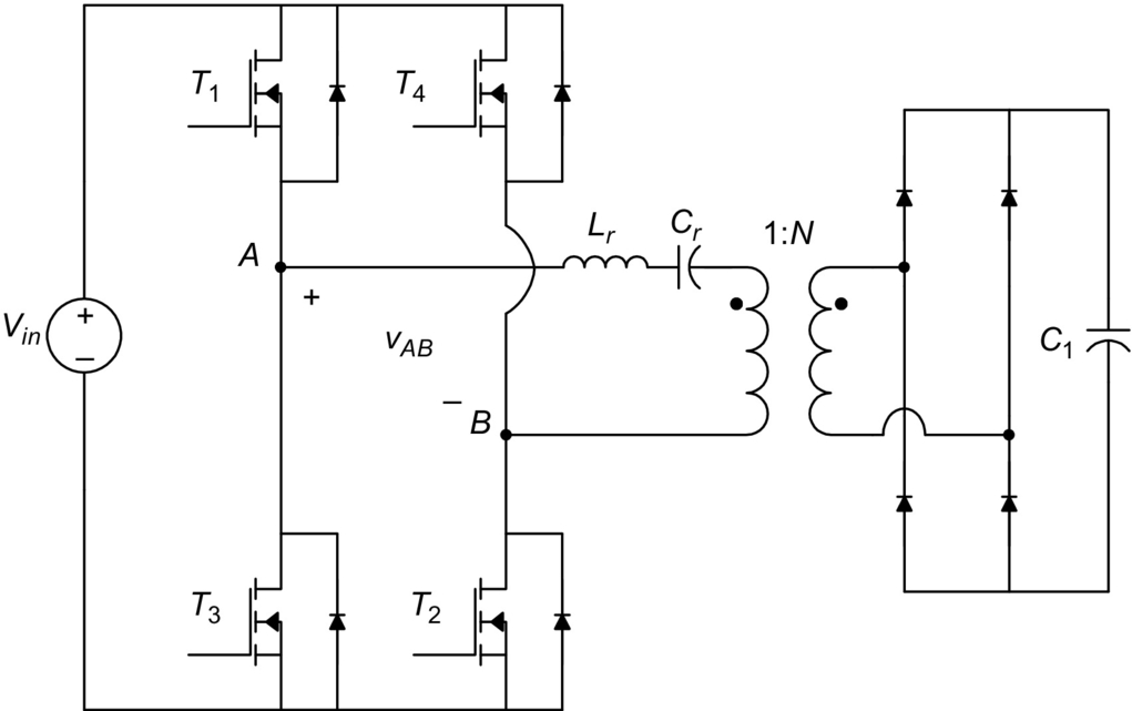
One characteristic of this converter, which makes it attractive for capacitor charging, is the ability to operate under the short-circuit conditions present at the beginning of the charging mode. The voltage across C1 is zero at the beginning of this mode. The current in the switches is limited by the input voltage and impedance Z0 as is defined in Eq. (18.121).

Another method for current limiting is to vary the ratio of fs, the switching frequency of the MOSFETs, and the resonant frequency, fr, which is ωr/2π. This effectively controls the flow of energy from the source to C1. The ratio fs/fr may be set to a low value at the beginning of the charging mode and increased toward unity as the voltage across C1 increases. This limits the current when the voltage across C1 is low and allows increased energy transfer as the voltage approaches the target voltage. The disadvantage of this approach is that variable frequency operation complicates device and component selection and degrades EMI/EMC performance of the CCPS.
The flyback converter, shown in Fig. 18.71, also may be utilized for capacitor charging applications [65,66]. When the MOSFET is turned on, current increases in the primary winding, storing energy in the magnetic field. When it reaches a specified level, the MOSFET is turned off and the energy is transferred from the magnetic field to C1. This energy transfer is terminated when the MOSFET is turned on again.

In cases where precise output regulation is not required and the packet energy is low, the diode in Fig. 18.71 can be replaced with a Zener diode with a Zener voltage of
where VO,nom is the nominal value of VO [67]. Once VO,nom is reached, the next energy packet will force the diode into a brief period of breakdown with the excess energy partially recycled to the input circuit. If the packet energy is small enough, the breakdown is not destructive and VO is limited to
where VO,Ω is the small excess voltage caused by the last energy packet.
Sokal and Redl [68] have investigated different control schemes for charging capacitors using the flyback converter. Their recommendation is to charge C1 with current pulses that are nearly flat-topped. This strategy results in higher average current for a given peak current. The capacitor is charged faster because the charge delivered to it during a pulse is directly proportional to the average current. This desired pulse shape is achieved by turning on the MOSFET to terminate the transfer of energy to C1 soon after the MOSFET is turned off, which increases the switching frequency. When the primary current rises to a preset minimum level, the MOSFET is again turned off. This switching strategy is essentially hysteretic current mode control, in which the switch current is limited between two preset bounds.
Another converter for capacitor charging applications is the Ward converter [69–71] shown in Fig. 18.72. When the MOSFET is turned on, energy is stored in the inductor, and capacitor Ca transfers energy into the energy storage capacitor C1 and capacitor Cb. The energy stored in the inductor is transferred to Ca when the MOSFET is turned off. The leakage inductance of the transformer and Ca resonate producing a sinusoidal current that flows in the primary winding of the transformer and the MOSFET. When the primary current reaches zero and starts negative, the diode turns on, which allows the MOSFET to be turned off efficiently at zero-current.
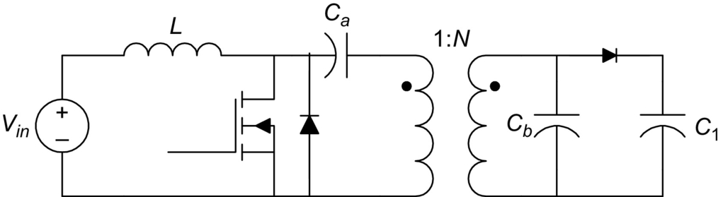
In some converter operating conditions, the voltage across Ca is very small because most of the energy has been transferred from Ca to C1. The energy stored in Ca may be too small to ensure zero-current turnoff of the MOSFET. In this case, the energy stored in Cb helps to ensure that the amplitude of the current is large enough for zero-current turnoff of this device.
18.6 Conclusions and Future Trends
This chapter reviewed some of the most typical semiconductors and topologies used for generating repetitive unipolar and bipolar high-voltage pulses based on semiconductor devices for various load conditions. These topologies have in common the techniques for limiting the high-voltage stress onto the power semiconductor switches, still relatively low-voltage devices, considering the tens of kV needed for pulse power applications. High-voltage techniques spread from the series (and parallel) stacks of semiconductors switches to generalized cascodes, passing through the modified dc-dc isolated converters for pulse generation and their cascade association, to the Marx-type solid-state generators topologies and Marx-derived bipolar generators.
With semiconductor-based generators, pulse power applications have expanded into many new fields such as material modification, environment protection, and biological and medical developments. The presented topologies can bring a completely new extent of capability in repetition rate, efficiency, lifetime, compactness, and portability.
In addition to the methods to generate high-voltage pulse, the performances of the semiconductor switches determine the performance of the pulse power generators. In this way, power semiconductor devices have made significant progress in both power capability and operation speed. Various semiconductor switching units have become commercially available and have been used in various pulse power applications. The most typical devices such as SOS diodes, GTOs, IGBTs MOSFETs, SIThs, and the emerging devices based on SiC or GaN technology, such as SiC MOSFETs, JFETs, cascode JFETs, IGBTs, and GaN E-HEMTs, were described. As the performance of SiC devices continues to improve, it is expected they will replace the existing switching Si devices in high-voltage applications, reducing the number of needed stages.
State-of-the-art HV pulse generators must use several stages to obtain the desired final high-voltage pulse: the first stage can use SCRs and start at 1–2 kV, and then, intermediate full-bridge resonant stage using IGBTs or full-bridge associations can boost this voltage to 4–10 kV, which is applied to HV high-frequency or pulse transformers to obtain 50–100 kV in the secondary. Diode polyphase rectifiers in the transformer secondary windings or saturated pulse transformers can boost the voltage roughly to 300 kV. If needed, a final stage using a SOS or SAS diode can boost the voltage up to 1 MV. Alternatively, other solutions such as solid-state Marx generators are being used, each Marx module operating at 2–10 kV (using SiC semiconductors or series stacks if needed). The required number of Marx modules should be minimized and arranged in shielded groups, the groups being connected to obtain the full HV generator. Droop voltage control and balancing may be necessary to design a practical HV pulse generator. Power generators based in existing power electronics converters are also used to charge capacitors for high-voltage pulse generators.
The future of solid-state pulse power is linked to the capability of making semiconductor-based high-voltage generators with better characteristics in compactness, weight, cost, efficiency, modularity, and portability, very important to deal with future applications near the consumer.