Inverters
Nimrod Vázquez Technological Institute of Celaya, Celaya, Mexico
Joaquín Vaquero López King Juan Carlos University, Madrid, Spain
Abstract
In this chapter, not only single-phase inverters in their voltage-, current-, and impedance-source alternatives but also the three-phase inverters in their voltage- and current-source configurations will be reviewed. The multilevel configurations are also described. Specifically, the topologies, the modulating techniques, and the control aspects oriented to standard applications are analyzed. The inverters are required in many applications, like adjustable speed drives (ASDs), uninterruptible power supplies, static var compensators, active power filters, flexible ac transmission systems, and grid-connected photovoltaic systems, which are only a few applications.
Keywords:
Voltage-source inverter; Current-source inverter; Impedance-source inverter; Multilevel inverter; Modulation techniques; Single-phase inverters; Three-phase inverters
11.1 Introduction
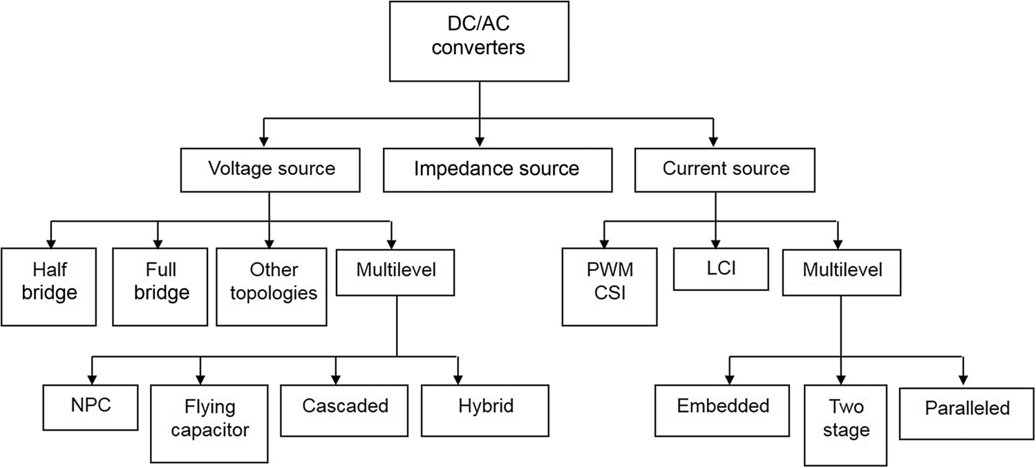
To produce an ac output waveform from a dc power supply is the main objective of inverters. These types of converters are required in many applications, like adjustable speed drives (ASDs), uninterruptible power supplies, static var compensators, active power filters, flexible ac transmission systems, and grid-connected photovoltaic systems, which are only a few applications. For sinusoidal ac outputs, the magnitude, frequency, and phase of the waveform should be controllable. In the literature, different topologies have been reported; one of the most known converters is the voltage-source inverters (VSIs), but current-source inverters (CSIs) and impedance-source inverters (ISIs) can also be found; in Fig. 11.1, a classification of inverters is illustrated that considers the input source. The VSIs are the most widely used because they naturally behave as voltage sources as required by many industrial applications, such as ASDs, which are the most popular application of inverters. Similarly, the other topologies are widely used in medium-voltage industrial or low-power commercial applications.
The inverters are constructed from power switches and diodes. This leads to the generation of waveforms that feature fast transitions rather than smooth ones. These waveforms are made up of a fundamental component that behaves as a pure sinusoidal and an infinite number of harmonics. This behavior should be ensured by a modulating technique that controls the amount of time and the sequence used to switch the power semiconductors on and off. The modulating techniques mostly used are the carrier-based technique (e.g., sinusoidal pulse width modulation, SPWM), the space-vector (SV) technique, and the selective harmonic elimination (SHE) technique.
As an alternative not only to produce an inverter output with low harmonic content but also to avoid the negative side effects of high dv/dt (such as bearing and isolation problems), the multilevel topologies should be used. The basic principle is to construct the required ac output waveform from various levels, which achieves waveforms at reduced dv/dt. Although these topologies are well developed in ASDs, they are also suitable for static var compensators, active power filters, and so on. Specialized modulating techniques have been developed to switch the higher number of power semiconductors involved in these topologies. Among others, the carrier-based (SPWM) and SV-based techniques have been naturally extended to these applications.
In many applications, it is required to take energy from the ac side of the inverter and send it back into the dc side. For instance, whenever ASDs need to either brake or slow down the motor speed, the kinetic energy is sent into the voltage dc link. This is known as the regenerative operating mode, and in contrast to the motoring mode, the dc link current direction is reversed due to the fact that the dc link voltage is fixed. If a capacitor is used to maintain the dc link voltage (as in standard ASDs), the energy must be either dissipated or fed back into the distribution system; otherwise, the dc link voltage gradually increases. The first approach requires the dc link capacitor be connected in parallel with a resistor, which must be properly switched only when the energy flows from the motor to the dc link. A better alternative is to feed back such energy into the distribution system. However, this alternative requires a reversible-current topology connected between the distribution system and the dc link capacitor. A modern approach to such a requirement is to use the active front-end rectifier technologies, where the regeneration mode is a natural operating mode of the system.
In this chapter, not only single-phase inverters in their voltage-, current-, and impedance-source alternatives but also the three-phase inverters in their voltage- and current-source configurations will be reviewed. Specifically, the topologies, the modulating techniques, and the control aspects oriented to standard applications are analyzed. In order to simplify the analysis, the inverters are considered lossless topologies, and the dc link will be assumed to be a perfect dc. Nevertheless, some practical nonideal conditions are also considered.
11.2 Single-Phase Inverters
Single-phase inverters can be classified by its input source; they are VSIs, CSIs, and ISIs. The operating principles are different in each converter. The main features of the different approaches are reviewed and presented in the following subsections. Although these converters cover the low-power range, they are widely used in power supplies or single-phase UPSs.
11.2.1 Voltage Source Inverter
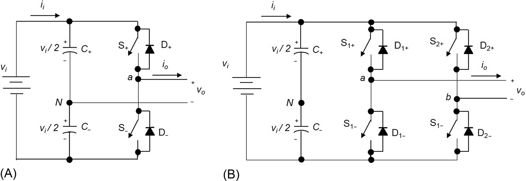
The traditional topologies for single-phase VSIs are half bridge and full bridge (Fig. 11.2). The converter is composed of capacitors, switches, and diodes, where an array of two switches is called “inverter leg.” For instance, the inverter leg of the half bridge is composed of S+![]() and S−
and S−![]() . The capacitors required to provide a neutral point N are large, such that each capacitor maintains a constant voltage.
. The capacitors required to provide a neutral point N are large, such that each capacitor maintains a constant voltage.
In order to operate properly the voltage-source inverter, the following rules are compulsory:
1. Switches of the same leg cannot be on simultaneously, because a short circuit across the dc link voltage source vi would be produced.
2. Diode in antiparallel to each switch must be placed, in order to provide a current path for inductive loads. If the commercial switch includes this diode, then the circuit is already complete.
3. In practical implementation, a dead time, also known as blanking time, must be considered in the control signals of the leg switches, to avoid breaking rule 1.
For the half-bridge VSI (Fig. 11.2A), there are two defined (states 1 and 2) and one undefined (state 3) switching state as shown in Table 11.1. In order to avoid an undefined ac output voltage condition, state 3 should be used just for the dead time. Then, the modulating technique should always ensure that at any instant either the top or the bottom switch of the inverter leg is on.
Table 11.1
Switch states for a half-bridge single-phase VSI
| State | State no. | vo | Components conducting | |
| S+ |
1 | vi/2 | S+ |
If io>0 |
| D+ |
If io<0 | |||
| S− |
2 | −vi/2 |
D− |
If io>0 |
| S− |
If io<0 | |||
| S+ |
3 | −vi/2 |
D− |
If io>0 |
| vi/2 | D+ |
If io<0 | ||

Fig. 11.3 shows the ideal waveforms associated with the half-bridge inverter shown in Fig. 11.2A. The states for the switches S+![]() and S−
and S−![]() are defined by the modulating technique, which in this case is a carrier-based PWM.
are defined by the modulating technique, which in this case is a carrier-based PWM.

 state, (C) switch S−
 state, and (D) ac output voltage.
For the full-bridge VSI (Fig. 11.2B), there are four defined (states 1–4) and one undefined (state 5) switching state as shown in Table 11.2. Again, in order to avoid an undefined ac output voltage condition, state 5 should be used just for the dead time. Then, the modulating technique should always ensure that at any instant either the top or the bottom switch of an inverter leg is on.
Table 11.2
Switch states for a full-bridge single-phase VSI
| State | State no. | vaN | vbN | vo | Components conducting | |
| S1+ |
1 | vi/2 | −vi/2 |
vi | S1+ |
If io>0 |
| D1+ |
If io<0 | |||||
| S1− |
2 | −vi/2 |
vi/2 | −vi |
D1− |
If io>0 |
| S1− |
If io<0 | |||||
| S1+ |
3 | vi/2 | vi/2 | 0 | S1+ |
If io>0 |
| D1+ |
If io<0 | |||||
| S1− |
4 | −vi/2 |
−vi/2 |
0 | D1− |
If io>0 |
| S1− |
If io<0 | |||||
| S1− |
5 | −vi/2 |
Depends on S2− |
D1− |
If io>0 | |
| vi/2 | D1+ |
If io<0 | ||||
| S2− |
vi/2 | Depends on S1− |
D2+ |
If io>0 | ||
| −vi/2 |
D2− |
If io<0 | ||||

Fig. 11.4 shows the ideal waveforms associated with the full-bridge inverter shown in Fig. 11.2B. The states for the switches are defined by the modulating technique, which in this case is a carrier-based PWM, but unipolar output is considered.
 state, (C) switch S2+
 state, and (D) ac output voltage.
For the VSIs, different output filters may be employed, in order to provide the fundamental component of the output. Depending on the application, it would be desirable to provide a voltage or a current output. In Fig. 11.5, some output filters for this converter are shown; in all cases, an inductor is required immediately for the output of the converter. The first and the last one are used to provide a current output, such as in VSIs connected to the grid, where a current-like performance is required. The second-order filter is used for voltage output, such as stand-alone applications or ASDs.

11.2.2 Current Source Inverter
The topology for the single-phase CSIs is the shown in Fig. 11.6. The converter is composed of inductors, switches, and diodes. The inductors required are large, such that the inductors maintain a constant current ii. Current-source topologies feature a low switching dv/dt and reliable overcurrent/short-circuit protection.
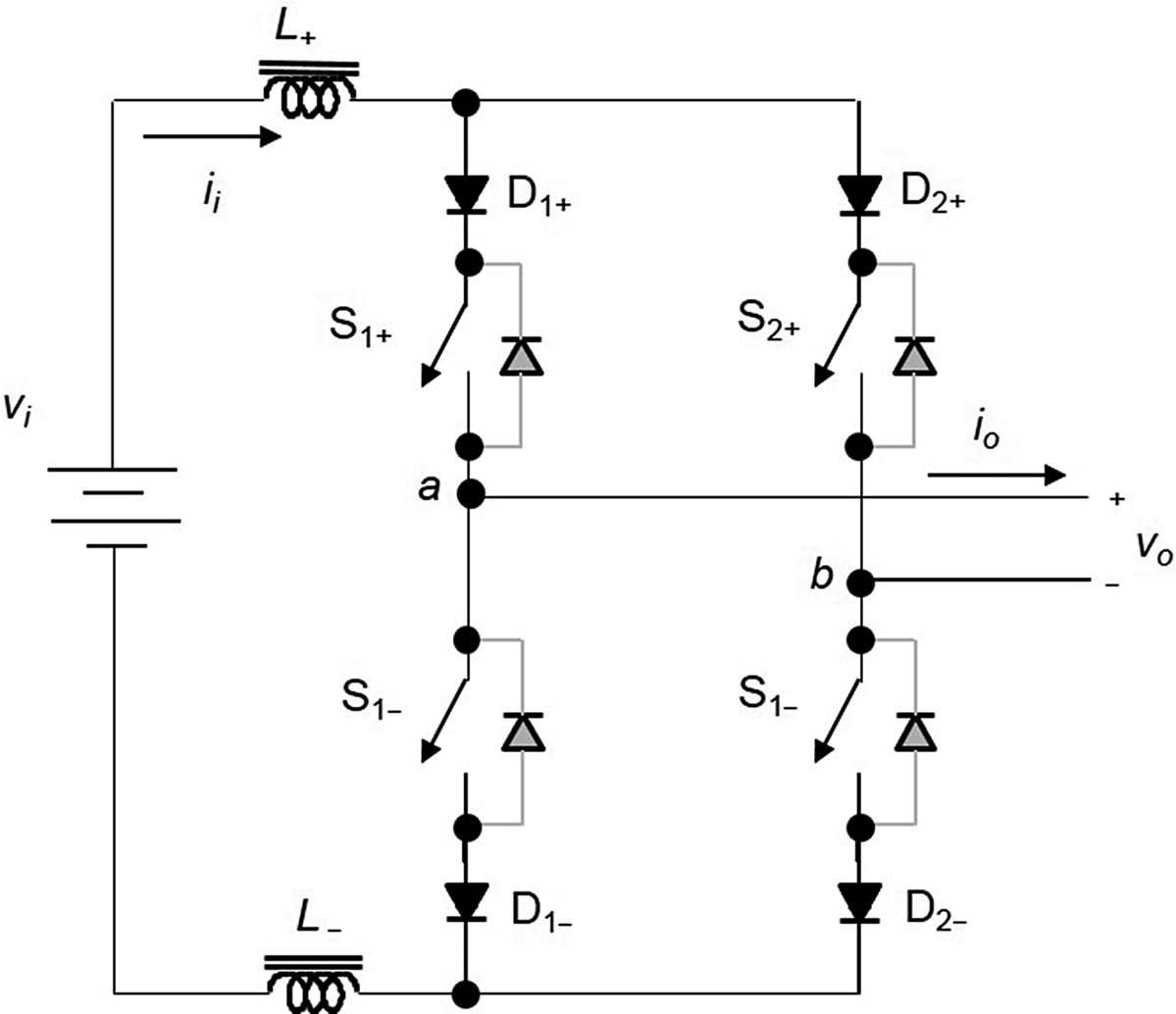
In order to operate properly the current-source inverter, the following rules are compulsory:
1. Top or bottom switches of the different legs cannot be off simultaneously, because no current path is provided to the input inductors.
2. Diode in series to each switch must be placed, because a short circuit across the output voltage vo would be produced. If the commercial switch does not include antiparallel diodes, then the circuit is already complete.
3. In practical implementation, an overlapping time must be considered in the control signals of the top or bottom switches of the different legs.
According to the previous rules, it should be noticed that both switches of the inverter leg can be turned on at the same time, and this is not possible in VSI.
For the CSI (Fig. 11.6), there are four defined (states 1–4) and one not permitted switching state (state 5) as shown in Table 11.3. The modulating technique should always ensure that at any instant, at least one of the top and bottom switch of the inverter legs is on; otherwise, the inverter will be damaged.
Table 11.3
Switch states for a single-phase CSI
| State | State no. | io | Components conducting |
| S1+ S1− |
1 | ii | S1+ D1+ |
| S1− S1+ |
2 | −ii | S1− D1− |
| S1+ S2+ |
3 | 0 | S1+ D1+ |
| S2+ S1+ |
4 | 0 | S2+ D1− |
| S1+ S2+ |
5 | This state must be avoided |
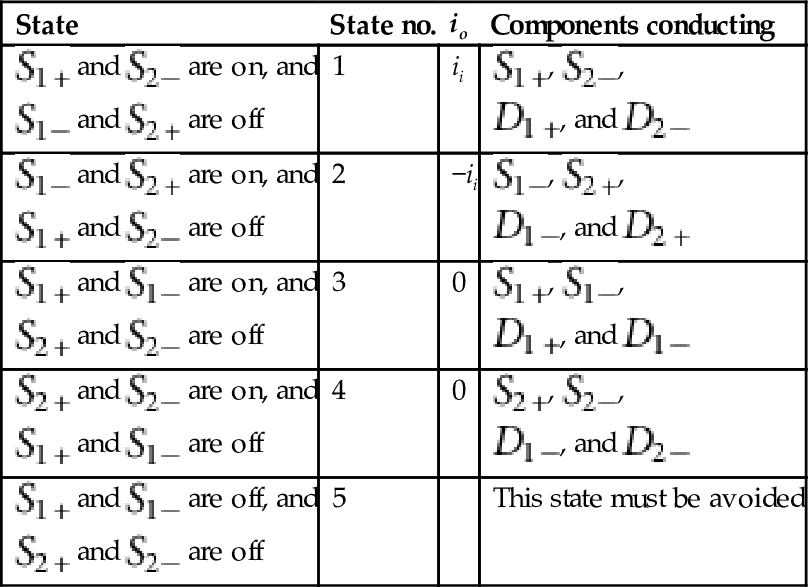
Fig. 11.7 shows the ideal waveforms associated with the CSI shown in Fig. 11.6. Notice that only the control signals of one inverter leg are graphed, since the other control signals are the opposite due to the rules (S1+![]() = not S2+
= not S2+![]() and S1−
and S1−![]() = not S2−
= not S2−![]() ), but the overlapping time should be considered for implementation. The states for the switches are defined by the modulating technique, which in this case is a carrier-based PWM, but unipolar output is considered.
), but the overlapping time should be considered for implementation. The states for the switches are defined by the modulating technique, which in this case is a carrier-based PWM, but unipolar output is considered.
 state, (C) switch S1−
 state, and (D) ac output current.
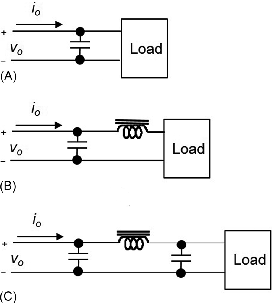
For the CSIs, different output filters may be employed, in order to provide the fundamental component of the output waveform. Depending on the application, it would be desirable to provide a voltage or current output. In Fig. 11.8, some output filters for this converter are shown; in all cases, a capacitor is required immediately for the output of the converter.
11.2.3 Impedance Source Inverter
There are different topologies for single-phase ISIs, namely, “Z,”- “qZ,”- and “TZ”-source inverters; in Fig. 11.9, the Z-source inverter (ZSI) is shown. The converter is composed of capacitors and inductors, switches, and diodes. The capacitors and the inductors are arranged to form an input impedance for the inverter.
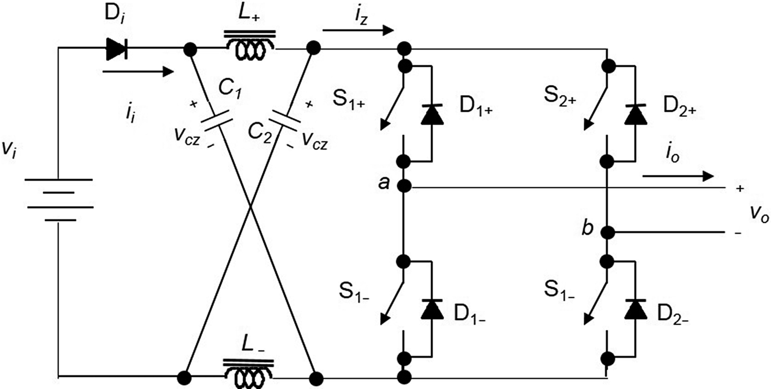
In order to operate properly the impedance-source inverter of Fig. 11.9, the following rules are compulsory:
1. No restrictions to the switches of the inverter leg apply.
2. Diodes in antiparallel to each switch must be placed, in order to provide a current path for inductive loads. If the commercial switch includes these diodes, then the circuit is already complete.
3. In practical implementation, no dead or overlapping time must be considered in the control signals of the leg switches.
According to the previous rules, it should be noticed that the switches of the inverter leg can be turned on and off at any time, and then, this converter has more switching states than the others, and this is used to boost the input voltage.
For the ISI shown in Fig. 11.9, there are five defined (states 1–5) and one undefined switching state as shown in Table 11.4. The modulating technique may permit to use the additional switching state (no. 5, known as shoot-through state), and then, another modulating signal should be employed for this purpose, but usually, it has a constant waveform.
Table 11.4
Switch states for a single-phase ZSI
| State | State no. | vo |
| S1+ |
1 | 2vcz−vi |
| S1− |
2 | −(2vcz−vi) |
| S1+ |
3 | 0 |
| S1− |
4 | 0 |
| S1+ |
5 | 0 |
| S1− | ||
| S1− |
6 | Depends on S2− |
| S2− |
Depends on S1− |

Fig. 11.10 shows the ideal waveforms associated with the ZSI shown in Fig. 11.9. The states for the switches are defined by the modulating technique, which in this case is a carrier-based PWM, but unipolar output is considered; the shoot-through state is modulated by vr.
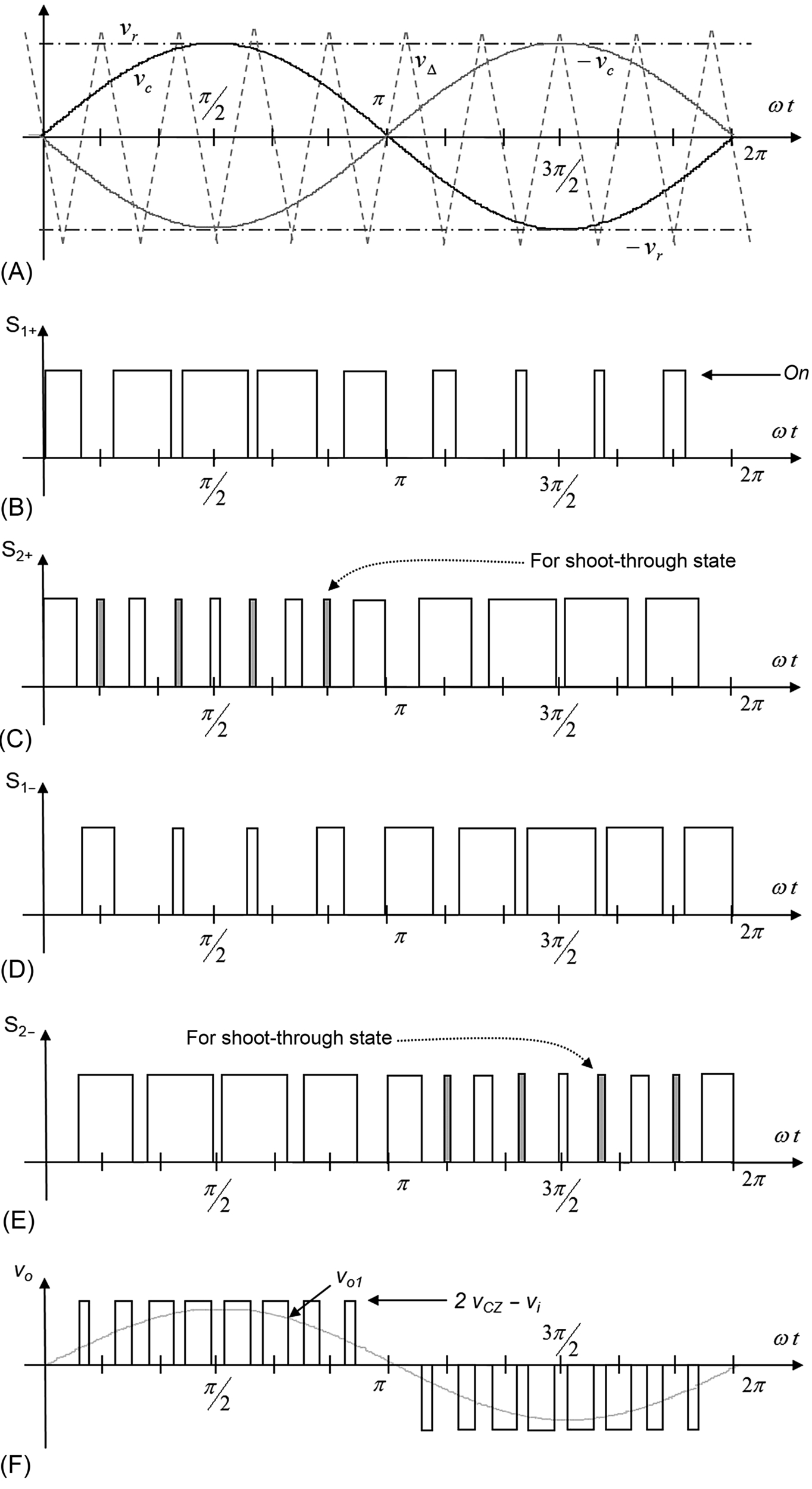 state, (C) switch S2+ state, (D) switch S1− state, (E) switch S2−
 state, and (F) ac output voltage.
For the converter ZSI, the output filter may be the same as for the VSI, and then, the filters are like the ones shown in Fig. 11.5.
11.2.4 Other Inverter Schemes
In the literature, other inverter topologies, with different operation from the previous discussed converters, have been proposed. However, the compulsory rules are valid, according to the input source. The entitled boost inverter is based on two bidirectional dc/dc boost converters and is able to produce an output voltage higher than the input voltage. This idea can be easily extrapolated to other dc/dc converter topologies. For more details, the appropriate references can be consulted.
11.2.5 Pulse Width Modulation
In order to produce a sinusoidal output, the pulse width modulation is employed. The modulating techniques mostly used are the carrier-based technique (e.g., sinusoidal pulse width modulation, SPWM), the space-vector (SV) technique, and the selective harmonic elimination (SHE) technique.
11.2.5.1 The Carrier-Based Pulse Width Modulation (PWM) Technique
As mentioned earlier, it is desired that the ac output voltage, vo, follows a given waveform (e.g., sinusoidal) on a continuous basis by properly switching the semiconductors. The carrier-based PWM technique fulfills such a requirement as it defines the on and off states of the switches of the inverter legs by comparing a modulating signal vc (desired ac output voltage) and a triangular waveform vΔ (carrier signal).
A special case is when the modulating signal vc is a sinusoidal at frequency fc and amplitude ˆvc![]() , and the triangular signal vΔ is at frequency fΔ and amplitude ˆvΔ
, and the triangular signal vΔ is at frequency fΔ and amplitude ˆvΔ![]() . This is the sinusoidal PWM (SPWM) scheme. In this case, the modulation index ma (also known as the amplitude modulation ratio) is defined as
. This is the sinusoidal PWM (SPWM) scheme. In this case, the modulation index ma (also known as the amplitude modulation ratio) is defined as
ma=ˆvcˆvΔ

and the normalized carrier frequency mf (also known as the frequency modulation ratio) is
mf=fΔfc

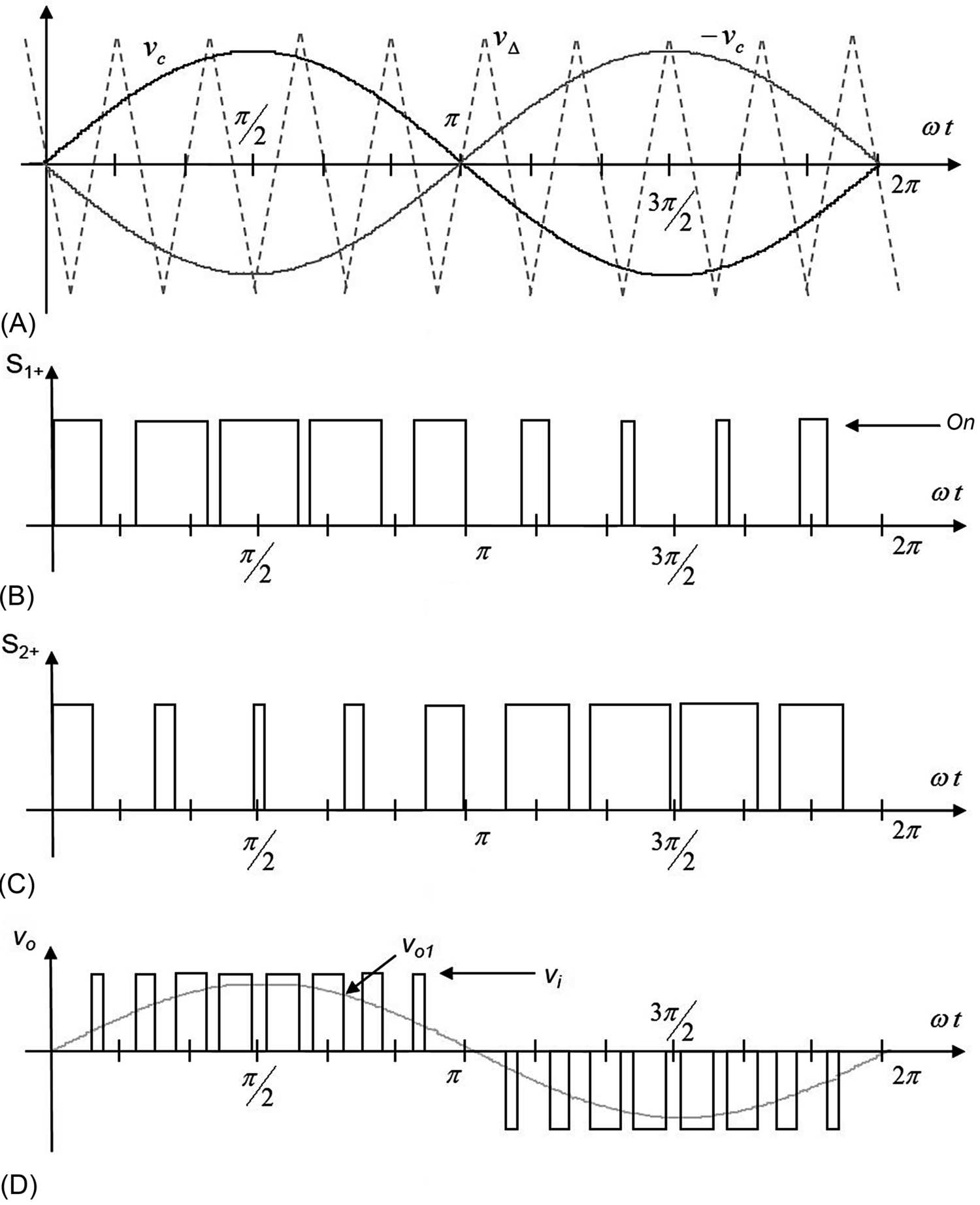
There are two known output waveforms entitled bipolar and unipolar output. Figs. 11.3D (bipolar) and 11.4d (unipolar) clearly show that the ac output voltage vo is basically a sinusoidal waveform plus harmonics.
Bipolar PWM technique
To generate a bipolar output, a carrier-based technique can be used as shown in Fig. 11.3. In this technique, only one modulating signal vc is used and also only one triangular signal vΔ. The important features for the bipolar output are the following:
(a) The amplitude of the fundamental component of the ac output voltage ˆvo1![]() satisfies the following expression:
satisfies the following expression:
ˆvo1=ˆvaN1=vi2ma
for half-bridge VSI, Fig. 11.2A,
ˆvo1=ˆvab1=vima
for the full-bridge VSI, Fig. 11.2B; these equations are valid for ma≤1![]() , which is called the linear region of the modulating technique (higher values of ma lead to overmodulation that will be discussed later).
, which is called the linear region of the modulating technique (higher values of ma lead to overmodulation that will be discussed later).
(b) For odd values of the normalized carrier frequency mf, the harmonics in the ac output voltage appear at normalized frequencies fh centered around mf and its multiples, specifically,
h=lmf±kl=1,2,3,…
where k=2,4,6,…![]() for l=1,3,5,…
for l=1,3,5,…![]() and k=1,3,5,…
and k=1,3,5,…![]() for l=2,4,6,…
for l=2,4,6,…![]() .
.
(c) The amplitude of the ac output voltage harmonics is a function of the modulation index ma and is independent of the normalized carrier frequency mf for mf>9![]() .
.
(d) The harmonics in the dc link current (due to the modulation) appear at normalized frequencies fp centered around the normalized carrier frequency mf and its multiples, specifically,
p=lmf±k±1l=1,2,…
where k=2,4,6,…![]() for l=1,3,5,…
for l=1,3,5,…![]() and k=1,3,5,…
and k=1,3,5,…![]() for l=2,4,6,…
for l=2,4,6,…![]() .
.
Additional important issues are the following: (a) For small values of mf (mf<21![]() ), the carrier signal vΔ and the signal vc should be synchronized to each other (mf integer), which is required to hold the previous features; if this is not the case, subharmonics will be present in the ac output voltage; (b) for large values of mf (mf>21
), the carrier signal vΔ and the signal vc should be synchronized to each other (mf integer), which is required to hold the previous features; if this is not the case, subharmonics will be present in the ac output voltage; (b) for large values of mf (mf>21![]() ), the subharmonics are negligible if an asynchronous PWM technique is used; however, due to potential very low-order subharmonics, its use should be avoided; finally, (c) in the overmodulation region (ma>1
), the subharmonics are negligible if an asynchronous PWM technique is used; however, due to potential very low-order subharmonics, its use should be avoided; finally, (c) in the overmodulation region (ma>1![]() ), some intersections between the carrier and the modulating signal are missed, which leads to the generation of low-order harmonics, but a higher fundamental ac output voltage is obtained; unfortunately, the linearity between ma and ˆvo1
), some intersections between the carrier and the modulating signal are missed, which leads to the generation of low-order harmonics, but a higher fundamental ac output voltage is obtained; unfortunately, the linearity between ma and ˆvo1![]() achieved in the linear region does not hold in the overmodulation region; moreover, a saturation effect can be observed (Fig. 11.11).
achieved in the linear region does not hold in the overmodulation region; moreover, a saturation effect can be observed (Fig. 11.11).

As mentioned before, the PWM technique allows an ac output voltage to be generated that tracks a given modulating signal. In the SPWM technique, the modulating signal is a sinusoidal that provides, in the linear region, an ac output voltage that varies linearly as a function of the modulation index, and the harmonics are at well-defined frequencies and amplitudes. These features simplify the design of filtering components. Unfortunately, the maximum amplitude of the fundamental ac voltage is bounded in this operating mode. Higher voltages are obtained by using the overmodulation region (ma>1![]() ); however, low-order harmonics appear in the ac output voltage. Very large values of the modulation index (ma>3.24
); however, low-order harmonics appear in the ac output voltage. Very large values of the modulation index (ma>3.24![]() ) lead to a totally square ac output voltage.
) lead to a totally square ac output voltage.
Unipolar PWM technique
To generate a unipolar output, also a carrier-based technique can be used as shown in Fig. 11.4, where two sinusoidal modulating signals (vc and −vc)![]() are used. The signal vc is used to generate S1+, and −vc
are used. The signal vc is used to generate S1+, and −vc![]() is used to generate S2+. Notice that this output cannot be produced by a half-bridge inverter. Important features for the unipolar output are the following:
is used to generate S2+. Notice that this output cannot be produced by a half-bridge inverter. Important features for the unipolar output are the following:
(a) The amplitude of the fundamental component of the ac output voltage ˆvo1![]() satisfies the following expression:
satisfies the following expression:
ˆvo1=2⋅ˆvaN1=ma⋅vi
(b) Since the phase voltages (vaN and vbN) are identical but 180° out of phase, the output voltage (vo=vab=vaN−vbN![]() ) will not contain even harmonics. Thus, if mf is taken even, the harmonics in the ac output voltage appear at normalized odd frequencies fh centered around twice the normalized carrier frequency mf and its multiples. Specifically,
) will not contain even harmonics. Thus, if mf is taken even, the harmonics in the ac output voltage appear at normalized odd frequencies fh centered around twice the normalized carrier frequency mf and its multiples. Specifically,
h=lmf±kl=2,4,…
where k=1,3,5,…![]() ; this feature is considered to be an advantage because it allows the use of smaller filtering components to obtain high-quality voltage and current waveforms while using the same switching frequency as in VSIs modulated by the bipolar approach.
; this feature is considered to be an advantage because it allows the use of smaller filtering components to obtain high-quality voltage and current waveforms while using the same switching frequency as in VSIs modulated by the bipolar approach.
(c) The amplitude of the ac output voltage harmonics is also a function of the modulation index ma.
(d) The harmonics in the dc link current appear at normalized frequencies fp centered around twice the normalized carrier frequency mf and its multiples. Specifically,
p=lmf±k±1l=2,4,…
where k=1,3,5,…![]()
11.2.5.2 Selective Harmonic Elimination
The main objective is to obtain a sinusoidal ac output voltage waveform where the fundamental component can be adjusted arbitrarily within a range and the intrinsic harmonics selectively eliminated. This is achieved by mathematically generating the exact instant of the turn-on and turnoff of the power semiconductors. The ac output voltage features odd half- and quarter-wave symmetry; therefore, even harmonics are not present (voh=0![]() , h=2,4,6,…
, h=2,4,6,…![]() ). Moreover, the phase voltage waveform (vo) should be chopped N times per half cycle in order to adjust the fundamental and eliminate N−1
). Moreover, the phase voltage waveform (vo) should be chopped N times per half cycle in order to adjust the fundamental and eliminate N−1![]() harmonics in the ac output voltage waveform.
harmonics in the ac output voltage waveform.
For this modulation, also the output may be bipolar or unipolar.
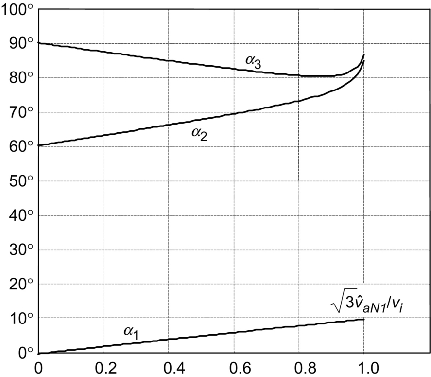
Bipolar SHE technique
The general expressions to eliminate an even N−1![]() (N−1=2,4,6,…
(N−1=2,4,6,…![]() ) number of harmonics are
) number of harmonics are
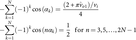
−N∑k=1(−1)kcos(αk)=(2+πˆvo1)/vi4−N∑k=1(−1)kcos(nαk)=12forn=3,5,…,2N−1
where α1, α2,…, αN should satisfy α1<α2<⋯<αN<π/2![]() .
.
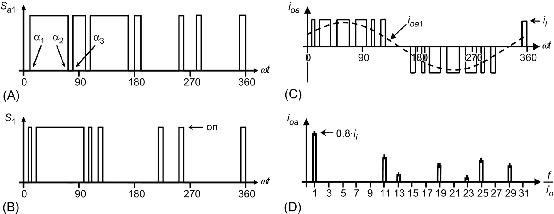
For instance, to eliminate the third and fifth harmonics and to perform fundamental magnitude control (N=3![]() ), the equations to be solved are the following:
), the equations to be solved are the following:
cos(1α1)−cos(1α2)+cos(1α3)=(2+πˆvo1/vi)/4cos(3α1)−cos(3α2)+cos(3α3)=1/2cos(5α1)−cos(5α2)+cos(5α3)=1/2

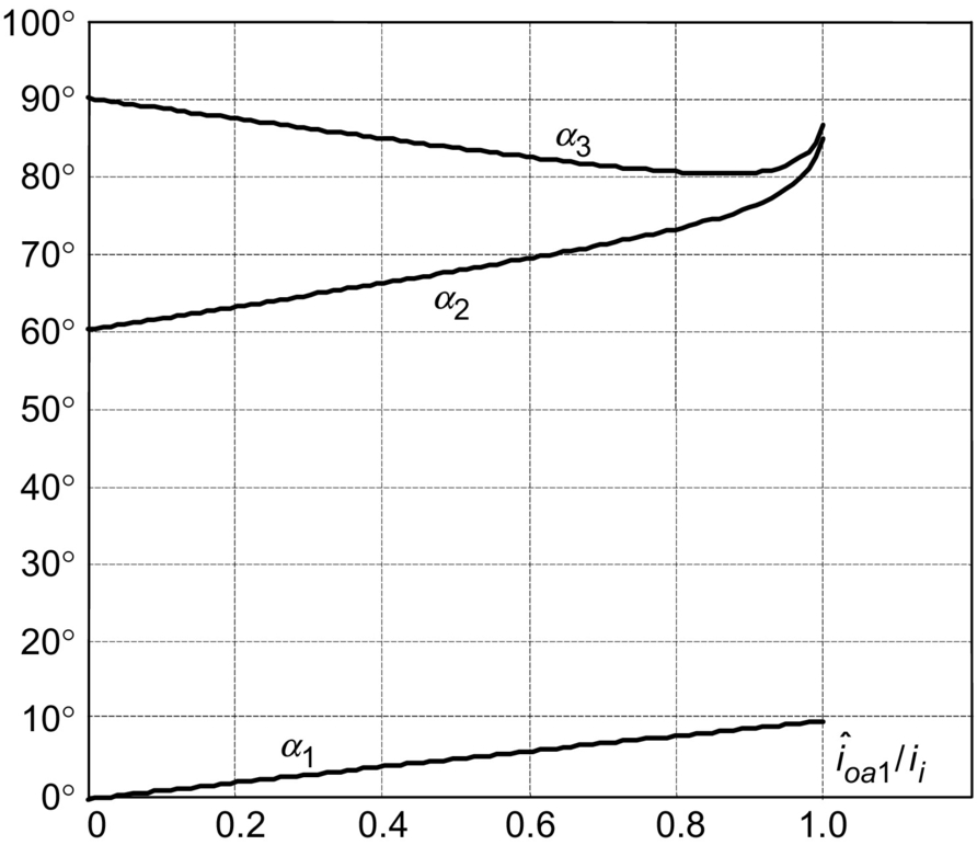
where the angles α1, α2, and α3 are defined as shown in Fig. 11.12A and the spectrum in Fig. 11.12B. The angles are found by means of iterative algorithms as no analytic solutions can be derived. The angles α1, α2, and α3 are plotted for different values of ˆvo1/vi![]() in Fig. 11.13A.
in Fig. 11.13A.


Similarly, the general expressions to eliminate an odd N−1![]() (N−1=3,5,7,…
(N−1=3,5,7,…![]() ) number of harmonics are given by
) number of harmonics are given by
−N∑k=1(−1)kcos(nαk)=(2−πˆvo1)/vi4−N∑k=1(−1)kcos(nαk)=12forn=3,5,…,2N−1

where α1,α2,…,αN should satisfy α1<α2<⋯<αN<π/2![]() .
.
For instance, to eliminate the third, fifth, and seventh harmonics and to perform the fundamental magnitude control (N−1=3![]() ), the equations to be solved are
), the equations to be solved are
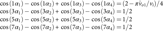
cos(1α1)−cos(1α2)+cos(1α3)−cos(1α4)=(2−πˆvo1/vi)/4cos(3α1)−cos(3α2)+cos(3α3)−cos(3α4)=1/2cos(5α1)−cos(5α2)+cos(5α3)−cos(5α4)=1/2cos(7α1)−cos(7α2)+cos(7α3)−cos(7α4)=1/2
where the angles α1, α2, α3, and α4 are defined as shown in Fig. 11.12C, and the spectrum in Fig. 11.12D. The angles α1, α2, and α3 are plotted for different values of ˆvo1/vi![]() in Fig. 11.13B.
in Fig. 11.13B.
Unipolar SHE technique
The general expressions to eliminate an arbitrary N−1![]() (N−1=3,5,7,…
(N−1=3,5,7,…![]() ) number of harmonics are given by
) number of harmonics are given by
−N∑k=1(−1)kcos(nαk)=π4(ˆvo1vi)−N∑k=1(−1)kcos(nαk)=0forn=3,5,…,2N−1

where α1,α2,…,αN should satisfy α1<α2<⋯<αN<π/2![]() .
.
For instance, to eliminate the third, the fifth, and the seventh harmonics and to perform fundamental component magnitude control (N=4![]() ), the equations to be solved are
), the equations to be solved are
cos(1α1)−cos(1α2)+cos(1α3)−cos(1α4)=πˆvo1/(vi4)cos(3α1)−cos(3α2)+cos(3α3)−cos(3α4)=0cos(5α1)−cos(5α2)+cos(5α3)−cos(5α4)=0cos(7α1)−cos(7α2)+cos(7α3)−cos(7α4)=0

where the angles α1, α2, α3, and α4 are defined as shown in Fig. 11.14A and the spectrum in Fig. 11.14B. The angles α1, α2, α3, and α4 are plotted for different values of ˆvo1/vi![]() in Fig. 11.15A.
in Fig. 11.15A.
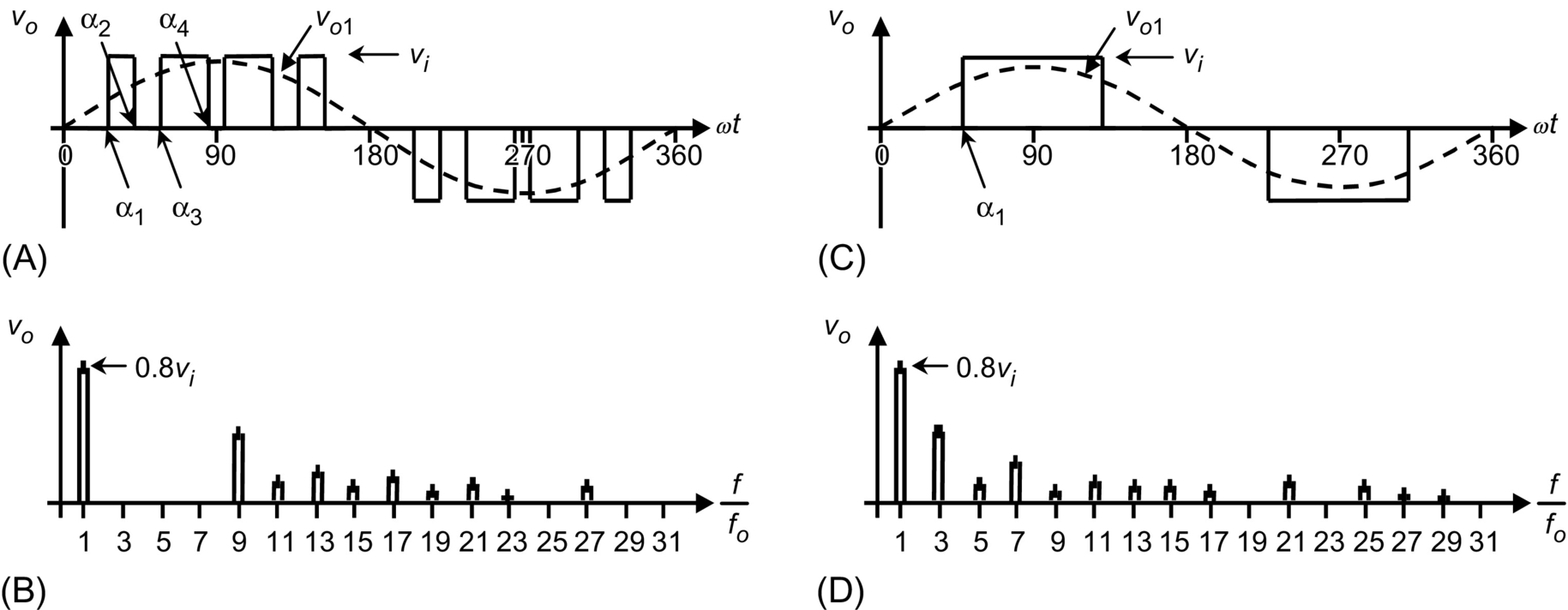

Fig. 11.14C shows a special case where only the fundamental ac output voltage is controlled. This is known as output control by voltage cancellation, which derives from the fact that its implementation is easily attainable by using two phase-shifted square-wave switching signals as shown in Fig. 11.16. The phase-shift angle becomes two ⋅α1![]() (Fig. 11.16B). Thus, the amplitude of the fundamental component and harmonics in the ac output voltage are given by
(Fig. 11.16B). Thus, the amplitude of the fundamental component and harmonics in the ac output voltage are given by
 state, (B) switch S2+ state, (C) ac output voltage, and (D) ac output voltage spectrum.
ˆvoh=4πvi(−1)(h−1)/2hcos(hα1)h=1,3,5,…

It can also be observed in Fig. 11.16C that for α1=0![]() square-wave operation is achieved. In this case, the fundamental ac output voltage is given by
square-wave operation is achieved. In this case, the fundamental ac output voltage is given by
ˆvo1=4πvi

where the fundamental load voltage can be controlled by the manipulation of the dc link voltage vi. Additional means to modify this voltage should be provided. Depending on the dc link source of power, this could be a controlled rectifier, for ac sources, or a dc/dc converter, for dc sources.
To implement the SHE modulating technique, the modulator should generate the gating pattern according to the angles as shown in Figs. 11.13 and 11.15. This task is usually performed by digital systems that normally store the angles in look-up tables.
11.2.5.3 DC Link Current
Due to the fact that the inverter is assumed lossless and constructed without storage energy components, the instantaneous power balance indicates that
vi(t)·ii(t)=vo(t)·io(t)
For inductive load and relatively high switching frequencies, the load current Io is nearly sinusoidal. As a first approximation, the ac output voltage can also be considered sinusoidal. On the other hand, if the dc link voltage remains constant vi(t)=Vi, Eq. (11.18) can be simplified to
ii(t)=1/Vi√2Vo1sin(ωt)·√2Iosin(ωt−φ)
where Vo1 is the fundamental rms ac output voltage, Io is the rms load current, and φ is an arbitrary inductive load power factor. Thus, the dc link current can be further simplified to
ii(t)=Vo1/ViIocos(φ)−Vo1/ViIocos(2ωt−φ)
The preceding expression reveals an important issue, that is, the presence of a large second-order harmonic in the dc link current (its amplitude is similar to the dc link current). This second harmonic is injected back into the dc voltage source; thus, its design should be considered in order to guarantee a nearly constant dc link voltage. In practical terms, the dc voltage source is required to feature large amounts of capacitance, which is costly and demands space, both undesired features, especially in medium- to high-power supplies.
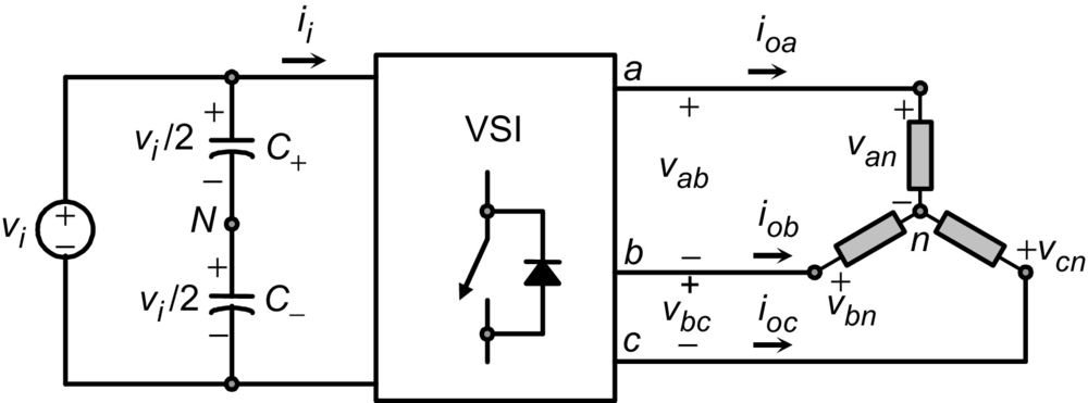
11.3 Three-Phase Voltage Source Inverters
Single-phase VSIs cover low-range power applications, and three-phase VSIs cover medium- to high-power applications. The main purpose of these topologies is to provide a three-phase voltage source, where the amplitude, phase, and frequency of the voltages should always be controllable. Although most of the applications require sinusoidal voltage waveforms (e.g., ASDs, UPSs, FACTS, and var compensators), arbitrary voltages are also required in some other applications (e.g., active power filters and voltage compensators).
The standard three-phase VSI topology is shown in Fig. 11.17, and the eight valid switch states are given in Table 11.5. As in single-phase VSIs, the compulsory rules previously described in Section 11.2.1 also apply.
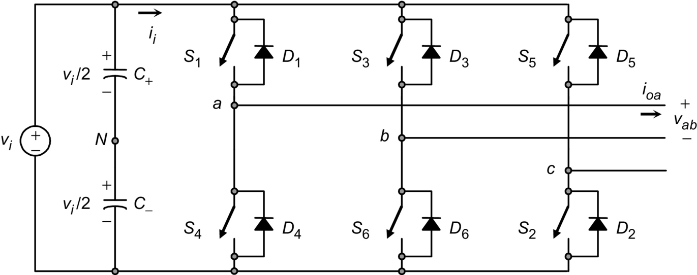
Table 11.5
Valid switch states for a three-phase VSI
| State | State no. | vab | vbc | vca | Space vector |
| S1, S2, and S6 are on, and S4, S5, and S3 are off |
1 | vi | 0 | −vi |
→v1=1+j0.577 |
| S2, S3, and S1 are on, and S5, S6, and S4 are off |
2 | 0 | vi | −vi |
→v2=j1.155 |
| S3, S4, and S2 are on, and S6, S1, and S5 are off |
3 | −vi |
vi | 0 | →v3=−1+j0.577 |
| S4, S5, and S3 are on, and S1, S2, and S6 are off |
4 | −vi |
0 | vi | →v4=−1−j0.577 |
| S5, S6, and S4 are on, and S2, S3, and S1 are off |
5 | 0 | −vi |
vi | →v5=−j1.155 |
| S6, S1, and S5 are on, and S3, S4, and S2 are off |
6 | vi | −vi |
0 | →v6=1−j0.577 |
| S1, S3, and S5 are on, and S4, S6, and S2 are off |
7 | 0 | 0 | 0 | →v7=0 |
| S4, S6, and S2 are on, and S1, S3, and S5 are off |
8 | 0 | 0 | 0 | →v8=0 |

Of the eight valid states, two of them (7 and 8 in Table 11.5) produce zero ac line voltages. The remaining states (1–6 in Table 11.5) produce nonzero ac output voltages. In order to generate a given voltage waveform, the inverter moves from one state to another. Thus, the resulting ac output line voltages consist of discrete values of voltages that are vi, 0, and −vi![]() for the topology shown in Fig. 11.17. The selection of the states in order to generate the given waveform is done by the modulating technique that should ensure the use of only the valid states.
for the topology shown in Fig. 11.17. The selection of the states in order to generate the given waveform is done by the modulating technique that should ensure the use of only the valid states.
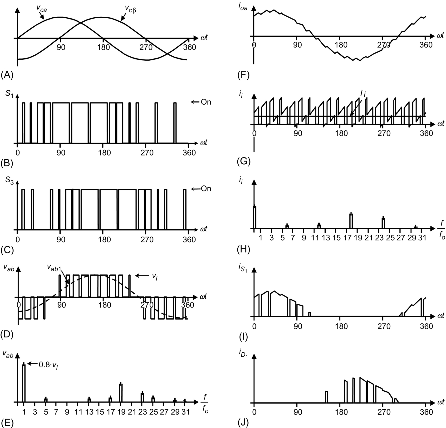
11.3.1 Sinusoidal PWM
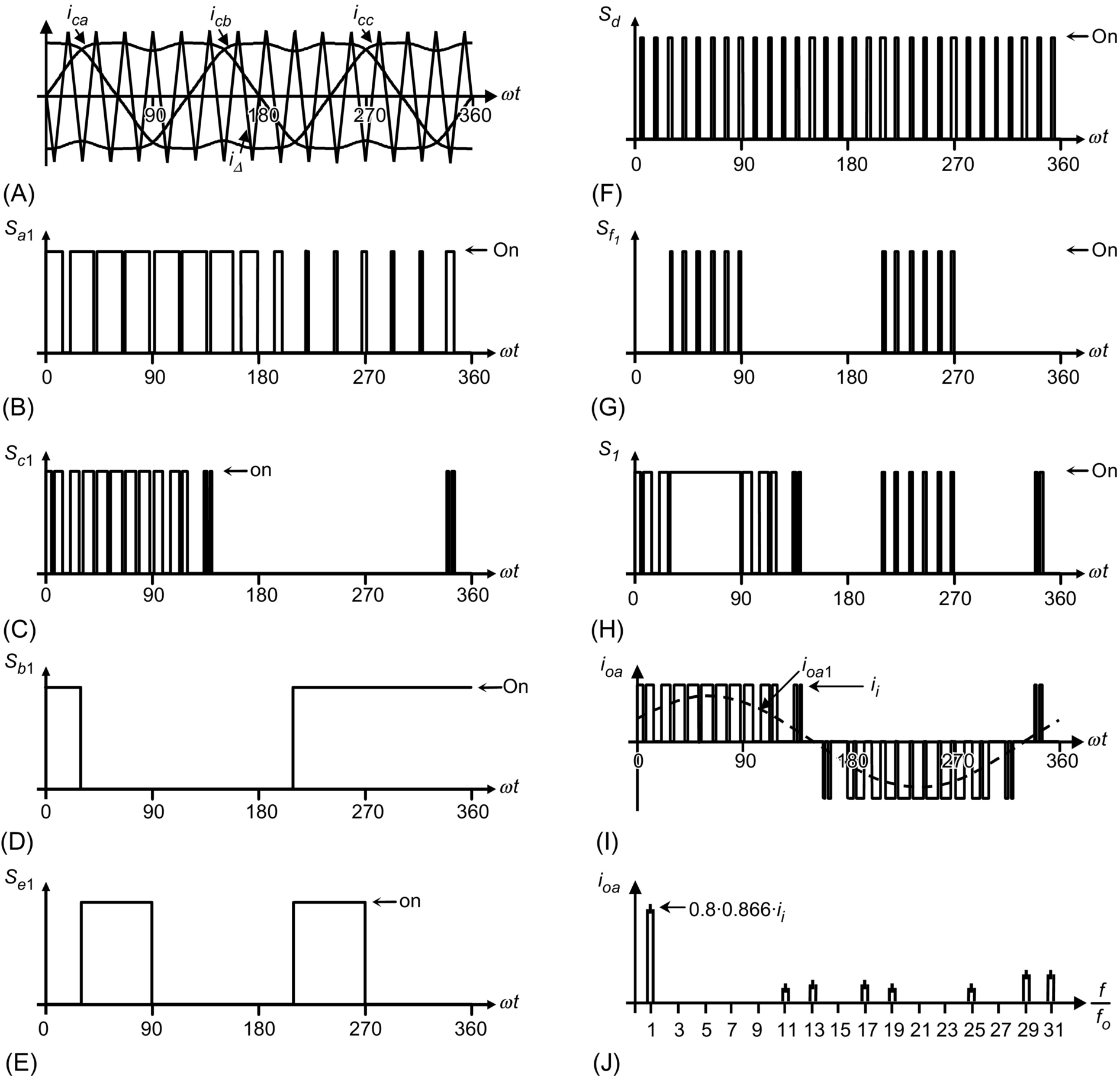
This is an extension of the one introduced for single-phase VSIs. In this case and in order to produce 120° out-of-phase load voltages, three modulating signals that are 120° out of phase are used. Fig. 11.18 shows the ideal waveforms of three-phase VSI SPWM. In order to use a single-carrier signal and preserve the features of the PWM technique, the normalized carrier frequency mf should be an odd multiple of 3. Thus, all phase voltages (vaN, vbN, and vcN)![]() are identical, but 120° out of phase without even harmonics; moreover, harmonics at frequencies, a multiple of 3, are identical in amplitude and phase in all phases. For instance, if the ninth harmonic in phase aN is
are identical, but 120° out of phase without even harmonics; moreover, harmonics at frequencies, a multiple of 3, are identical in amplitude and phase in all phases. For instance, if the ninth harmonic in phase aN is

 , mf=9
 ): (A) carrier and modulating signals, (B) switch S1 state, (C) switch S3 state, (D) ac output voltage, (E) ac output voltage spectrum, (F) ac output current, (G) dc current, (H) dc current spectrum, (I) switch S1 current, and (J) diode D1 current.
vaN9(t)=ˆv9sin(9ωt)
the ninth harmonic in phase bN will be
vbN9(t)=ˆv9sin[9(ωt−120°)]=ˆv9sin(9ωt−1080°)=ˆv9sin(9ωt)
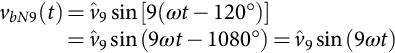
Thus, the ac output line voltage vab=vaN−vbN![]() will not contain the ninth harmonic. Therefore, for odd multiple of 3 values of the normalized carrier frequency mf, the harmonics in the ac output voltage appear at normalized frequencies fh centered around mf and its multiples, specifically, at
will not contain the ninth harmonic. Therefore, for odd multiple of 3 values of the normalized carrier frequency mf, the harmonics in the ac output voltage appear at normalized frequencies fh centered around mf and its multiples, specifically, at
h=lmf±kl=1,2,…
where l=1,3,5,…![]() for k=2,4,6,…
for k=2,4,6,…![]() and l=2,4,…
and l=2,4,…![]() for k=1,5,7,…
for k=1,5,7,…![]() such that h is not a multiple of 3. Therefore, the harmonics will be at mf±2
such that h is not a multiple of 3. Therefore, the harmonics will be at mf±2![]() , mf±4,…
, mf±4,…![]() , 2mf±1
, 2mf±1![]() , 2mf±5,…,3mf±2
, 2mf±5,…,3mf±2![]() , 3mf±4,…,4mf±1
, 3mf±4,…,4mf±1![]() , 4mf±5,…
, 4mf±5,…![]() . For nearly sinusoidal ac load current, the harmonics in the dc link current are at frequencies given by
. For nearly sinusoidal ac load current, the harmonics in the dc link current are at frequencies given by
h=lmf±k±1l=1,2,…
where l=0,2,4,…![]() for k=1,5,7,…
for k=1,5,7,…![]() and l=1,3,5,…
and l=1,3,5,…![]() for k=2,4,6,…
for k=2,4,6,…![]() such that h=l⋅mf±k
such that h=l⋅mf±k![]() is positive and not a multiple of 3.
is positive and not a multiple of 3.
The identical conclusions can be drawn for the operation at small and large values of mf as for the single-phase configurations. However, because the maximum amplitude of the fundamental phase voltage in the linear region (ma≤1![]() ) is vi/2, the maximum amplitude of the fundamental ac output line voltage is √3vi/2
) is vi/2, the maximum amplitude of the fundamental ac output line voltage is √3vi/2![]() . Therefore, one can write
. Therefore, one can write
ˆvab1=ma√3vi20<ma≤1
To further increase the amplitude of the load voltage, the amplitude of the modulating signal ˆvc![]() can be made higher than the amplitude of the carrier signal ˆvΔ
can be made higher than the amplitude of the carrier signal ˆvΔ![]() , which leads to overmodulation. The relationship between the amplitude of the fundamental ac output line voltage and the dc link voltage becomes nonlinear as in single-phase VSIs. Thus, in the overmodulation region, the line voltages range is
, which leads to overmodulation. The relationship between the amplitude of the fundamental ac output line voltage and the dc link voltage becomes nonlinear as in single-phase VSIs. Thus, in the overmodulation region, the line voltages range is
√3vi2<ˆvab1=ˆvbc1=ˆvca1<4π√3vi2
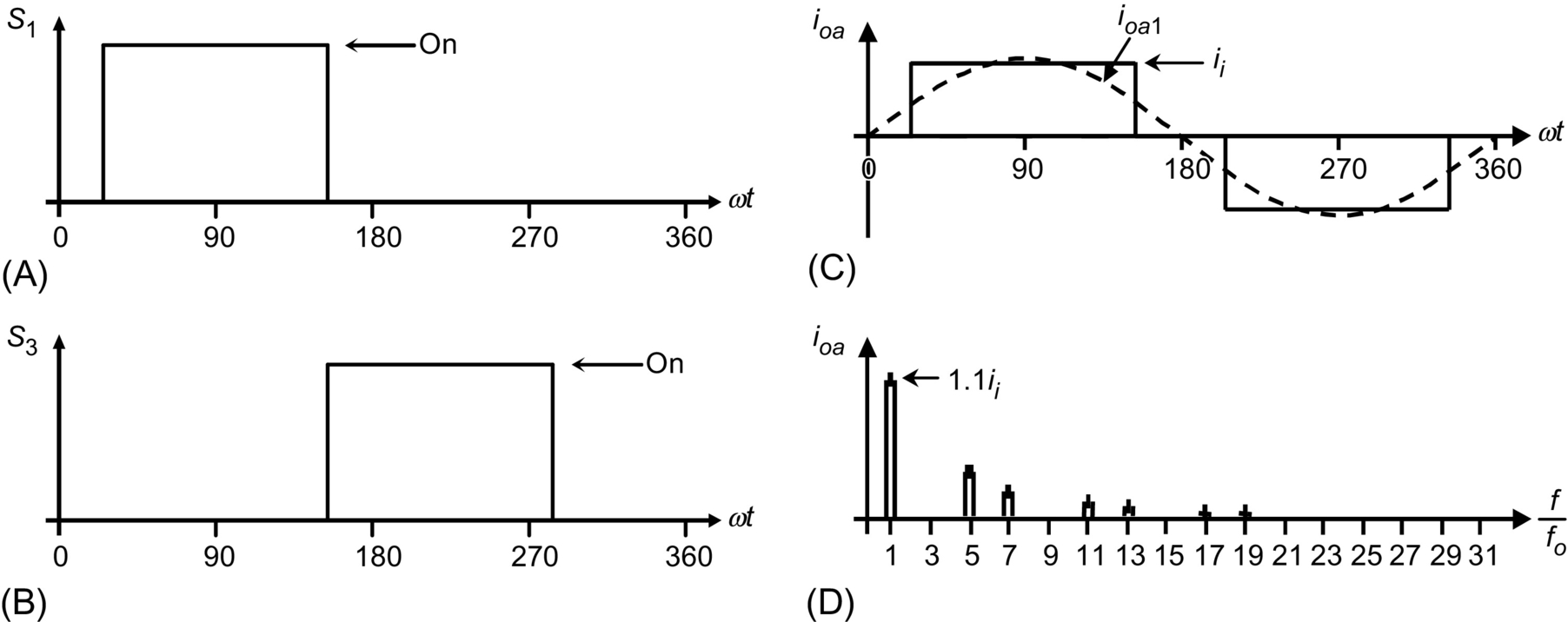
11.3.2 Square-Wave Operation of Three-phase VSIs
Large values of ma in the SPWM technique lead to full overmodulation. This is known as square-wave operation as illustrated in Fig. 11.19, where the power semiconductors are on for 180°. In this operation mode, the VSI cannot control the load voltage except by means of the dc link voltage vi. This is based on the fundamental ac line-voltage expression

ˆvab1=4π√3vi2
The ac line output voltage contains the harmonics fh, where h=6⋅k±1![]() (k=1,2,3,…
(k=1,2,3,…![]() ), and they feature amplitudes that are inversely proportional to their harmonic order (Fig. 11.18D). Their amplitudes are
), and they feature amplitudes that are inversely proportional to their harmonic order (Fig. 11.18D). Their amplitudes are
ˆvabh=1h4π√3vi2
11.3.3 Sinusoidal PWM with Zero Sequence Signal Injection
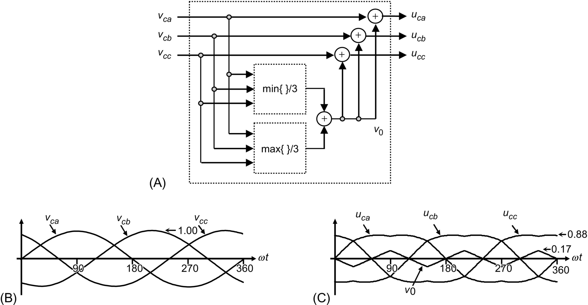
The restriction for ma (ma≤1![]() ) can be relaxed if a zero-sequence signal is added to the modulating signals before they are compared with the carrier signal. Fig. 11.20 shows the block diagram of the technique. Clearly, the addition of the zero sequence reduces the peak amplitude of the resulting modulating signals (uca, ucb, ucc)
) can be relaxed if a zero-sequence signal is added to the modulating signals before they are compared with the carrier signal. Fig. 11.20 shows the block diagram of the technique. Clearly, the addition of the zero sequence reduces the peak amplitude of the resulting modulating signals (uca, ucb, ucc)![]() , while the fundamental components remain unchanged. This approach expands the range of the linear region as it allows the use of modulation indexes ma up to 2/√3
, while the fundamental components remain unchanged. This approach expands the range of the linear region as it allows the use of modulation indexes ma up to 2/√3![]() without getting into the overmodulating region.
without getting into the overmodulating region.
 , mf=9): (A) block diagram, (B) modulating signals, and (C) zero sequence and modulating signals with zero-sequence injection.
The maximum amplitude of the fundamental phase voltage in the linear region (ma≤2/√3)![]() is vi/2; thus, the maximum amplitude of the fundamental ac output line voltage is vi. Therefore, one can write
is vi/2; thus, the maximum amplitude of the fundamental ac output line voltage is vi. Therefore, one can write
ˆvab1=ma√3vi2(0<ma≤2/√3)
Fig. 11.21 shows the ideal waveforms of a three-phase VSI SPWM with zero injection for ma=0.8![]() .
.
 , mf=9) with zero-sequence signal injection: (A) modulating signals, (B) carrier and modulating signals with zero-sequence signal injection, (C) switch S1 state, (D) ac output voltage, (E) ac output voltage spectrum, (F) ac output current, (G) dc current, (H) dc current spectrum, (I) switch S1 current, and (J) diode D1 current.
11.3.4 Selective Harmonic Elimination in Three-phase VSIs
As in single-phase VSIs, the SHE technique can be applied to three-phase VSIs. In this case, the power semiconductors of each leg of the inverter are switched so as to eliminate a given number of harmonics and to control the fundamental phase voltage amplitude. Considering that in many applications the required line output voltages should be balanced and 120° out of phase, the harmonic multiples of 3 (h=3,9,15,…![]() ), which could be present in the phase voltages (vaN, vbN, and vcN), will not be present in the load voltages (vab, vbc, and vca). Therefore, these harmonics are not required to be eliminated; thus, the chopping angles are used to eliminate only the harmonics at frequencies h=5,7,11,13,…
), which could be present in the phase voltages (vaN, vbN, and vcN), will not be present in the load voltages (vab, vbc, and vca). Therefore, these harmonics are not required to be eliminated; thus, the chopping angles are used to eliminate only the harmonics at frequencies h=5,7,11,13,…![]() as required.
as required.
The expressions to eliminate a given number of harmonics are the same as those used in single-phase inverters. For instance, to eliminate the fifth and seventh harmonics and perform fundamental magnitude control (N=3![]() ), the equations to be solved are
), the equations to be solved are
cos(1α1)−cos(1α2)+cos(1α3)=(2+πˆvaN1/vi)/4cos(5α1)−cos(5α2)+cos(5α3)=1/2cos(7α1)−cos(7α2)+cos(7α3)=1/2

where the angles α1, α2, and α3 are defined as shown in Fig. 11.22A and plotted in Fig. 11.23. Fig. 11.22B shows that the third, ninth, fifteenth, … harmonics are all present in the phase voltages; however, they are not in the line voltages (Fig. 11.22D). If necessary, higher-order harmonics not eliminated with this technique can be filtered using small filters.

11.3.5 Space-Vector (SV)-Based Modulating Techniques
At present, the control strategies are implemented in digital systems, and therefore, digital modulating techniques are also available. The SV-based modulating technique is a digital technique in which the objective is to generate PWM load line voltages that are on average equal to given load line voltages. This is done in each sampling period by properly selecting the switch states from the valid ones of the VSI (Table 11.5) and by proper calculation of the period of times they are used. The selection and calculation times are based upon the SV transformation.
11.3.5.1 Space-Vector Transformation
Any three-phase set of variables that add up to zero in the stationary abc frame can be represented in a complex plane by a complex vector that contains a real (α) and an imaginary (β) component. For instance, the vector of three-phase line-modulating signals vabcc=[vcavcbvcc]T![]() can be represented by the complex vector →vc=vαβc=[vcαvcβ]T
can be represented by the complex vector →vc=vαβc=[vcαvcβ]T![]() by means of the following transformation:
by means of the following transformation:
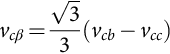
vcα=23[vca−0.5(vcb+vcc)]
vcβ=√33(vcb−vcc)
If the line-modulating signals vcabc are three balanced sinusoidal waveforms that feature an amplitude ˆvc![]() and an angular frequency ω, the resulting modulating signals in the αβ stationary frame become a vector →vc=vαβc
and an angular frequency ω, the resulting modulating signals in the αβ stationary frame become a vector →vc=vαβc![]() of fixed module ˆvc
of fixed module ˆvc![]() , which rotates at frequency ω (Fig. 11.24). Similarly, the SV transformation is applied to the line voltages of the eight states of the VSI normalized with respect to vi (Table 11.5), which generates the eight space vectors (→vi
, which rotates at frequency ω (Fig. 11.24). Similarly, the SV transformation is applied to the line voltages of the eight states of the VSI normalized with respect to vi (Table 11.5), which generates the eight space vectors (→vi![]() , i=1,2,…,8
, i=1,2,…,8![]() ) in Fig. 11.24. As expected, →v1
) in Fig. 11.24. As expected, →v1![]() to →v6
to →v6![]() are nonnull line-voltage vectors, and →v7
are nonnull line-voltage vectors, and →v7![]() and →v8
and →v8![]() are null line-voltage vectors.
are null line-voltage vectors.
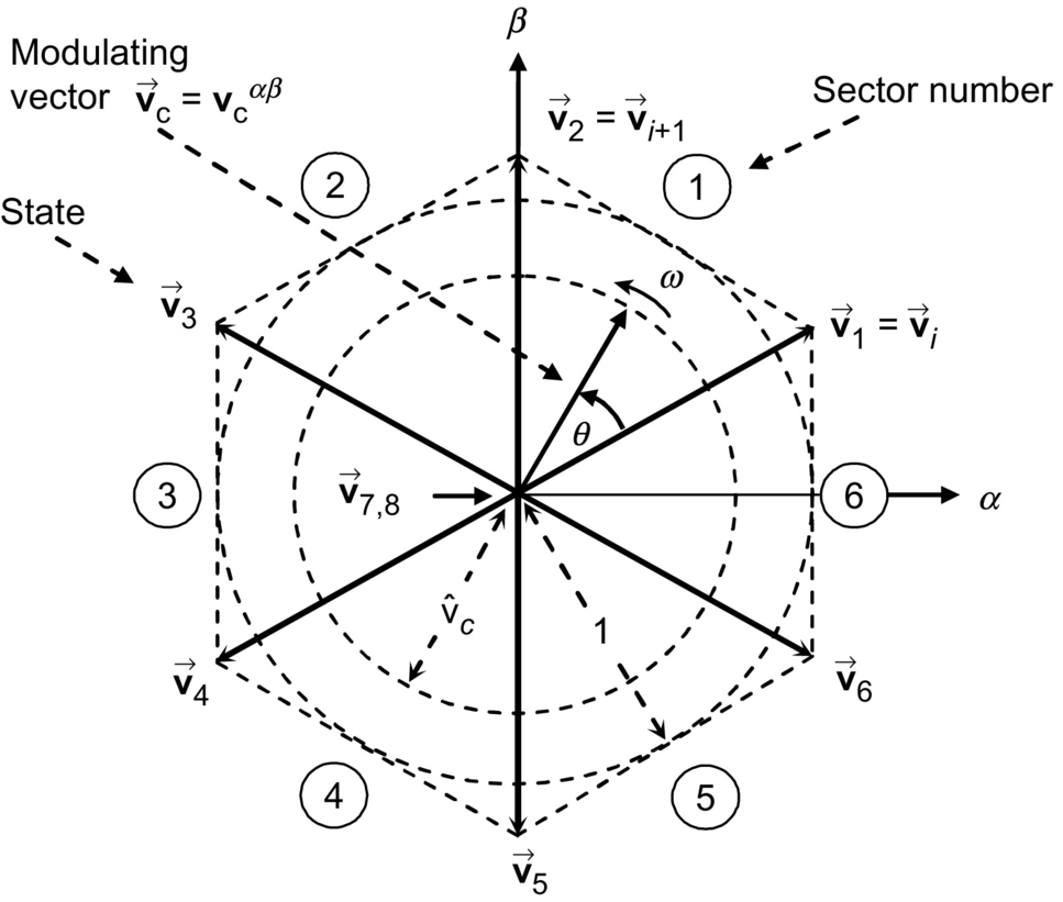
The objective of the SV technique is to approximate the line-modulating signal space vector →vc![]() with the eight space vectors (→vi
with the eight space vectors (→vi![]() , i=1,2,…,8
, i=1,2,…,8![]() ) available in VSIs. However, if the modulating signal →vc
) available in VSIs. However, if the modulating signal →vc![]() is laying between the arbitrary vectors →vi
is laying between the arbitrary vectors →vi![]() and →vi+1
and →vi+1![]() , only the nearest two nonzero vectors (→vi
, only the nearest two nonzero vectors (→vi![]() and →vi+1
and →vi+1![]() ) and the zero SV (→vz=→v7
) and the zero SV (→vz=→v7![]() or →v8
or →v8![]() ) should be used. Thus, the maximum load line voltage is maximized, and the switching frequency is minimized. To ensure that the generated voltage in one sampling period Ts (made up of the voltages provided by the vectors →vi
) should be used. Thus, the maximum load line voltage is maximized, and the switching frequency is minimized. To ensure that the generated voltage in one sampling period Ts (made up of the voltages provided by the vectors →vi![]() , →vi+1
, →vi+1![]() , and →vz
, and →vz![]() used during times Ti, Ti+1
used during times Ti, Ti+1![]() , and Tz) is on average equal to the vector →vc
, and Tz) is on average equal to the vector →vc![]() , the following expression should hold:
, the following expression should hold:
→vc⋅Ts=→vi⋅Ts+→vi+1⋅Ti+1+→vz⋅Tz
The solution of the real and imaginary parts of Eq. (11.32) for a line-load voltage that features an amplitude restricted to 0≤ˆvc≤1![]() gives
gives
Ti=Ts⋅ˆvc⋅sin(π/3−θ)
Ti+1=Ts⋅ˆvc⋅sin(θ)
Tz=Ts−Ti−Ti+1
The preceding expressions indicate that the maximum fundamental line-voltage amplitude is unity as 0≤θ≤π/3![]() . This is an advantage over the SPWM technique that achieves a √3/2
. This is an advantage over the SPWM technique that achieves a √3/2![]() maximum fundamental line-voltage amplitude in the linear operating region. Although the space-vector-modulation (SVM) technique selects the vectors to be used and their respective on-times, the sequence in which they are used, the selection of the zero space vector, and the normalized sampled frequency remain undetermined.
maximum fundamental line-voltage amplitude in the linear operating region. Although the space-vector-modulation (SVM) technique selects the vectors to be used and their respective on-times, the sequence in which they are used, the selection of the zero space vector, and the normalized sampled frequency remain undetermined.
For instance, if the modulating line-voltage vector is in sector 1 (Fig. 11.24), the vectors →v1![]() , →v2
, →v2![]() , and →vz
, and →vz![]() should be used within a sampling period by intervals given by T1, T2, and Tz, respectively. However, the sequence should be different, for example, (i) →v1−→v2−→vz
should be used within a sampling period by intervals given by T1, T2, and Tz, respectively. However, the sequence should be different, for example, (i) →v1−→v2−→vz![]() , (ii) →vz−→v1−→v2−→vz
, (ii) →vz−→v1−→v2−→vz![]() , and (iii) →vz−→v1−→v2−→v1−→vz
, and (iii) →vz−→v1−→v2−→v1−→vz![]() . Finally, the technique does not indicate whether →vz
. Finally, the technique does not indicate whether →vz![]() should be →v7
should be →v7![]() , →v8
, →v8![]() , or a combination of both.
, or a combination of both.
11.3.5.2 Space-Vector Sequences and Zero Space-Vector Selection
The sequence to be used should ensure load line voltages that feature quarter-wave symmetry in order to reduce unwanted harmonics in their spectra (even harmonics). Additionally, the zero SV selection should be done in order to reduce the switching frequency. Although there is not a systematic approach to generate a SV sequence, a graphic representation shows that the sequence →vi![]() , →vi+1
, →vi+1![]() , →vz
, →vz![]() (where vz is alternately chosen among →v7
(where vz is alternately chosen among →v7![]() and →v8
and →v8![]() ) provides high performance in terms of minimizing unwanted harmonics and reducing the switching frequency.
) provides high performance in terms of minimizing unwanted harmonics and reducing the switching frequency.
11.3.5.3 The Normalized Sampling Frequency
The normalized carrier frequency mf in three-phase carrier-based PWM techniques is chosen to be an odd integer number multiple of 3 (mf=3⋅n![]() , n=1,3,5,…
, n=1,3,5,…![]() ). Thus, it is possible to minimize parasitic or nonintrinsic harmonics in the PWM waveforms. A similar approach can be used in the SVM technique to minimize uncharacteristic harmonics. Hence, it is found that the normalized sampling frequency fsn should be an integer multiple of 6. This is due to the fact that in order to produce symmetrical line voltages, all the sectors (a total of six) should be used equally in one period. As an example, Fig. 11.25 shows the relevant waveforms of a VSI SVM for fsn=18
). Thus, it is possible to minimize parasitic or nonintrinsic harmonics in the PWM waveforms. A similar approach can be used in the SVM technique to minimize uncharacteristic harmonics. Hence, it is found that the normalized sampling frequency fsn should be an integer multiple of 6. This is due to the fact that in order to produce symmetrical line voltages, all the sectors (a total of six) should be used equally in one period. As an example, Fig. 11.25 shows the relevant waveforms of a VSI SVM for fsn=18![]() and ˆvc=0.8
and ˆvc=0.8![]() . Fig. 11.25 confirms that the first set of relevant harmonics in the load line voltage are at fsn, which is also the switching frequency.
. Fig. 11.25 confirms that the first set of relevant harmonics in the load line voltage are at fsn, which is also the switching frequency.
 , fsn=18
 ): (A) modulating signals, (B) switch S1 state, (C) switch S3 state, (D) ac output voltage, (E) ac output voltage spectrum, (F) ac output current, (G) dc current, (H) dc current spectrum, (I) switch S1 current, and (J) diode D1 current.
11.3.6 DC Link Current in Three-Phase VSIs
Due to the fact that the inverter is assumed to be lossless and constructed without storage energy components, the instantaneous power balance indicates that
vi(t)⋅ii(t)=vab(t)⋅ia(t)+vbc(t)⋅ib(t)+vca(t)⋅ic(t)
where ia(t), ib(t), and ic(t) are the phase-load currents as shown in Fig. 11.26. If the load is balanced and inductive and a relatively high switching frequency is used, the load currents become nearly sinusoidal balanced waveforms. On the other hand, if the ac output voltages are considered sinusoidal and the dc link voltage is assumed constant vi(t)=Vi![]() , Eq. (11.37) can be simplified to
, Eq. (11.37) can be simplified to

ii(t)=1Vi{√2Vo1sin(ωt)⋅√2Iosin(ωt−ϕ)+√2Vo1sin(ωt−120∘)⋅√2Iosin(ωt−120°−ϕ)+√2Vo1sin(ωt−240∘)⋅√2Iosin(ωt−240°−ϕ)}

where Vo1 is the fundamental rms ac output line voltage, Io is the rms phase-load current, and ϕ is an arbitrary inductive load power factor. Hence, the dc link current expression can be further simplified to
ii(t)=3Vo1ViIocos(ϕ)=√3Vo1ViIlcos(ϕ)
where Il=√3Io![]() is the rms load line current. The resulting dc link current expression indicates that under harmonic-free load voltages, only a clean dc current should be expected in the dc bus and, compared with single-phase VSIs, there is no presence of second harmonic. However, as the ac load line voltages contain harmonics around the normalized sampling frequency fsn, the dc link current will contain harmonics but around fsn as shown in Fig. 11.25H.
is the rms load line current. The resulting dc link current expression indicates that under harmonic-free load voltages, only a clean dc current should be expected in the dc bus and, compared with single-phase VSIs, there is no presence of second harmonic. However, as the ac load line voltages contain harmonics around the normalized sampling frequency fsn, the dc link current will contain harmonics but around fsn as shown in Fig. 11.25H.
11.3.7 Phase-Load Voltage in Three-Phase VSIs
The load is sometimes wye-connected, and the phase-load voltages van, vbn, and vcn may be required (Fig. 11.27). To obtain them, it should be considered that the line-voltage vector is
[vabvbcvca]=[van−vbnvbn−vcnvcn−van]

which can be written as a function of the phase voltage vector [vanvbnvcn]T as
[vabvbcvca]=[1−1001−1−101][vanvbnvcn]
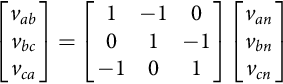
Expression (11.41) represents a linear system where the unknown quantity is the vector [vanvbnvcn]T. Unfortunately, the system is singular as the rows add up to zero (line voltages add up to zero); therefore, the phase-load voltages cannot be obtained by matrix inversion. However, if the phase-load voltages add up to zero, Eq. (11.41) can be rewritten as
[vabvbc0]=[1−1001−1111][vanvbnvcn]

which is not singular, and hence,
[vanvbnvcn]=[1−1001−1111]−1[vabvbc0]=13[211−111−1−21][vabvbc0]

that can be further simplified to
[vanvbnvcn]=13[21−11−1−2][vabvbc]
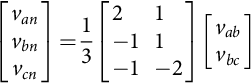
The final expression for the phase-load voltages is only a function of vab and vbc, which is due to the fact that the last row in Eq. (11.42) is chosen to be only ones. Fig. 11.28 shows the line and phase voltages obtained using Eq. (11.44).

In the particular case of a square-wave three-phase VSI, this is known as a six-step inverter because of the six voltage changes per output voltage cycle.
11.4 Three-Phase Current Source Inverters
The main objective of these static power converters is to produce an ac output current waveforms from a dc current power supply. For sinusoidal ac outputs, its magnitude, frequency, and phase should be controllable. Due to the fact that the ac line currents ioa, iob, and ioc (Fig. 11.29) feature high di/dt, a capacitive filter should be connected at the ac output. These topologies are mainly used in medium-voltage industrial applications, where high-quality voltage waveforms are required.
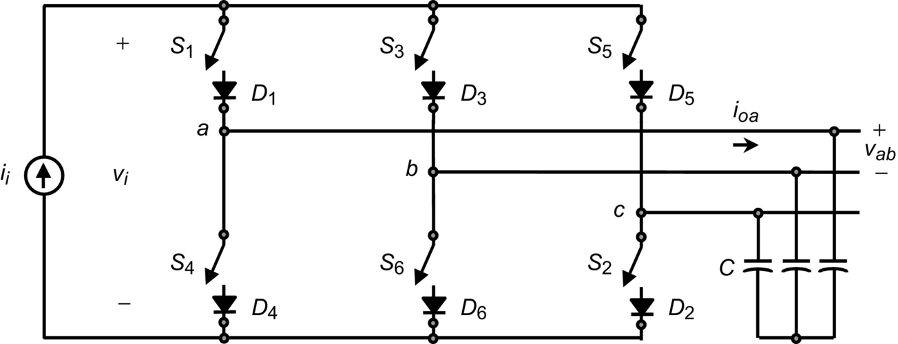
In order to properly gate the power switches of a three-phase CSI, the compulsory rules of Section 11.2.2 are valid. The main constraints are that one top switch (1, 3, or 5 (Fig. 11.29)) and one bottom switch (4, 6, or 2 (Fig. 11.29)) should be closed at any time.
There are nine valid states in three-phase CSIs. The states 7, 8, and 9 (Table 11.6) produce zero ac line currents. The remaining states (1–6 in Table 11.6) produce nonzero ac output line currents. In order to generate a given set of ac line current waveforms, the inverter must move from one state to another. Thus, the resulting line currents consist of discrete values of current, which are ii, 0, and −ii![]() . The selection of the states in order to generate the given waveforms is done by the modulating technique that should ensure the use of only the valid states.
. The selection of the states in order to generate the given waveforms is done by the modulating technique that should ensure the use of only the valid states.
Table 11.6
Valid switch states for a three-phase CSI
| State | State no. | ioa | iob | ioc |
Space vector |
| S1 and S2 are on, and S3, S4, S5, and S6 are off | 1 | ii | 0 | −ii |
→i1=1+j0.577 |
| S2 and S3 are on, and S4, S5, S6, and S1 are off | 2 | 0 | ii | −ii |
→i2=j1.155 |
| S3 and S4 are on, and S5, S6, S1, and S2 are off | 3 | −ii |
ii | 0 | →i3=−1+j0.577 |
| S4 and S5 are on, and S6, S1, S2, and S3 are off | 4 | −ii |
0 | ii | →i4=−1−j0.577 |
| S5 and S6 are on, and S1, S2, S3, and S4 are off | 5 | 0 | −ii |
ii | →i5=−j1.155 |
| S6 and S1 are on, and S2, S3, S4, and S5 are off | 6 | ii | −ii |
0 | →i6=1−j0.577 |
| S1 and S4 are on, and S2, S3, S5, and S6 are off | 7 | 0 | 0 | 0 | →i7=0 |
| S3 and S6 are on, and S1, S2, S4, and S5 are off | 8 | 0 | 0 | 0 | →i8=0 |
| S5 and S2 are on, and S6, S1, S3, and S4 are off | 9 | 0 | 0 | 0 | →i9=0 |

There are several modulating techniques that deal with the special requirements of CSIs and can be implemented. These techniques are classified into three categories: (a) the carrier-based, (b) the SHE-based, and (c) the SV-based techniques. Although they are different, they generate gating signals that satisfy the special requirements of CSIs. To simplify the analysis, a constant dc link current source is considered (ii=Ii![]() ).
).
11.4.1 Carrier-Based PWM Techniques in CSIs
It has been mentioned that the carrier-based PWM techniques that were initially developed for three-phase VSIs can be extended to three-phase CSIs. The circuit shown in Fig. 11.30 obtains the gating pattern for a CSI from the gating pattern developed for a VSI. As a result, the line current appears to be identical to the line voltage in a VSI for similar carrier and modulating signals.

It is composed of a switching pulse generator, a shorting pulse generator, a shorting pulse distributor, and a switching and shorting pulse combinator. The circuit basically produces the gating signals (s=[s1…s6]T![]() ) according to a carrier iΔ and three modulating signals iabcc=[icaicbica]T
) according to a carrier iΔ and three modulating signals iabcc=[icaicbica]T![]() .
.
The first component of this stage (Fig. 11.30) is the switching pulse generator, where the signals sa123 are generated according to
s123a={HIGH=1ifiabcc>vcLOW=0otherwise
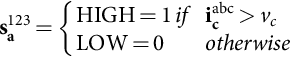
The outputs of the switching pulse generator are the signals sc, which are basically the gating signals of the CSI without the shorting pulses. These are necessary to inject the dc link current ii when no zero ac output currents are required.
In order to satisfy the first compulsory rule for CSI, the shorting pulse (sd=1![]() ) is generated by the shorting pulse generator (Fig. 11.30); this are used to produce zero ac output currents. Then, this pulse is added (using OR gates) to only one leg of the CSI (either to the switches 1 and 4, 3 and 6, or 5 and 2) by means of the switching and shorting pulse combinator (Fig. 11.30). The signals generated by the shorting pulse generator se123 not only ensure that only one leg of the CSI is shorted at any time but also give an even distribution of the shorting pulse, as se123 is high for 120° in each period. This ensures that the rms currents are equal in all legs.
) is generated by the shorting pulse generator (Fig. 11.30); this are used to produce zero ac output currents. Then, this pulse is added (using OR gates) to only one leg of the CSI (either to the switches 1 and 4, 3 and 6, or 5 and 2) by means of the switching and shorting pulse combinator (Fig. 11.30). The signals generated by the shorting pulse generator se123 not only ensure that only one leg of the CSI is shorted at any time but also give an even distribution of the shorting pulse, as se123 is high for 120° in each period. This ensures that the rms currents are equal in all legs.
Fig. 11.31 shows the relevant waveforms if a triangular carrier iΔ and sinusoidal modulating signals icabc are used in combination with the gating pattern generator circuit (Fig. 11.30); this is SPWM in CSIs. It can be observed that some of the waveforms (Fig. 11.31) are identical to those obtained in three-phase VSIs, where an SPWM technique is used (Fig. 11.18). Specifically, (i) the load line voltage (Fig. 11.18D) in the VSI is identical to the load line current (Fig. 11.31D) in the CSI and (ii) the dc link current (Fig. 11.18G) in the VSI is identical to the dc link voltage (Fig. 11.31G) in the CSI.
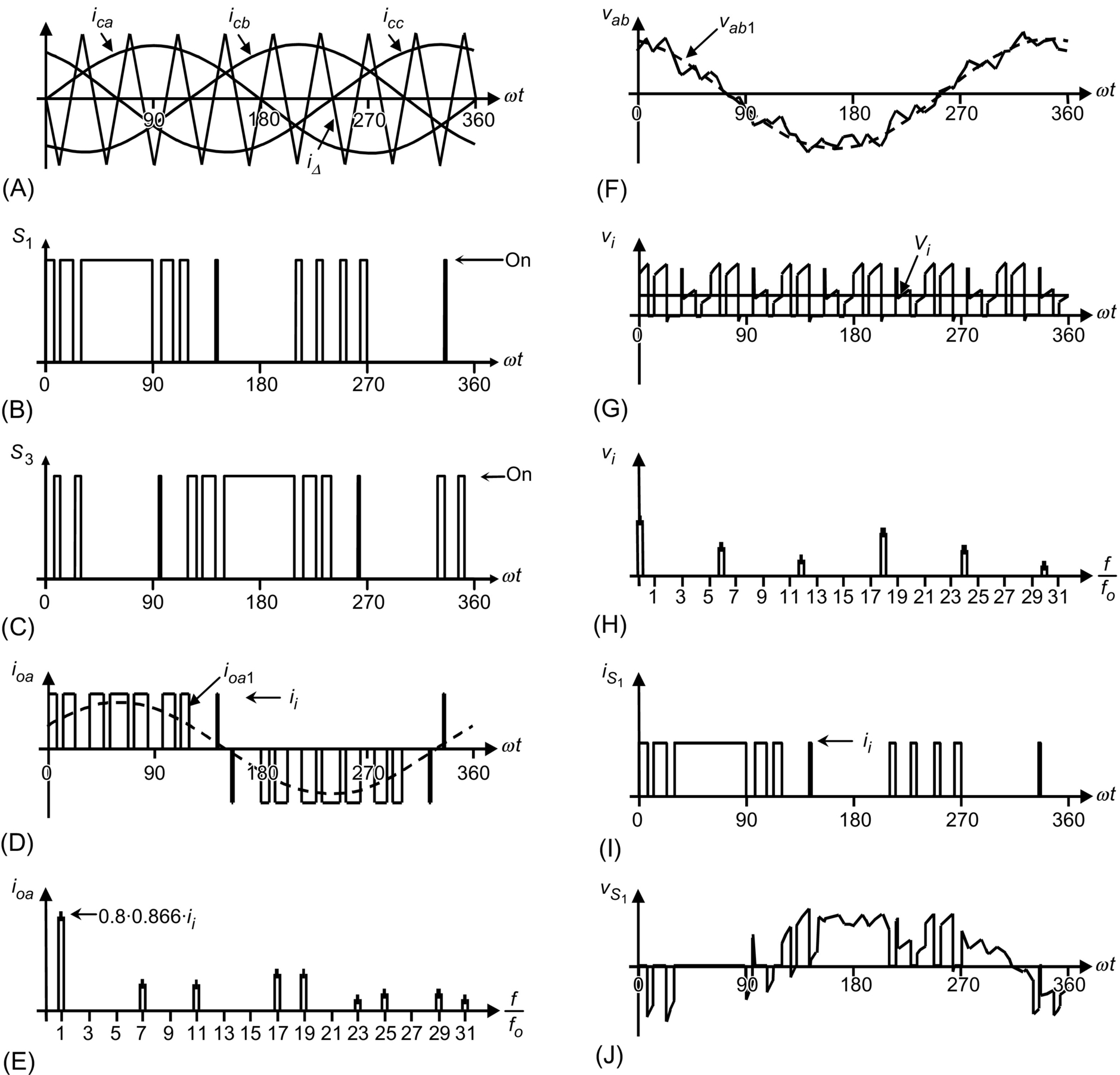 , mf=9): (A) carrier and modulating signals, (B) switch S1 state, (C) switch S3 state, (D) ac output current, (E) ac output current spectrum, (F) ac output voltage, (G) dc voltage, (H) dc voltage spectrum, (I) switch S1 current, and (J) switch S1 voltage.
This brings up the duality issue between both the topologies when similar modulation approaches are used. Therefore, for odd multiples of 3 values of the normalized carrier frequency mf, the harmonics in the ac output current appear at normalized frequencies fh centered around mf and its multiples, specifically, at
h=lmf±kl=1,2,…
where l=1,3,5,…![]() for k=2,4,6,…
for k=2,4,6,…![]() and l=2,4,…
and l=2,4,…![]() for k=1,5,7,…
for k=1,5,7,…![]() such that h is not a multiple of 3. Therefore, the harmonics will be at mf±2
such that h is not a multiple of 3. Therefore, the harmonics will be at mf±2![]() , mf±4,…
, mf±4,…![]() , 2mf±1
, 2mf±1![]() , 2mf±5,…
, 2mf±5,…![]() , 3mf±2
, 3mf±2![]() , 3mf±4,…
, 3mf±4,…![]() , 4mf±1
, 4mf±1![]() , 4mf±5,…
, 4mf±5,…![]() . For nearly sinusoidal ac load voltages, the harmonics in the dc link voltage are at frequencies given by
. For nearly sinusoidal ac load voltages, the harmonics in the dc link voltage are at frequencies given by
h=lmf±k±1l=1,2,…
where l=0,2,4,…![]() for k=1,5,7,…
for k=1,5,7,…![]() and l=1,3,5,…
and l=1,3,5,…![]() for k=2,4,6,…
for k=2,4,6,…![]() such that h=l⋅mf±k
such that h=l⋅mf±k![]() is positive and not a multiple of 3. For instance, Fig. 11.31H shows the sixth harmonic (h=6
is positive and not a multiple of 3. For instance, Fig. 11.31H shows the sixth harmonic (h=6![]() ), which is due to h=1⋅9−2−1=6
), which is due to h=1⋅9−2−1=6![]() . Identical conclusions can be drawn for the small and large values of mf in the same way as for three-phase VSI configurations. Thus, the maximum amplitude of the fundamental ac output line current is ˆioa1=√3ii/2
. Identical conclusions can be drawn for the small and large values of mf in the same way as for three-phase VSI configurations. Thus, the maximum amplitude of the fundamental ac output line current is ˆioa1=√3ii/2![]() , and therefore, one can write
, and therefore, one can write
ˆioa1=ma√32ii0<ma≤1

To further increase the amplitude of the load current, the overmodulation approach can be used. In this region, the fundamental line currents range in
√32ii<ˆioa1=ˆiob1=ˆioc1<4π√32ii

To further test the gating signal generator circuit (Fig. 11.30), a sinusoidal set with third- and ninth-harmonic injection modulating signals are used. Fig. 11.32 shows the relevant waveforms.
 , mf=15
 ): signals as described in Fig. 11.30.
11.4.2 Square-Wave Operation of Three-phase CSIs
As in VSIs, large values of ma in the SPWM technique lead to full overmodulation. This is known as square-wave operation. Fig. 11.33 depicts this operating mode in a three-phase CSI, where the power semiconductors are on for 120°. As presumed, the CSI cannot control the load current except by means of the dc link current ii. This is due to the fact that the fundamental ac line current expression is
ˆioa1=4π√32ii
The ac line current contains the harmonics fh, where h=6⋅k±1![]() (k=1,2,3,…
(k=1,2,3,…![]() ), and they feature amplitudes that are inversely proportional to their harmonic order (Fig. 11.33D). Thus,
), and they feature amplitudes that are inversely proportional to their harmonic order (Fig. 11.33D). Thus,
ˆioah=1h4π√32ii
The duality issue among both the three-phase VSI and CSI should be noted especially in terms of the line-load waveforms. The line-load voltage produced by a VSI is identical to the load line current produced by the CSI when both are modulated using identical techniques. The next section will show that this also holds for SHE-based techniques.
11.4.3 Selective Harmonic Elimination in Three-phase CSIs
The SHE-based modulating techniques in VSIs define the gating signals such that a given number of harmonics are eliminated and the fundamental phase voltage amplitude is controlled. If the required line output voltages are balanced and 120° out of phase, the chopping angles are used to eliminate only the harmonics at frequencies h=5,7,11,13,…![]() as required.
as required.
The circuit shown in Fig. 11.34 uses the gating signals sa123 developed for a VSI and a set of synchronizing signals icabc to obtain the gating signals s for a CSI. The synchronizing signals icabc are sinusoidal balanced waveforms that are synchronized with the signals sa123 in order to symmetrically distribute the shorting pulse and thus generate symmetrical gating patterns. The circuit ensures line current waveforms as the line-voltage ones in a VSI. Therefore, any arbitrary number of harmonics can be eliminated, and the fundamental line current can be controlled in CSIs. Moreover, the same chopping angles obtained for VSIs can be used in CSIs.

For instance, to eliminate the fifth and seventh harmonics, the chopping angles are shown in Fig. 11.35, which are identical to that obtained for a VSI using Eq. (11.10). Fig. 11.36 shows that the line current does not contain the fifth and the seventh harmonics as expected. Hence, any number of harmonics can be eliminated in three-phase CSIs by means of the circuit (Fig. 11.34) without the hassle of how to satisfy the gating signal constrains.