
Power Electronic Modules
Enrico Santi University of South Carolina, Columbia, SC, United States
Soheila Eskandari University of South Carolina, Columbia, SC, United States
Bo Tian University of South Carolina, Columbia, SC, United States
Kang Peng Infineon Technologies AG Design Center, Tewksbury, MA, United States
Abstract
A power electronic module or power module is an assembly containing several power components, mostly power semiconductor devices, properly internally interconnected to perform a power conversion function. It is an integrated building block for the realization of a power converter with a reduced number of external components required. Control electronics such as gate drivers, sensing, and protection functions may be included inside the power module package. In this case, the term intelligent power module is commonly used. From the electric standpoint, the power module reduces parasitic elements in the interconnection of the power semiconductor devices due to the tight physical integration. From the thermal standpoint, the power module usually has a thermally conductive baseplate that can be bolted to a heat sink or a cold plate to remove the loss heat generated as a result of power converter operation. From the mechanical standpoint, it provides a robust mechanical package for the power components inside. In conclusion, a power module is an electro-thermo-mechanical device optimized for power converter operation. Using a power module may simplify the design of a power converter because the power module design provides a robust mechanical structure and guarantees proper operation from an electric and thermal point of view as long as the module datasheet specifications and guidelines are followed. Power modules are typically used at higher power levels, where a discrete component implementation would require paralleling of several power semiconductor devices.
Keywords
Power module; Intelligent power module; Gate drivers; Sensing; IGBT; MOSFET; Diode; Kelvin contact; Power management
6.1 Introduction
A power electronic module or power module is an assembly containing several power components, mostly power semiconductor devices, properly internally interconnected to perform a power conversion function. It is an integrated building block for the realization of a power converter with a reduced number of external components required. Control electronics such as gate drivers, sensing, and protection functions may be included inside the power module package. In this case, the term intelligent power module (IPM) is commonly used. From the electric standpoint, the power module reduces parasitic elements in the interconnection of the power semiconductor devices due to the tight physical integration. From the thermal standpoint, the power module usually has a thermally conductive baseplate that can be bolted to a heat sink or a cold plate to remove the loss heat generated as a result of power converter operation. From the mechanical standpoint, it provides a robust mechanical package for the power components inside. In conclusion, a power module is an electro-thermo-mechanical device optimized for power converter operation. Using a power module may simplify the design of a power converter because the power module design provides a robust mechanical structure and guarantees proper operation from an electric and thermal point of view as long as the module datasheet specifications and guidelines are followed. Power modules are typically used at higher power levels, where a discrete component implementation would require paralleling of several power semiconductor devices.
Advantages of power modules are tight integration of multiple power semiconductor devices, high current and power ratings because multiple power semiconductor dies can be paralleled inside the module, good thermal management, and mechanical robustness. Probably, the biggest advantage is the reduction of parasitic elements, in particular parasitic inductances, due to the tight integration. These parasitic elements cause additional losses and overshoot and ringing during converter operation, which cause electromagnetic interference (EMI) issues. The parasitic element reduction allows switching converter operation at higher frequency, which reduces passive filtering element size, and may provide additional system-level advantages, such as quiet converter operation at switching frequencies above the audible range.
The main disadvantage of power modules is probably a higher cost compared with discrete devices. A second disadvantage is that a specific application may require characteristics not available in commercial modules on the market.
In this article, power electronic modules will be described mostly from the point of view of a power module user, somebody who wants to use a power module to realize a power converter rather than the point of view of the designer of a power module.
In Section 6.2, the differences between discrete devices and modules are discussed. Section 6.3 gives an example of a power module. Section 6.4 briefly describes the manufacturing process of power modules. Section 6.5 describes various types of modules and the types of power semiconductor devices used in them. Section 6.6 discusses thermal management and Section 6.7 module reliability. Finally, Section 6.8 provides design guidelines and considerations for the use of power modules.
6.2 Discrete Power Devices Versus Power Modules
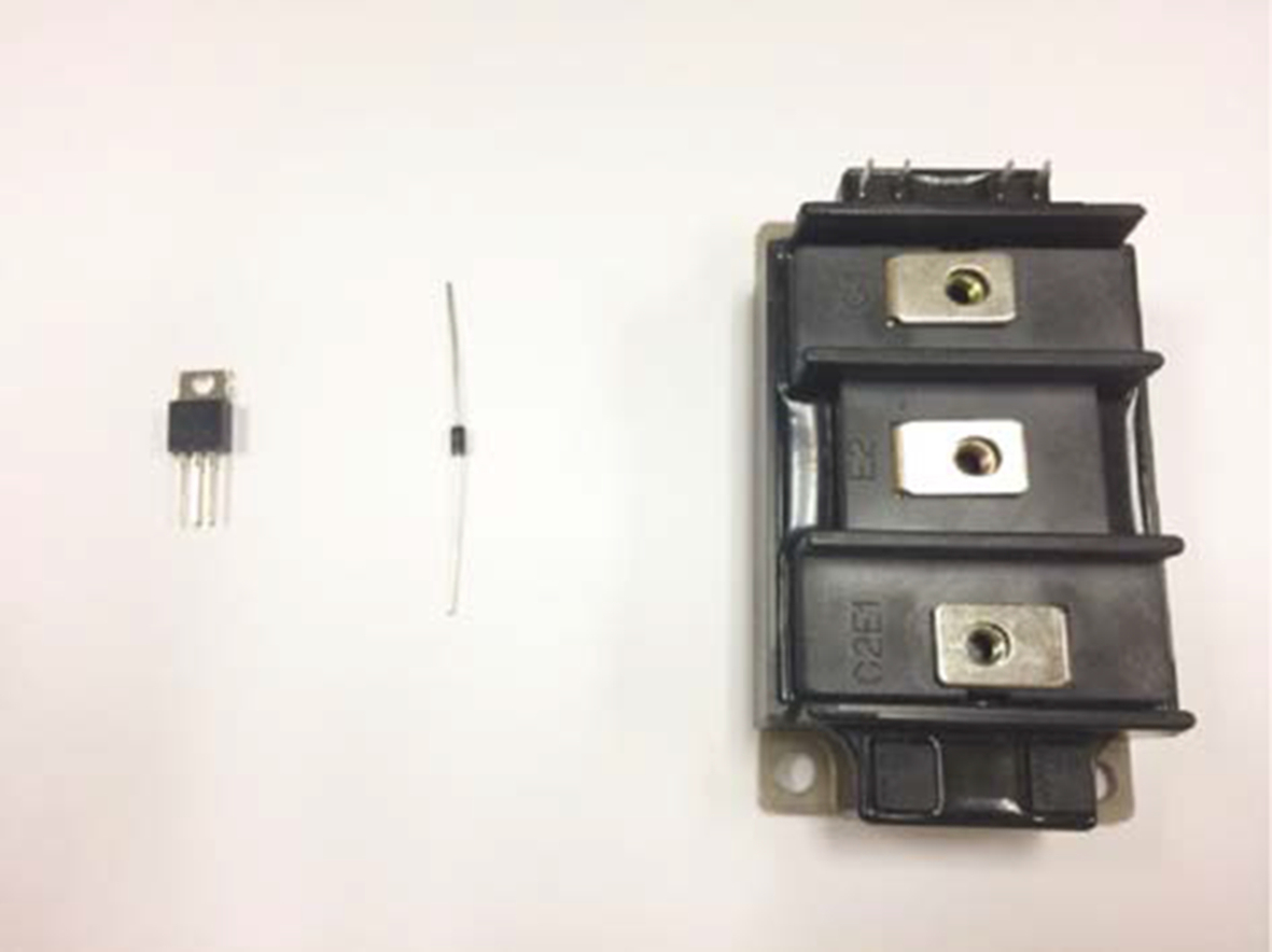
Fig. 6.1 shows a photo of two discrete semiconductor components—a power metal-oxide-semiconductor field-effect transistor (MOSFET) and a diode—and a power module. The power module is a half-bridge configuration realized with silicon insulated-gate bipolar transistors (IGBTs). The module ratings are from 1200 V to 100 A. Notice that the power module has multiple power and control connections. The module of Fig. 6.1 has three large screw-type power connections for the power terminals and four smaller pin-type connections on top for the IGBT gate terminals. The bottom of the module has a metal baseplate that can be bolted to a heat sink for thermal management. Two of the baseplate holes for heat sink mount can be clearly seen at the bottom. Notice that a discrete component contains a single power semiconductor device in an individual package, whereas the power module contains multiple power semiconductor devices. A second difference is that for discrete devices, the metal plate for heat sink connection, if provided like in the discrete MOSFET of Fig. 6.1, is typically nonisolated, whereas in the power module, all semiconductor devices are thermally coupled to the baseplate but are electrically isolated from it. In the TO220 discrete MOSFET, the metal tab is electrically connected to the drain of the MOSFET, and electric isolation must be provided as part of the heat sink mount.
6.3 An Example of Power Module
In this section, an example of an IGBT half-bridge power module is described. The physical structure of the power module with labeled terminal connections is shown in Fig. 6.2.
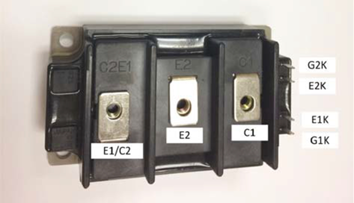
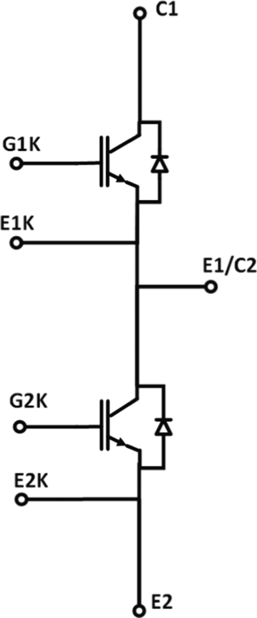
The equivalent circuit of the module is shown in Fig. 6.3 with labeled terminals. The top IGBT, called IGBT1, has collector terminal C1 and emitter terminal E1. The gate and emitter Kelvin terminals are called G1K and E1K, respectively (Kelvin contacts are discussed in Section 6.8.3). Labeling is similar for IGBT2, the bottom IGBT. Note that the module contains four distinct semiconductor devices, two IGBTs and two diodes. Each of these may consist of a single die or multiple dies connected in parallel to achieve higher current capability.
The IGBT half-bridge power module can be used to realize different switching power converters such as a bidirectional DC-DC converter (buck type in one direction and boost type in the other direction) or a single-phase two-level inverter. Three modules could be combined to create a three-phase inverter, but in that case, using a single three-phase module may be more convenient. Some of the external components required to realize a switching power converter are shown in Fig. 6.4. First of all, gate drivers are required to control the IGBTs. In a switching converter, the two IGBTs are turned on in a complementary fashion, so that, when one IGBT is on, the other one is off. The gate driver controls should introduce a short dead time during which both switches are off to prevent shoot-through, that is, shorting capacitor CBYPASS. Second, a bypass capacitor CBYPASS is required to filter the square-wave current at the switching frequency drawn by the power module during operation. As will be described later, capacitor CBYPASS should be a high-frequency capacitor and should be placed physically close to the module to minimize interconnection parasitic inductance, which causes overshoot and ringing during switching operation. Finally, an inductor L is required to filter the square-wave voltage at the switching frequency created at node E1/C2 by the switching action. Sources and loads can then be connected to the 1-2 and 3-2 ports.

6.4 Manufacturing Process
As mentioned above, power modules contain multiple power devices internally interconnected to realize a specific power processing function, such as the IGBT half-bridge module package shown in Fig. 6.2. As shown in the equivalent circuit of Fig. 6.3, this module contains multiple IGBT and diode chips interconnected to form a half-bridge topology. Physically, a power module is an integration of semiconductor chips, wire bonds, direct bonded copper (DBC) substrate, solder, baseplate, silicone gel, terminals, housing, and so on as shown in Fig. 6.5. The manufacturing process includes attaching chips on the DBC substrate, bonding wires, attaching the DBC substrate to the baseplate, placing the top housing, and filling it with silicone gel. Each element of the generic power module of Fig. 6.5 has a specific function, and its selection depends on many factors. The semiconductor chips are selected to provide the required voltage and current ratings. The DBC substrate provides electric isolation but good thermal coupling between the chips and the baseplate, so that heat generated on the chips can be efficiently conducted to the baseplate. The top copper layer provides the required electric connections among the bottom terminals of the chips. Wire bonds provide the required electric connections for the top terminals of the chips and connections to the module terminals. The baseplate provides mechanical support for the module and can be connected to a heat sink for heat removal. These elements and the techniques used for power module assembly will be described more in detail in the following subsections.

6.4.1 Semiconductor Chips
The semiconductor chips form the core of a power electronic module. Fig. 6.6 shows the interior of a power electronic module with semiconductor chips mounted on a DBC substrate and interconnected with wire bonds. Semiconductor chips determine the voltage, current, and power ratings of the power module. Power modules with different internal interconnections of semiconductor chips are available to realize different power converter topologies such as half bridge and full bridge. To achieve high-current capability, multiple semiconductor chips can be paralleled inside the module. The performance of power modules in terms of on-resistance, switching speed, and power loss is critically dependent on the semiconductor chip characteristics.
6.4.2 Die Attach
Die attach is the process of attaching a die/chip to a substrate or package. For example, in the power module of Fig. 6.5, the IGBT chip and the diode chip are attached to the top copper layer of the DBC substrate. Note that in case of vertical chip devices, the device power terminals are on opposite sides of the chip, and therefore, the chip current flows through the die attach joint. Die attach is usually accomplished by using one of the following processes: (1) eutectic, (2) solder, (3) adhesive, (4) glass or silver glass:
1) A eutectic bond is formed by melting a preform consisting of a mixture or alloy of two or more dissimilar metals in the joint between the die and substrate. The preform has a melting point that is lower than the melting point of its base materials. For example, considering a typical preform composed of gold and silicon, the melting point of gold is 1640°C, and the melting point of silicon is 1414°C. However, when the materials are combined in a preform, the melting point drops to 363°C [1].
2) Solder is an attaching method commonly used in the semiconductor industry. Solder attach provides good mechanical strength, high thermal conductivity, and good electric conductivity. Lead-based solder has been popular for a long time with advantages of good performance, proved technology, and low cost. However, environmental concerns about the toxic properties of lead have recently arisen. As a result, lead-free solder is gradually replacing lead-based solder in many applications.
3) An adhesive bond is formed by attaching the die to the substrate using some type of adhesive material. It can be electrically insulating or conductive depending on the adhesive material used. An advantage of adhesive bonding is that it is performed at room temperature and does not require high temperatures.
4) A glass bond is formed by attaching the die to the substrate using glass in paste form. The glass paste may also contain silver particles that enhance thermal and electric conductivity (this is called silver-glass die bonding). The glass bonding process is similar to adhesive bonding. The differences are the material used and the need for heat. Glass bonds are heated to 350–450°C that melts the glass into a low viscosity liquid. The glass hardens as it cools, thereby making the bond [1].
6.4.3 Wire Bonds
The electric connections between the top connections of semiconductor chips and module terminals are realized by wire bonding (shown in Figs. 6.5 and 6.6). Conventional wire bonding materials include aluminum (Al), copper (Cu), and gold (Au). Aluminum is the most common material for power modules because of its low cost and convenient process, especially to form thick wires for high-current capability. Gold has the lowest resistivity and good high-frequency performance and is usually used for integrated circuit and high-frequency devices. Due to limited improvement of resistance in power module and high cost, gold is not commonly used in power modules. The electric properties of copper are intermediate between those of Al and Au, whereas the cost of aluminum is significantly lower than copper. Consequently, Al wire bonds are most common with copper used in special cases.
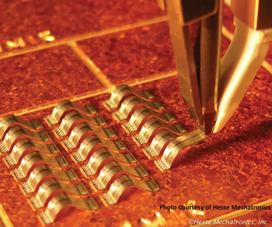
To satisfy high-current requirements, heavy wire bonding (Fig. 6.7) has been developed. Traditional wire size is smaller than 10 mils (1 mil=1/1000 in.) in diameter, whereas heavy wire bonding is significantly thicker and can save space on the bonding pad. An alternative solution is ribbon bonding (Fig. 6.8), which has the added advantage of better high-frequency performance [2]. Ribbon bonding is a form of wedge bonding using flat ribbon to replace the round wire. Compared with round wire, ribbon wire can carry higher current at high frequency, where skin effect is the limiting factor, and has smaller effective inductance and less signal cross talk [3].

6.4.4 DBC Substrate
The DBC substrate is an important interface between the electric components in the power module and the external cooling system [4]. It consists of a ceramic insulator layer with copper bonded to one or both sides by a high-temperature melting and diffusion process. DBC substrates provide electric conduction on the top copper layer, electric isolation from top to bottom thanks to the ceramic insulator layer, and outstanding thermal conduction from top to bottom. The top copper layer is etched to form the required electric interconnections and is electrically connected to the backside electrodes of semiconductor chips using one of the die attach techniques described above, most commonly by soldering. The excellent electric isolation is provided by the ceramic material. The two most common choices are alumina (Al2O3) and aluminum nitride (AlN). Al2O3 is inexpensive and widely used; however, it has the disadvantages of having relatively low thermal conductivity (24–28 W/m K) and of being brittle. Compared with Al2O3, AlN is more expensive, but it has better mechanical and thermal performance (thermal conductivity larger than 150 W/m K) and therefore has become popular in high-temperature applications [5]. The bottom copper layer is usually not patterned and is soldered to the baseplate to achieve heat spreading from top to bottom. One important thermal characteristic of DBC substrates is a low coefficient of thermal expansion (CTE), which is close to that of silicon. This ensures good thermal cycling performance and higher reliability.
6.4.5 Baseplate
One of the main functions of the baseplate is to provide mechanical support for the electric components and the DBC substrate. At the same time, it must propagate the heat generated by the semiconductor chips to the external heat sink effectively. A high degree of surface smoothness is also required to guarantee no voids between the baseplate and the DBC substrate, because voids can cause hot spots that will eventually lead to cracking and poor reliability [4]. In order to reduce the thermal resistance of the interface between the baseplate and the heatsink, a thin layer of thermal grease (also called thermal paste or heatsink compound) is applied between the baseplate and the heat sink. The purpose of the thermal grease is to fill up voids due to interface surface imperfections, because air in these voids acts as an excellent thermal insulator. However, thermal grease is not a good thermal conductor, so a thick layer of thermal grease may actually increase the thermal resistance between the baseplate and the heat sink.
CTE mismatch is a key consideration in power module design and needs to be addressed in each connection and attachment between two different materials inside the power module. To improve power module mechanical reliability, adjacent materials should have closely matched CTEs, so that, when the module heats up and cools down during operation, the adjacent materials expand and contract in a similar way, avoiding the development of mechanical stress, which can cause joint failure due to mechanical fatigue. This is particularly important for large-area connections, which may develop larger mechanical stress during thermal cycling. Therefore, the baseplate material should be thermally compatible with the DBC substrate material, and mechanical, chemical, and other factors also need to be considered.
The housing and silicone gel are used to insulate the electric components on the top of the module and prevent contamination. In modern IPMs, thermal sensors are attached to the DBC close to the chips, to measure the real-time junction temperature, which is very useful for device condition monitoring.
6.5 Types of Power Electronic Modules
There are several different types of power electronic modules available on the market today. They come in different shapes and sizes and can be categorized either by the power processing topology used or by the power semiconductor devices used.
6.5.1 A Survey of Power Electronic Module Topologies
A brief survey of power electronic module topologies is now given:
Diode rectifier or thyristor rectifier: Four (or more) diodes or thyristors are connected in a bridge circuit configuration that converts an AC input (typically either single phase or three phase) into a DC output. A full-bridge and a three-phase bridge diode rectifier are shown in Fig. 6.9. For an example of a three-phase module, see Ref. [6].
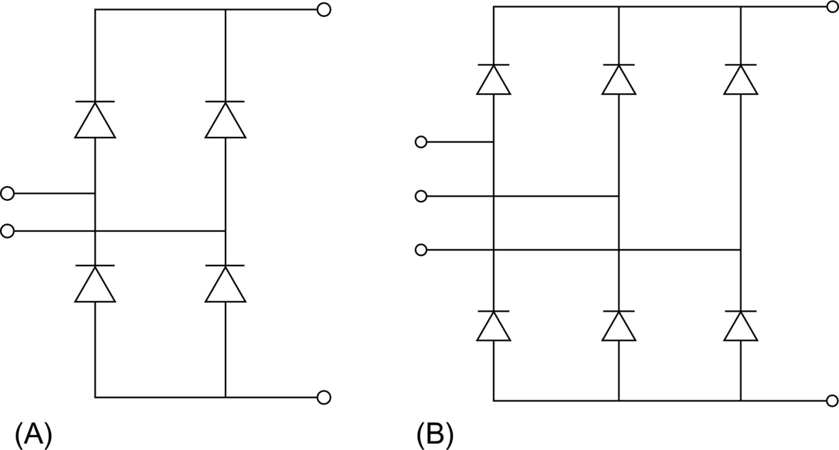
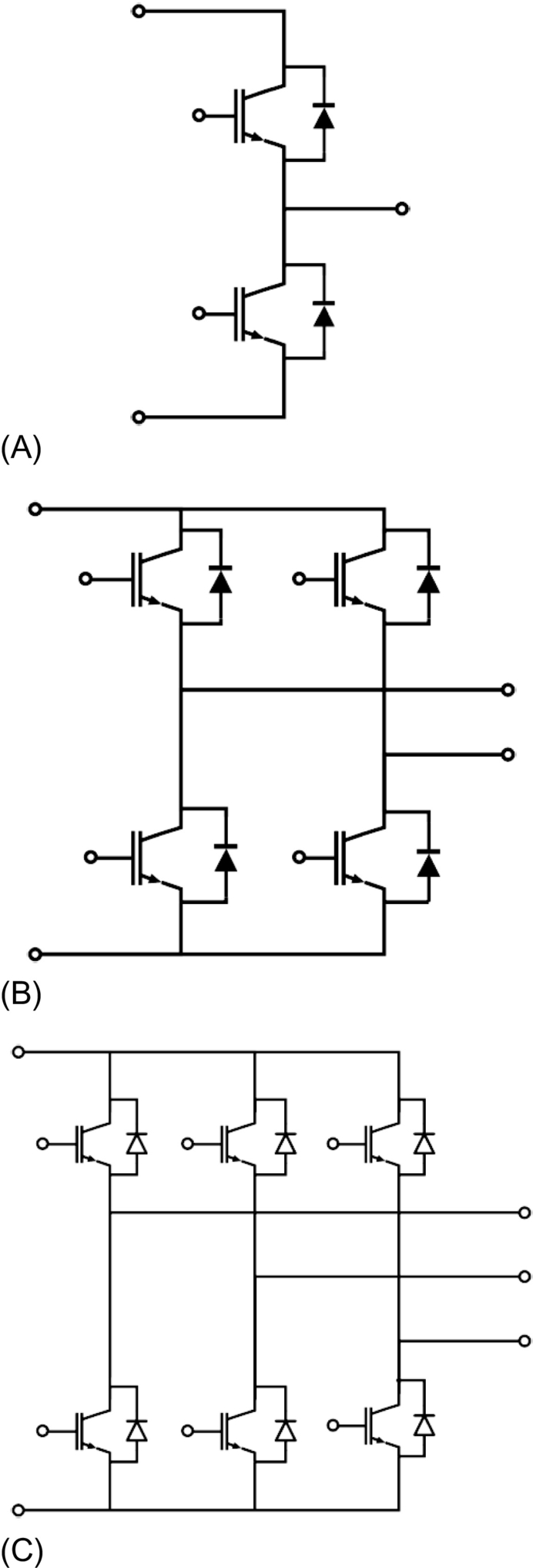
• Half-bridge, full-bridge, or three-phase (six-pack) power module: Generally, these power modules, shown in Fig. 6.10, are implemented with either power MOSFETs or IGBTs (insulated-gate bipolar transistors). Typically, IGBTs can achieve much higher current and voltage ratings, allowing them to operate at higher power levels with reduced conduction losses, whereas MOSFETs can operate at much higher switching frequencies, making them suitable for application where fast switching and high power density are required. A half-bridge configuration can be used to implement a DC-DC power-bidirectional converter or a single-phase inverter. A full-bridge configuration can be used to implement a full-bridge converter or a three-level single-phase inverter. A six-pack power module can be used to implement a three-phase inverter or a three-phase-controlled rectifier. Note that since all switches are controllable, all these converter topologies are power bidirectional, that is, power can flow in both directions. For an example of a six-pack power module, see Ref. [7].
• Converter-inverter-brake (CIB) module: The module, shown in Fig. 6.11, contains a single-phase or three-phase uncontrolled or half-controlled bridge rectifier (C) plus an inverter (I) and a brake chopper (B). This module contains all power semiconductor devices required to implement a three-phase variable motor drive fed by three-phase power. The three-phase diode rectifier can be used to create a DC bus voltage that supplies the three-phase inverter connected to the three-phase motor. The chopper circuit allows to pulse-width modulate a braking resistor to dissipate energy during regenerative braking. See Ref. [8] for more information about regeneration in motor drives.

• Neutral-point-clamped (NPC) module: Each leg has four power switches connected in series. The applied voltage on the power switch is one-half that of a two-level converter. The NPC topology can allow operation at voltages larger than the voltage rating of a single power device. In addition, NPC converter can achieve lower output current ripples and improve the total harmonic distortion (THD) of the output.
• Power factor correction (PFC) module: PFC module combines a rectifying function and a PFC function in order to reduce the harmonics of the input current and improve power factor.
6.5.2 Power Semiconductor Devices Used in Power Electronic Modules
The most common power semiconductor devices used in power electronic modules are diodes, MOSFETs, IGBTs, and thyristors. Power bipolar junction transistors (BJTs) are less common and are briefly mentioned for completeness.
1. Power diode:
Power diodes provide uncontrolled rectification of power and are used in applications such as AC-DC converters and variable-frequency drives. Typically, the power diode can be either a P-i-N diode or a Schottky diode.
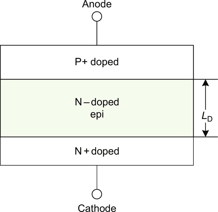
The P-i-N diode is a bipolar device having a so-called P-i-N structure, that is, it is a p-n junction with a wide, undoped intrinsic semiconductor layer (i-layer) in the middle to sustain a reverse blocking voltage. Frequently, the midlayer, rather than being intrinsic, has low N-doping and is therefore called N- (N minus) layer. Fig. 6.12 shows the basic structure of a P-i-N diode. In the forward-biased conduction, the diode has a forward conduction drop, which causes conduction loss, and the diode can be modeled as a junction voltage source, equal to the threshold voltage, and a series equivalent resistance that represents the increasing slope in the diode I-V characteristics. In the reverse-biased condition, a small reverse leakage current flows, which increases gradually with the applied reverse voltage. If the applied reverse voltage exceeds a certain voltage, called breakdown voltage, the reverse current becomes very large due to avalanche breakdown, and the diode may be destroyed due to large power dissipation in the device. The advantage of a P-i-N diode is low on-state voltage drop in high-current conduction, due to the minority carrier injection in epitaxial drift region resulting in conductivity modulation. However, the minority carrier injection during conduction causes a large reverse recovery current during diode turnoff, which is not desirable, because it causes additional turn-on loss in the active switch.
The Schottky diode is a very attractive unipolar device, formed by an electrically nonlinear contact between a metal and a semiconductor bulk region shown in Fig. 6.13. It has low on-state voltage drop, almost zero reverse recovery charge, and extremely high switching speed, but its reverse leakage current is large especially at high temperature due to its lower built-in potential barrier. Additionally, the breakdown voltage of Schottky diode is limited by the increase of drift region resistance without any conductivity modulation effect.

2. Power MOSFET
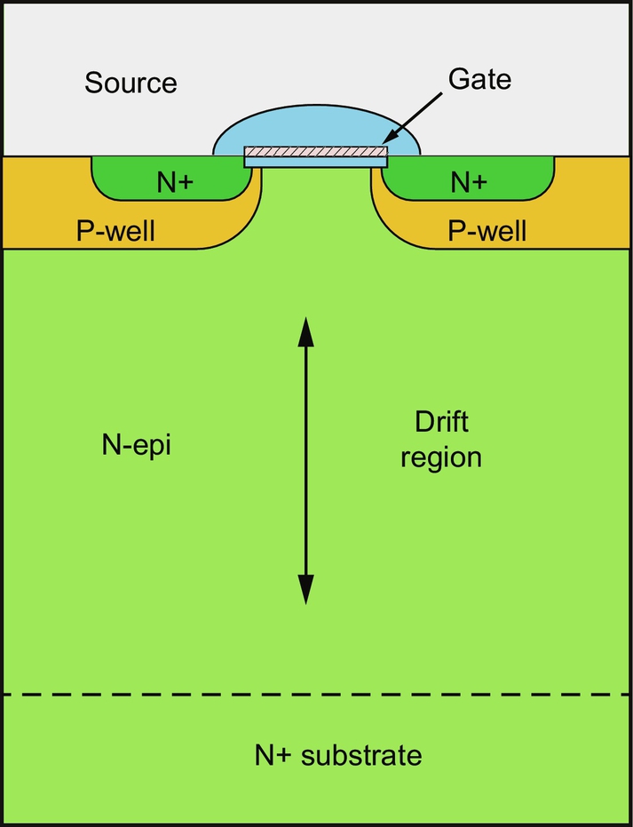
The power metal-oxide-semiconductor field-effect transistor (MOSFET) is a unipolar, majority carrier, and voltage-controlled device. It is one of the most commonly used power devices due to its easy gate driving, fast switching speed, and low loss dissipation. Most power MOSFETs feature a vertical structure (a structure of alternating p-type and n-type doping) shown in Fig. 6.14. In most power MOSFETs, the N+ source and P-well junction are shorted to prevent the parasitic bipolar transistor from turning on accidentally. When no gate voltage is applied, the power MOSFET is capable of supporting a drain-source blocking voltage through the reverse-biased P-well and N-epi junction. In high-voltage devices, most of the blocking voltage is supported by the lightly doped N-epi layer.
Generally speaking, the power MOSFET can operate in two different quadrants of its I-V characteristics: the first quadrant operation and the third quadrant operation. As the gate voltage (VG) increases above a threshold voltage (Vth), the MOSFET starts to conduct current. When the gate voltage VG is much larger than the threshold voltage Vth, the output I-V curve appears linear, and the MOSFET channel is fully turned on. Under low gate overdrive, the drain current reaches a saturation value when the MOSFET channel is pinched off.
The MOSFET's switching behavior is highly dependent on the parasitic capacitances gate-to-source Cgs, gate-to-drain Cgd, and drain-to-source Cds. Gate-to-drain capacitance Cgd and drain-to-source Cds are nonlinear and a function of bias voltages.
3. Power IGBT
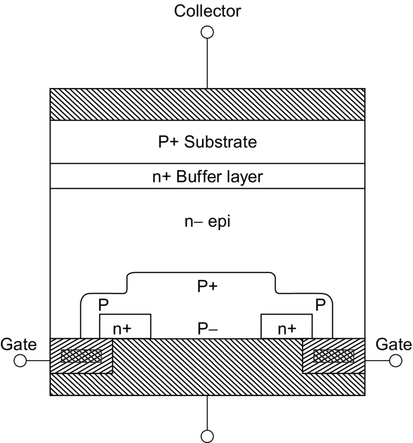
The insulated-gate bipolar transistor (IGBT) is a minority carrier device with high input impedance and large current-carrying capability. The IGBT combines the advantages of both power MOSFET and BJT, and it has MOS input characteristics and bipolar output characteristics. The basic structure of a power IGBT is shown in Fig. 6.15.
The IGBT is widely used in many applications of power electronics, such as motor drives, uninterruptible power supplies (UPS), and power modules, because of the following advantages:
• A very low on-state voltage drop due to conductivity modulation and very small conduction loss
• A simple gate driver circuit design due to the MOS gate structure
• A very large current-carrying capability and smaller chip size for a given conduction current
• Good forward and reverse voltage blocking capability
However, the IGBT has some drawbacks, compared with power MOSFET:
• Slow switching speed, current tailing due to carrier combination
• Latch-up issue due to the parasitic thyristor structure
The IGBT is viewed as a serial connection of a MOSFET and a P-i-N diode, and sometimes it is modeled as a wide base PNP transistor driven by a MOSFET in Darlington configuration. In the output I-V characteristics of a power IGBT, the conduction current starts flowing when the gate voltage exceeds the threshold voltage, and collector-source voltage is approximately above 0.7 V.
4. Power Thyristor
A thyristor is a power device with four alternating layers of p-type and n-type doping and can be turned on by the gate terminal but cannot be turned off by the gate [9]. It has the largest power-handling capability.
5. Power BJT
The power bipolar transistors (BJT) are conceptually the same as the small-signal BJTs. The main difference is that the active area of power BJT device is much larger resulting in a much higher current handling capability. Power BJTs also have a thick and lightly doped collector region. Such collector regions result in a large blocking voltage.
6.5.3 SiC Power Semiconductor Devices in Power Modules
In recent times, power semiconductor devices using silicon carbide (SiC), a wide bandgap material, rather than silicon have become commercially available. The SiC material has superior material properties for power electronic applications. SiC devices are starting to be used in power modules. In particular, SiC-merged barrier Schottky diodes are used to replace high-voltage P-i-N diodes. The advantage is that, unlike P-i-N diodes, SiC Schottky diodes are majority carrier devices and do not exhibit reverse recovery at turnoff. SiC MOSFETs are also being introduced in modules. Presently, the higher cost of SiC devices limits their adoption.
6.6 Thermal Management of Power Modules
6.6.1 The Purpose of Thermal Management
For a variety of system-level reasons, modern power electronic applications require compact and high-power density power converters. In order to achieve this required miniaturization, higher integration of components and higher switching frequencies, which reduce passive filtering element size, are required. The increase in switching frequency leads to increased power losses and the physical integration makes it harder to remove the loss heat generated. This creates a significant design challenge that requires careful thermal management. Additionally, in power modules, the power dissipation is concentrated inside the small power semiconductor chips, making heat removal particularly difficult. Power module datasheets specify a maximum allowable junction temperature, that is, temperature at the semiconductor chips inside the module. Exceeding this temperature will lead to module failure. Moreover, lower operating junction temperatures lead to markedly improved module reliability. The maximum junction temperature for current commercially available silicon-based power modules is around 150°C.
Another thermal concern affecting module reliability is thermal cycling, that is, the alternate heating and cooling of the module as a result of varying operating conditions. Excessive thermal cycling leads to aging and early failure of the module. In order to avoid overheating and to improve reliability, a common recommendation is that junction temperature should not exceed 125°C. Therefore, thermal management of power module is necessary to satisfy the thermal requirements described above.
6.6.2 Equivalent Thermal Network of Power Module
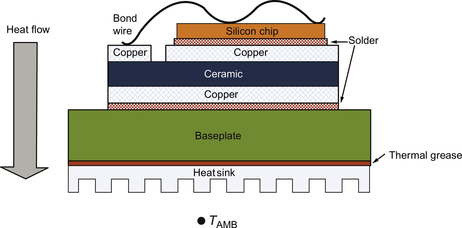
Fig. 6.16 shows a cross section of a power electronic module. Power dissipation occurs at the silicon chip due to conduction and switching losses. The heat is conducted through several material layers inside the module until it reaches the baseplate. Fig. 6.16 shows that the heat flows from top to bottom through the top solder layer, the top copper layer, the ceramic substrate, the bottom copper layer, the bottom solder layer, and the baseplate. From the baseplate, the heat exits the module, crosses the thermal grease layer, and reaches the heat sink. In case of air cooling, the heat then transfers by convection to the air surrounding the heat sink. Usually, the heat flow is modeled as being unidimensional with the lateral heat spreading modeled as a spreading angle that increases the heat flow cross section. It should be kept in mind that this approximation introduces a certain error [10]. Each material layer has a certain thermal resistance and thermal capacitance. The temperature gradient across each layer drives the conductive heat transfer. Consequently, the temperature gradually decreases from junction temperature at the silicon chip to ambient temperature TAMB.
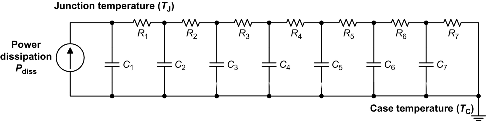
The junction temperature in the power module can be estimated by the equivalent Cauer RC thermal network shown in Fig. 6.17. In this equivalent model, voltage represents temperature, and current represents heat flow. An RC cell represents a specific material layer [11]. The thermal resistance Ri of the ith layer is given by

where di is the ith layer thickness; Ai is the effective cross-sectional area, including a spreading angle for conductors; and ki is the thermal conductivity of the ith layer.
Thermal capacitance Ci of the ith layer is given by the equation
where c is the constant pressure-specific heat capacity, ρ is the mass density, and V is the effective volume of the ith layer.
According to the equivalent thermal network, the junction temperature TJ is numerically equal to the top left node voltage (the top node of the input current source), while the case temperature TC represents the reference node voltage of the network. The power module datasheets provide a numerical value for the junction-to-case thermal resistance Rth(JC). The term “case” indicates the bottom of the baseplate, where the heat sink is attached. In the equivalent model of Fig. 6.17, Rth(JC) is equal to the sum of all thermal resistances R1 through R7. The relationship between TJ and TC is given by the following equation [12]:
This thermal resistance directly provides the temperature difference between junction and case. To calculate the absolute temperature, it is necessary to calculate the case temperature TC. This temperature can be calculated based on the selected heat sink, air flow, and ambient temperature TAMB.
As previously mentioned, power modules frequently have a thermal sensor mounted in close proximity of the chips. This gives experimental access to junction temperature in real time [13]. Note that this method can only measure the junction temperature in steady state or for slowly varying thermal transients, because the measured value is accurate only at thermal equilibrium.
According to the thermal network, the junction temperature can be controlled in an acceptable range by applying external cooling to the case of the module.
6.6.3 Cooling Solutions for Power Module
6.6.3.1 Air Cooling
The fin heat sink is a common air cooling solution used in industry, as shown in Fig. 6.18.

For low-power application, a fin heat sink with natural convection is a good choice because no additional device is needed. When the dissipated power is larger, forced convection cooling using an electric fan can be used. However, when the dissipated power density exceeds 100 W/cm2, the heat sink will not satisfy the cooling requirement, and a more effective cooling method is needed, such as liquid cooling.
6.6.3.2 Liquid Cooling
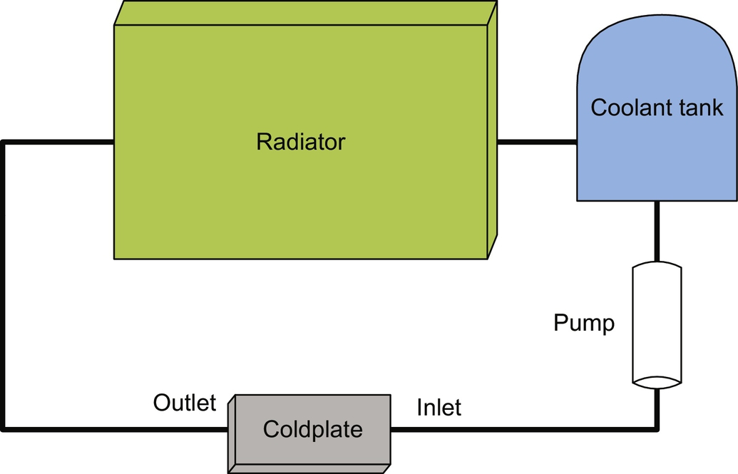
Liquid cooling has higher thermal transfer efficiency than air cooling and is used in high-power modules. The power module baseplate is thermally connected to a so-called cold plate, which is liquid-cooled. A liquid cooling system is required, as shown in Fig. 6.19. The cooling liquid in the system, such as water, is pumped into the inlet of the cold plate, is heated by the heat flow from the module, flows out from the outlet, and transfers the heat to the cooling radiator. The cold water is gathered in the coolant tank and recirculated. Liquid cooling provides superior thermal performance compared with air cooling, but it incurs additional cost and may affect reliability due to possible coolant leaks.
6.6.3.3 Double-Sided Cooling
An approach to increase cooling performance is to remove heat from both sides of the semiconductor dies, instead of removing it from one side only. This approach cannot be used effectively in case of the wire bond package of Fig. 6.16, because the wire bonds prevent heat removal from the top. Consequently, double-sided cooling can be applied only to wire-bond-free power modules. Wire-bond-free packaging techniques include low-temperature attach using double-sided DBC, flip chip solder balls interconnection technology, and press-pack technology. Design complexity, cooling efficiency, electric isolation, and power density must be considered for each case when interfacing the device package with advanced double-sided cooling schemes. The cooling methods are different and depend on the packaging technology used. The double-sided cooling methods are now briefly discussed for the double-sided DBC structure and for the press-pack structure.
6.6.3.4 Double-Sided Cooling Using the DBC Structure
Low-temperature attach techniques have been used to connect IGBT devices to DBC on both sides in order to achieve double-sided liquid cooling. This technique increases cooling performance, but electric isolation via DBC adds thermal resistance. Fig. 6.20 shows a cross section of the double-sided cooling structure with power semiconductors. This package design gave a thermal resistance of 0.087°C/W for a flow rate of 1.6 gal/min [14].
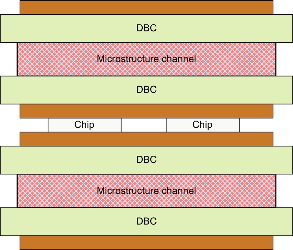
Flip chip solder ball interconnection technology can be used to eliminate cooling interface issues related to wire bonds, but electric isolation requirements limit the efficiency of the cooling system also in this case. Microchannels are integrated directly in the package to provide double-sided cooling. The interface between the device and DBC via solder balls as well as the use of DBC as isolation between the device and heat sinks somewhat reduces the heat transfer from the chip. This cooling and package configuration provides a thermal resistance of 0.09–0.12°C/W for a flow rate range of 0.2–2 gal/min [14]. Fig. 6.21 shows a cross section of the structure.

6.6.3.5 Double-Sided Cooling Using the Press-Pack Structure
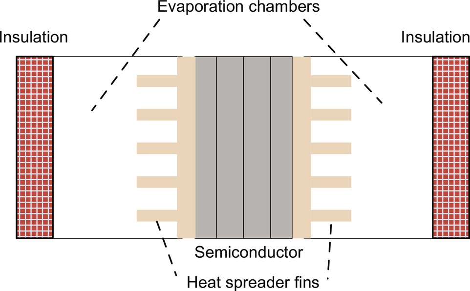
Press-pack semiconductor packaging technology can also allow advanced double-side cooling schemes. This example uses evaporators on both sides of the semiconductors. This method is promising for applications that use press-pack technology. Fig. 6.22 shows the cross section of the press-pack and double-sided multiphase cooling structure.
6.7 Reliability of Power Modules
For power electronic applications, reliability of power modules is an important issue. The reliability of power electronics has been improving over the years. As an example, power module failure rate in traction has decreased from 1000 FITs in 1995 to 20 FITs in 2000 (1 FIT=one failure per 109 device hours). In recent years, many failure-detecting tests have been proposed or improved, such as solder cracking and bond wire lift-off tests [15].
Thermomechanical stress on power module packaging materials is the most common reason for module failure due to mismatch in the coefficients of thermal expansion (CTE) between different adjacent materials inside the power module package. The structure of a power module, shown in Fig. 6.5, has been described earlier. The most common module failures are due to wire bond lifting, that is, the wire bond detaching from the surface it was bonded to, and solder cracking.
Bond wire lifting is one of the main reasons for power electronic module failures: a crack is formed and grows at the junction between the chip and the bond wire due to mismatch between the CTEs as a result of temperature variations. The difference in the CTEs causes strain at the interface. The strain initiates the crack that grows as a result of successive stress cycles during operation. This is shown in Fig. 6.23. The bond wire lifting failures can be examined by microstructural testing. A discussion of reliability in power modules can be found in [16].
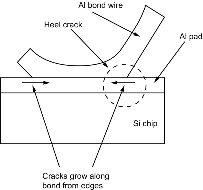
Cracks usually grow from the two end sides during thermal cycles, and the bond wire lifts up when the crack reaches the center. A contributing factor to bond wire failures is magnetic forces induced on the wire bonds by inductive coupling among bond wires.
The second most common failure is related to solder fatigue at a solder joint inside the power module. For example, a failure may occur in the solder joint between a silicon die and the copper substrate, as shown in Fig. 6.24. The failure occurs because of CTE mismatch between the die chip and the substrate, which results in mechanical stress that shifts the solder layers laterally in relation to each other and eventually creates voids.
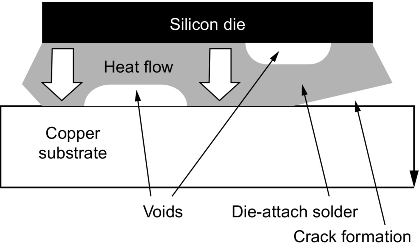
As shown in Fig. 6.24, the voids are a barrier to heat conduction from die to substrate and cause a nonuniform heat distribution. This in turn increases the thermal resistance between die and substrate and damages the die. The stress on the interfaces depends on temperature and increases as temperature increases.
Two different types of thermal stress can be identified, power cycling and thermal cycling. Power cycling refers to temperature variations caused by varying power loss in the devices due to a variation of operating conditions. Thermal cycling is the effect of temperature variations in the environment around the power module.
Power converters usually undergo both types of temperature cycling but with different levels of temperature variation and frequency [16].
6.7.1 Reliability Tests [17]
A power module is exposed to active temperature cycles due to its operation and to passive temperature cycles due to variation of the surrounding environment. Thermal cycling and power cycling tests can be performed to represent these conditions and evaluate reliability:
6.7.1.1 Thermal Cycling Test
In this test, the temperature of the power module is changed as a result of a change in case temperature or of variation of ambient temperature (TST, thermal shock test). No electric stress is applied. This test evaluates lifetime of the solder joints and ability of the device to survive sudden temperature variation.
6.7.1.2 Power Cycling Test
In this test, the ruggedness of semiconductor devices such as IGBTs and MOSFETs is evaluated under thermomechanical stress due to power loss cycling in the internal semiconductor dies. The variation of temperature is due to periodic variations of load current. This test evaluates reliability under high-temperature operation.
The equivalent test cycles can be evaluated by converting the thermal stress on solder and bond joints due to active and passive thermal stress into reliability test data.
6.8 Design Guidelines and Considerations
In order to utilize a commercially available power module to realize a switching converter for a specific application, the following steps should be followed:
1. Power module selection based on switching converter specifications. A power module of the desired topology with the appropriate voltage and current rating should be selected. The type (IGBT, MOSFET, and so on) and characteristics of the power semiconductor devices in the module determine achievable switching frequency. From the manufacturer's datasheets, conduction and switching losses can be estimated.
2. Electric design. Referring to Fig. 6.4, the external components required to realize the converter need to be designed. These include bypass capacitor CBYPASS, gate drivers (unless they are already integrated inside the module), power inductor L, and converter control. Some special considerations regarding the first two items, which are specific to power modules, will be discussed below.
3. Thermal design. Based on the estimated losses, the thermal design must be completed. The cooling method—natural convection, forced convection, or liquid cooling—is selected and the thermal circuit designed to achieve a desired maximum junction temperature under worst-case conditions.
For a successful design, it is critical to follow the specifications and recommendations in the manufacturer's datasheets. Manufacturers also provide additional design support, such as application notes, technical papers, and online loss calculation software tools for their products.
6.8.1 Bypass Capacitor Considerations
Besides component selection, as is frequently the case in power electronics, proper physical layout is critical. As shown in Fig. 6.25, for the case of a half-bridge converter, the switching loop should be minimized in physical size in order to reduce overshoot and ringing during switching. The objective is to reduce the distributed parasitic inductance of the switching loop, shown as lumped inductance LSWITCH in the figure.
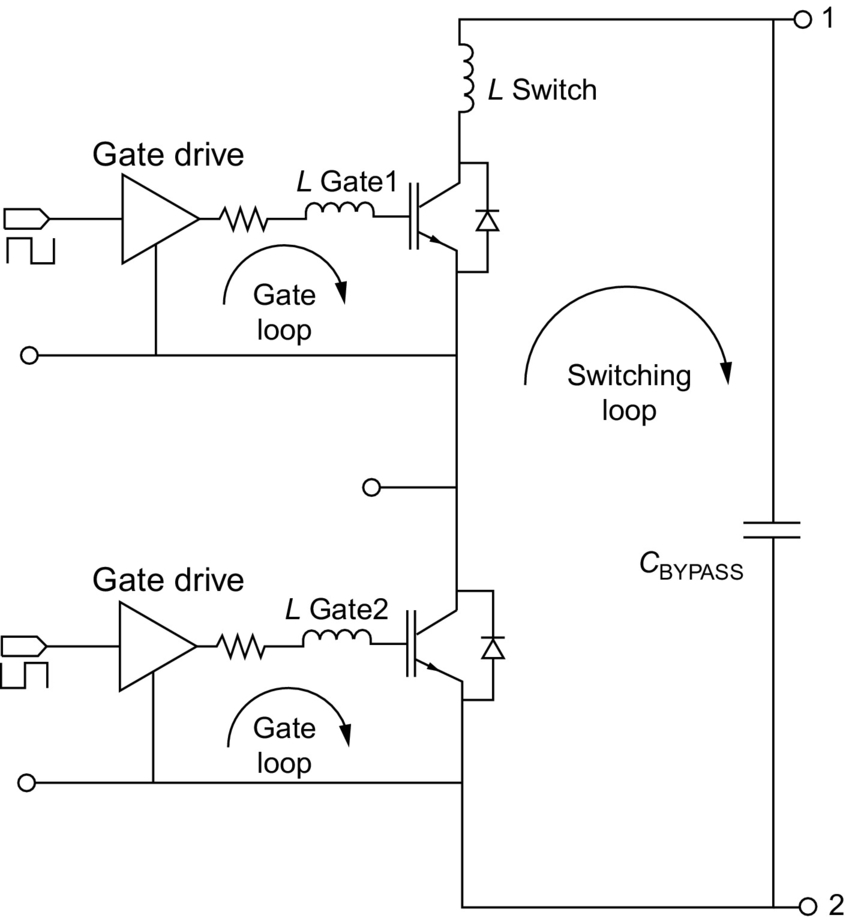
As shown in Fig. 6.4, the switching loop is partially inside the power module, but it is completed by the external capacitor CBYPASS. This capacitor should absorb the square-wave current at the switching frequency resulting from switching converter operation. It is critical to use a high-frequency high-current-ripple capacitor. Ceramic or metal film capacitors are appropriate. Polypropylene capacitors are a popular choice. It is critical to mount the bypass capacitor physically close to the module. A laminated bus bar is recommended to reduce parasitic inductance by having closely spaced flat conductors conducting opposite polarity currents.
6.8.2 Gate Driver Design Considerations
The gate driver design is similar to what is commonly done for discrete power semiconductor devices. Based on the total gate charge QG from the datasheets and on the desired gate voltage rise and fall time, a gate driver with adequate current capability is selected. The choice of gate resistor is a trade-off: a smaller gate resistor gives faster switching speed with lower switching losses and with increased gate noise immunity, whereas a larger gate resistor gives slower switching speed with reduced switching noise and reduced diode reverse recovery. It should be kept in mind that power modules frequently have internal gate resistances in case of multiple paralleled dies as shown in Fig. 6.26. Resistances Rg are internal to the module and are needed to ensure dynamic current balance. If a single gate resistor was used, there could be an LC oscillation caused by the input capacitances of the two IGBTs resonating with the parasitic inductance of the gate connection. In the case of Fig. 6.26, this resonant path has a 2Rg series damping resistance. The module datasheets usually provide a recommended external gate resistor range of values.

Regarding layout, it is important to minimize the gate loops shown in Fig. 6.25. A large gate loop causes a large parasitic inductance LGATE that resonates with the IGBT input capacitance causing gate voltage ringing, which may cause spurious IGBT switching. The power module gate contacts should be directly connected to the gate driver printed circuit board if possible.
6.8.3 Gate Kelvin Contacts
Power modules typically have gate Kelvin contacts. It is essential that they be used for the gate drive as shown in Fig. 6.4 in order to have an effective dynamic gate voltage control. Fig. 6.27 shows the case of no emitter Kelvin contact. As a result, there is a parasitic emitter inductance LE that is part of both the switching loop and the gate loop (refer to Fig. 6.25). This inductance conducts the full collector current. During turn-on, the gate drive voltage increases, and the IGBT gradually turns on. The increasing collector current induces a positive voltage vLE on the parasitic emitter inductance that subtracts from the gate driver voltage and slows down the gate-emitter voltage rise. This negative feedback effect is undesirable because it slows down the switching transition and causes the gate driver to have less dynamic control of the actual gate-emitter voltage. A similar negative feedback effect occurs at turnoff, slowing down this transition as well. This problem can be solved by providing a separate emitter Kelvin contact as shown in Fig. 6.28. The power contact emitter inductance (in red) is not part of the gate loop, and the negative feedback effect is eliminated.


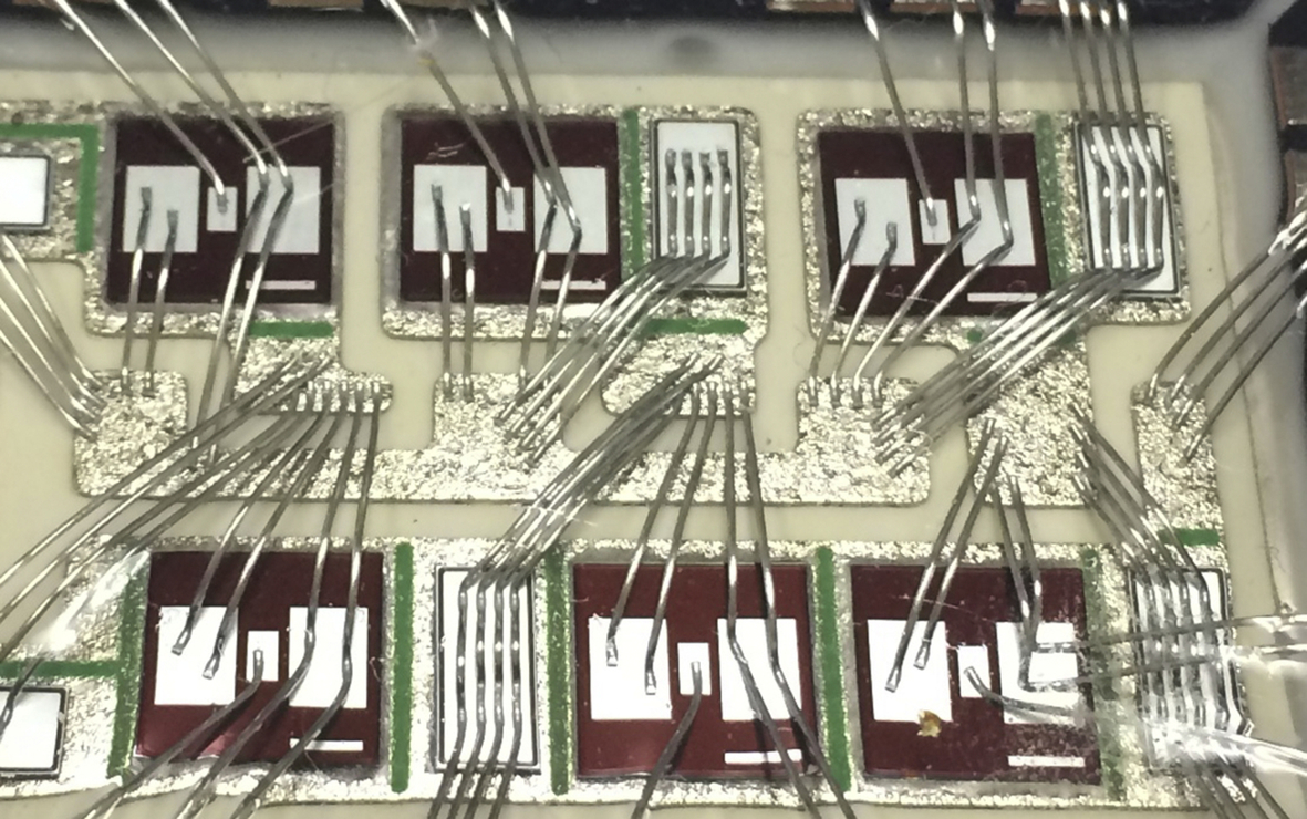
Fig. 6.29 shows the inside of a six-pack IGBT power module. On the bottom left side, one can see the power emitter pin and the Kelvin emitter pin. Notice that dedicated wire bonds go from the IGBT chip to the Kelvin emitter pin. These wire bonds conduct only the gate driver current and not the collector current and represent the E2 connection of Fig. 6.28. The figure also shows the IGBT and diode dies, the IGBT gate and emitter pads, the wire bonds, the top copper layer, the ceramic substrate, and the thermistor.

6.8.4 Other Design Considerations
In order to realize a switching converter, other design aspects must be considered, such as protection, sensing, and control implementation. The gate driver may include protections, such as short circuit protection. Current sensing may be implemented for protection and for current mode programming control. Voltage sensing is typically required for control. Either an analog or a digital controller can be used. Snubbers and clamps may be required to reduce switching waveform overshoot and ringing. EMI filters may be required.