Single-Phase Controlled Rectifiers
Kishore N. Mude University of Porto, Porto, Portugal
Amrita Vishwa Vidyapeetham University, Bengaluru, India
Abstract
In this chapter, the various topologies of single-phase controlled rectifier are presented. In the first part of the chapter, topologies pertaining to low switching frequency such as half-wave, biphase, and full-wave rectifier with source inductance are presented. In the later parts, the various concepts and topologies pertaining to active rectification are presented. The performance issues pertaining to input currents, power factor, and commutation problems in control rectifier are addressed. The various topologies of unity-power-factor rectifiers, synchronous rectifiers, and rectifier using matrix converter are presented.
Keywords:
Line-commutated control rectifiers; Unity-power-factor rectifiers; Active rectification; Synchronous rectifier
8.1 Introduction
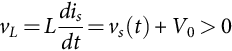
This chapter is dedicated to single-phase controlled rectifiers, which are used in a wide range of applications. As shown in Fig. 8.1, single-phase rectifiers can be classified into two big categories:
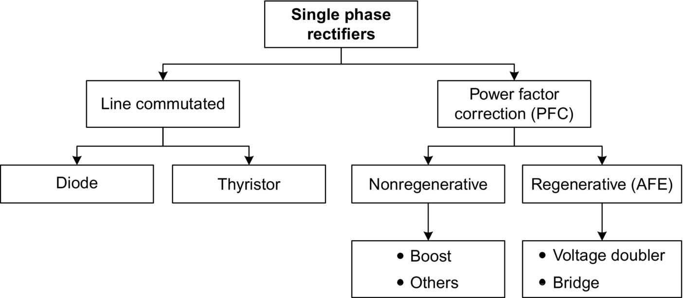
(i) Topologies working with low switching frequency, also known as line-commutated or phase controlled rectifiers
(ii) Circuits working with high switching frequency, also known as power factor correctors (PFCs), synchronous rectifiers
Line-commutated rectifiers with diodes, covered in a previous chapter of this handbook, do not allow the control of power being converted from ac to dc. This control can be achieved with the use of thyristors. These controlled rectifiers are addressed in the first part of this chapter.
In the last years, increasing attention has been paid to the control of current harmonics present at the input side of the rectifiers, originating from a very important development in the so-called PFCs and synchronous rectifiers. These circuits use power transistors working with high switching frequency to improve the waveform quality of the input current, increasing the power factor. High-power-factor rectifiers can be classified in regenerative and nonregenerative topologies. The synchronous rectification (SR) uses MOSFETs to achieve the rectification function typically performed by diodes. SR improves efficiency, thermal performance, power density, manufacturability, and reliability and decreases the overall system cost of power supply systems. New topology of control rectifier using the single-phase matrix converter is also covered in the second part of this chapter.
8.2 Line-Commutated Single-Phase Controlled Rectifiers
8.2.1 Single-Phase Half-Wave Rectifier
The single-phase half-wave rectifier uses a single thyristor to control the load voltage as shown in Fig. 8.2. The thyristor will conduct, on-state, when the voltage vT is positive and a firing current pulse iG is applied to the gate terminal. The control of the load voltage is performed by delaying the firing pulse by an angle α. The firing angle α is measured from the position where a diode would naturally conduct. In case of Fig. 8.2, the angle α is measured from the zero-crossing point of the supply voltage vs. The load in Fig. 8.2 is resistive, and therefore, the current id has the same waveform of the load voltage. The thyristor goes to the nonconducting condition, off-state, when the load voltage and consequently the current reach a negative value.

The load average voltage is given by [1]
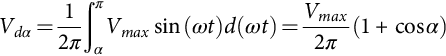
where Vmax is the supply peak voltage. Hence, it can be seen from Eq. (8.1) that changing the firing angle α controls both the load average voltage and the amount of transferred power.
Fig. 8.3A shows the rectifier waveforms for an R-L load. When the thyristor is turned on, the voltage across the inductance is

where vR is the voltage in the resistance R, given by vR=R⋅id. If vs−vR>0, from Eq. (8.2) holds that the load current increases its value. On the other hand, id decreases its value when vs−vR<0. The load current is given by
Graphically, Eq. (8.3) means that the load current id is equal to zero when A1=A2, maintaining the thyristor in conduction state even when vs<0.
When an inductive-active load is connected to the rectifier, as illustrated in Fig. 8.3B, the thyristor will be turned on if the firing pulse is applied to the gate when vs>Ed. Again, the thyristor will remain in the on-state until ![]() . When the thyristor is turned off, the load voltage will be
. When the thyristor is turned off, the load voltage will be ![]() .
.
8.2.2 Bi-Phase Half-Wave Rectifier
The biphase half-wave rectifier, shown in Fig. 8.4, uses a center-tapped transformer to provide two voltages v1 and v2. These two voltages are 180 degrees out of phase with respect to the midpoint neutral N. In this scheme, the load is fed via thyristors T1 and T2 during each positive cycle of voltages v1 and v2, respectively, while the load current returns via the neutral N.

As illustrated in Fig. 8.4, thyristor T1 can be fired into the on-state at any time, while voltage ![]() . The firing pulses are delayed by an angle α with respect to the instant where diodes would conduct. Also the current paths for each conduction state are presented in Fig. 8.4. Thyristor T1 remains in the on-state until the load current tends to a negative value. Thyristor T2 is fired into the on-state when
. The firing pulses are delayed by an angle α with respect to the instant where diodes would conduct. Also the current paths for each conduction state are presented in Fig. 8.4. Thyristor T1 remains in the on-state until the load current tends to a negative value. Thyristor T2 is fired into the on-state when ![]() , which corresponds in Fig. 8.4 to the condition when
, which corresponds in Fig. 8.4 to the condition when ![]() .
.
The mean value of the load voltage with resistive load is determined by
The ac supply current is equal to ![]() when T1 is in the on-state and
when T1 is in the on-state and ![]() when T2 is in the on-state, where N2/N1 is the transformer turns ratio.
when T2 is in the on-state, where N2/N1 is the transformer turns ratio.
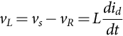
The effect of the load time constant ![]() on the normalized load current id(t)/îR(t) for a firing angle
on the normalized load current id(t)/îR(t) for a firing angle ![]() is shown in Fig. 8.5. The ripple in the load current reduces as the load inductance increases. If the load inductance
is shown in Fig. 8.5. The ripple in the load current reduces as the load inductance increases. If the load inductance ![]() , then the current is perfectly filtered.
, then the current is perfectly filtered.
8.2.3 Single-Phase Bridge Rectifier
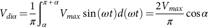
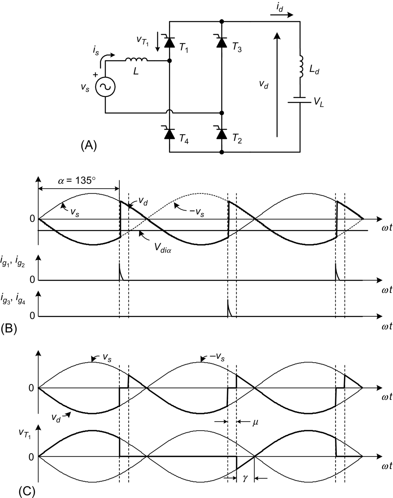
Fig. 8.6A shows a fully controlled bridge rectifier, which uses four thyristors to control the average load voltage. In addition, Fig. 8.6B shows the half-controlled bridge rectifier that uses two thyristors and two diodes.
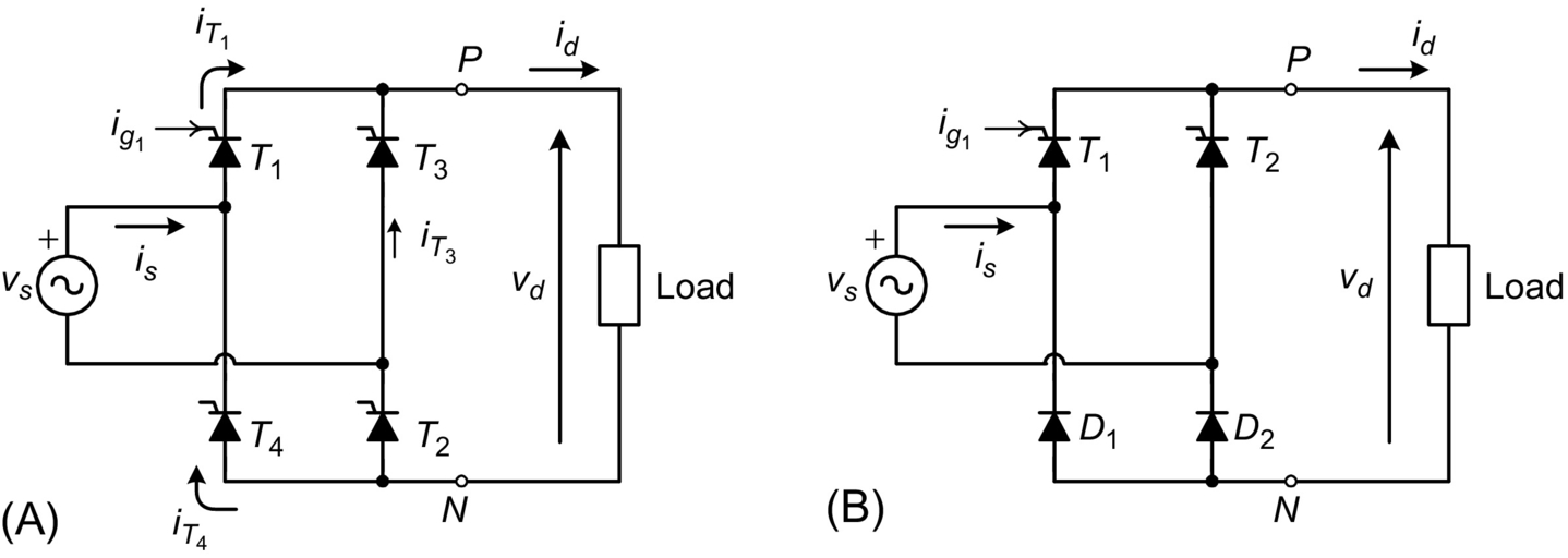
The voltage and current waveforms of the fully controlled bridge rectifier for a resistive load are illustrated in Fig. 8.7. Thyristors T1 and T2 must be fired on simultaneously during the positive half wave of the source voltage vs, to allow the conduction of current. Alternatively, thyristors T3 and T4 must be fired simultaneously during the negative half wave of the source voltage. To ensure simultaneous firing, thyristors T1 and T2 use the same firing signal. The load voltage is similar to the voltage obtained with the biphase half-wave rectifier. The input current is given by

and its waveform is shown in Fig. 8.7.
Fig. 8.8 presents the behavior of the fully controlled rectifier with resistive-inductive load (with ![]() ) [2] . The high load inductance generates a perfectly filtered current, and the rectifier behaves like a current source. With continuous load current, thyristors T1 and T2 remain in the on-state beyond the positive half wave of the source voltage vs. For this reason, the load voltage vd can have a negative instantaneous value. The firing of thyristors T3 and T4 has two effects:
) [2] . The high load inductance generates a perfectly filtered current, and the rectifier behaves like a current source. With continuous load current, thyristors T1 and T2 remain in the on-state beyond the positive half wave of the source voltage vs. For this reason, the load voltage vd can have a negative instantaneous value. The firing of thyristors T3 and T4 has two effects:

 ).
).(i) They turn off thyristors T1 and T2.
(ii) After the commutation, they conduct the load current.
This is the main reason why this type of converters is called “naturally commutated” or “line-commutated” rectifiers. The supply current iS has the square waveform, as shown in Fig. 8.9, for continuous conduction. In this case, the average load voltage is given by

8.2.4 Analysis of the Input Current
Considering a very high inductive load, the input current in a bridge-controlled rectifier is filtered and presents a square waveform. In addition, the input current is is shifted by the firing angle α with respect to the input voltage vs, as shown in Fig. 8.9A. The input current can be expressed as a Fourier series, where the amplitude of the different harmonics is

where n is the harmonic order. The root mean square (rms) value of each harmonic can be expressed as
Thus, the rms value of the fundamental current is1 is
It can be observed from Fig. 8.9A that the displacement angle ϕ1 of the fundamental current is1 corresponds to the firing angle α. Fig. 8.9B shows that in the harmonic spectrum of the input current, only odd harmonics are present with decreasing amplitude while the frequency increases. Finally, the rms value of the input current is is
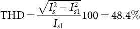
The total harmonic distortion (THD) of the input current can be determined by [3]
8.2.5 Power Factor of the Rectifier
The displacement factor of the fundamental current, obtained from Fig. 8.9A, is
In the case of nonsinusoidal currents, the active power delivered by the sinusoidal single-phase supply is
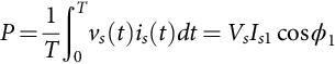
where Vs is the rms value of the single-phase voltage vs.
The apparent power is given by
The power factor (PF) is defined by

Substitution from Eqs. (8.12), (8.13), and (8.14) in Eq. (8.15) yields

This equation shows clearly that due to the nonsinusoidal waveform of the input current, the power factor of the rectifier is negatively affected both by the firing angle α and by the distortion of the input current. In effect, an increase in the distortion of the current produces an increase in the value of Is in Eq. (8.16), which deteriorates the power factor.
8.2.6 The Commutation of the Thyristors
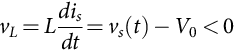
Until now, the current commutation between thyristors has been considered to be instantaneous. This condition is not valid in real cases due to the presence of the line inductance L, as shown in Fig. 8.10A. During the commutation, the current through the thyristors cannot change instantaneously, and for this reason, during the commutation angle μ, all four thyristors are conducting simultaneously. Therefore, during the commutation, the following relationship for the load voltage holds
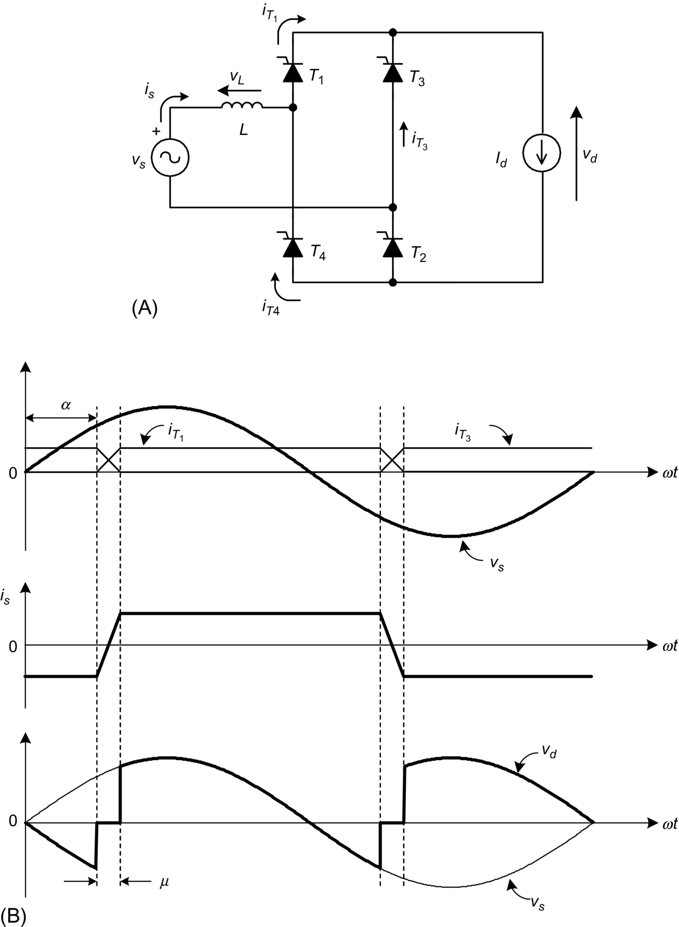
The effect of the commutation on the supply current, the voltage waveforms, and the thyristor current waveforms can be observed in Fig. 8.10B.
During the commutation, the following expression holds

Integrating Eq. (8.18) over the commutation interval yields

From Eq. (8.19), the following relationship for the commutation angle μ is obtained:
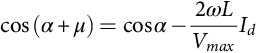
Eq. (8.20) shows that an increase of the line inductance L or an increase of the load current Id increases the commutation angle μ. In addition, the commutation angle is affected by the firing angle α. In effect, Eq. (8.18) shows that with different values of α, the supply voltage vs has a different instantaneous value, which produces different dis/dt, thereby affecting the duration of the commutation.
Eq. (8.17) and the waveform of Fig. 8.10B show that the commutation process reduces the average load voltage Vdα. When the commutation is considered, the expression for the average load voltage is given by
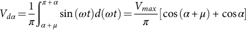
Substituting Eq. (8.20) into Eq. (8.21) yields
8.2.7 Operation in the Inverting Mode
When the angle ![]() , it is possible to obtain a negative average load voltage. In this condition, the power is fed back to the single-phase supply from the load. This operating mode is called inverter or inverting mode, because the energy is transferred from the dc to the ac side. In practical cases, this operating mode is obtained when the load configuration is as shown in Fig. 8.11A. It must be noticed that this rectifier allows unidirectional load current flow. Fig. 8.11B shows the waveform of the load voltage with the rectifier in the inverting mode, neglecting the source inductance L.
, it is possible to obtain a negative average load voltage. In this condition, the power is fed back to the single-phase supply from the load. This operating mode is called inverter or inverting mode, because the energy is transferred from the dc to the ac side. In practical cases, this operating mode is obtained when the load configuration is as shown in Fig. 8.11A. It must be noticed that this rectifier allows unidirectional load current flow. Fig. 8.11B shows the waveform of the load voltage with the rectifier in the inverting mode, neglecting the source inductance L.
Section 8.2.6 described how supply inductance increases the conduction interval of the thyristors by the angle μ. As shown in Fig. 8.11C, the thyristor voltage ![]() has a negative value during the extinction angle γ, defined by
has a negative value during the extinction angle γ, defined by
To ensure that the outgoing thyristor will recover its blocking capability after the commutation, the extinction angle should satisfy the following restriction:
where ω is the supply frequency and tq is the thyristor turn-off time. Considering Eqs. (8.23) and (8.24), the maximum firing angle is, in practice,
If the condition of Eq. (8.25) is not satisfied, the commutation process will fail, originating destructive currents.
8.2.8 Applications
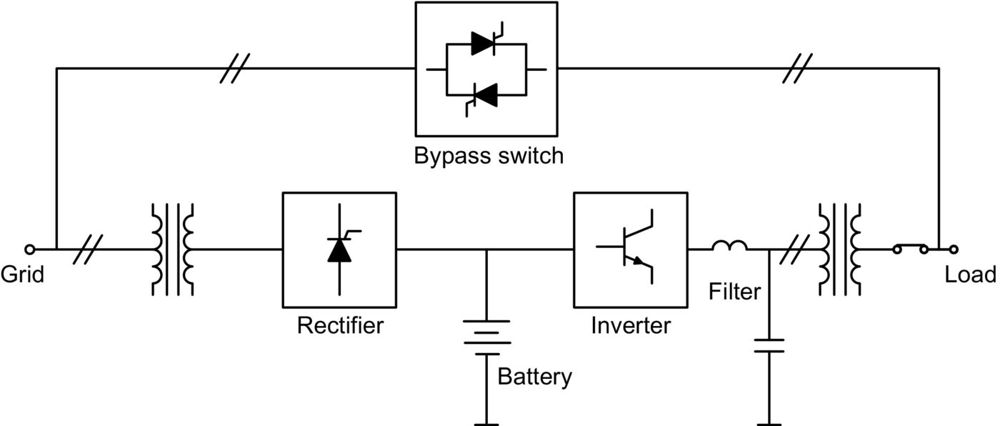
Important application areas of controlled rectifiers include uninterruptible power supplies (UPS), for feeding critical loads. Fig. 8.12 shows a simplified diagram of a single-phase UPS configuration, typically rated for <10 kVA. A fully controlled or half-controlled rectifier is used to generate the dc voltage for the inverter. In addition, the input rectifier acts as a battery charger. The output of the inverter is filtered before it is fed to the load. The operating modes of UPS are best explained in Ref. [4]. The control of low-power dc motors is another interesting application of controlled single-phase rectifiers. In the circuit of Fig. 8.13, the controlled rectifier regulates the armature voltage and consequently controls the motor current id in order to produce a required torque.
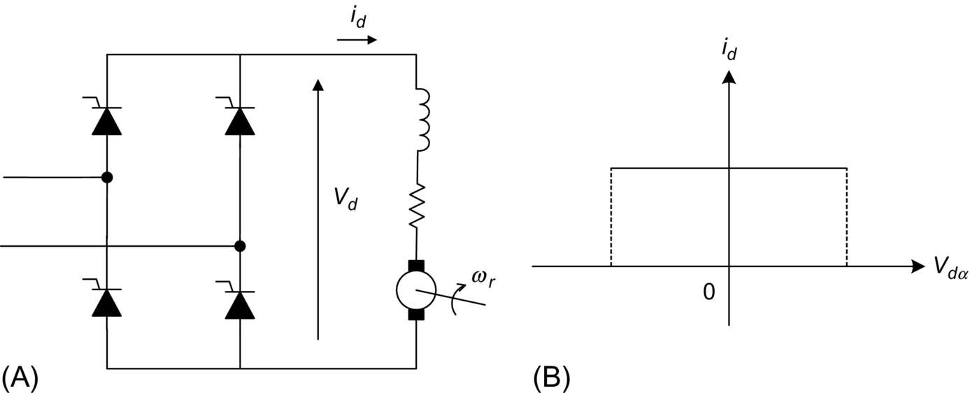
This configuration allows only positive current flow in the load. However, the load voltage can be both positive and negative. For this reason, this converter works in the two-quadrant mode of operation in the plane id vs Vdα.
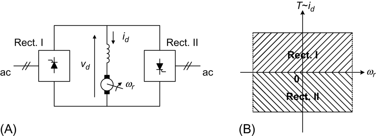
A better performance can be obtained with two rectifiers in back-to-back connection at the dc terminals, as shown in Fig. 8.14A. This arrangement, known as a dual-converter configuration, allows four-quadrant operation of the drive. Rectifier I provides positive load current id, while rectifier II provides negative load current. The motor can work in forward powering, forward braking (regenerating), reverse powering, and reverse braking (regenerating). These operating modes are shown in Fig. 8.14B, where the torque T vs the rotor speed ωr is illustrated.
8.3 Unity Power Factor Single-Phase Rectifiers
8.3.1 The Problem of Power Factor in Single-Phase Line-Commutated Rectifiers
The main disadvantages of the classical line-commutated rectifiers are that (i) they produce a lagging displacement factor with respect to the voltage of the utility and (ii) they generate an important amount of input current harmonics. These aspects have a negative influence on both power factor and power quality. In the last several years, the massive use of single-phase power converters has increased the problems of power quality in electric systems. In effect, modern commercial buildings have 50% and even up to 90% of the demand, originated by nonlinear loads, which are composed mainly of rectifiers [5,6]. Today, it is not unusual to find rectifiers with total harmonic distortion of the current ![]() , originating severe overloads in conductors and transformers.
, originating severe overloads in conductors and transformers.
Fig. 8.15A shows a single-phase rectifier with a capacitive filter, used in much of today's low-power equipment. The input current produced by this rectifier is illustrated in Fig. 8.15B; it appears highly distorted due to the presence of the filter capacitor. This current has a harmonic content shown in Fig. 8.16 and Table 8.1, with a ![]() .
.
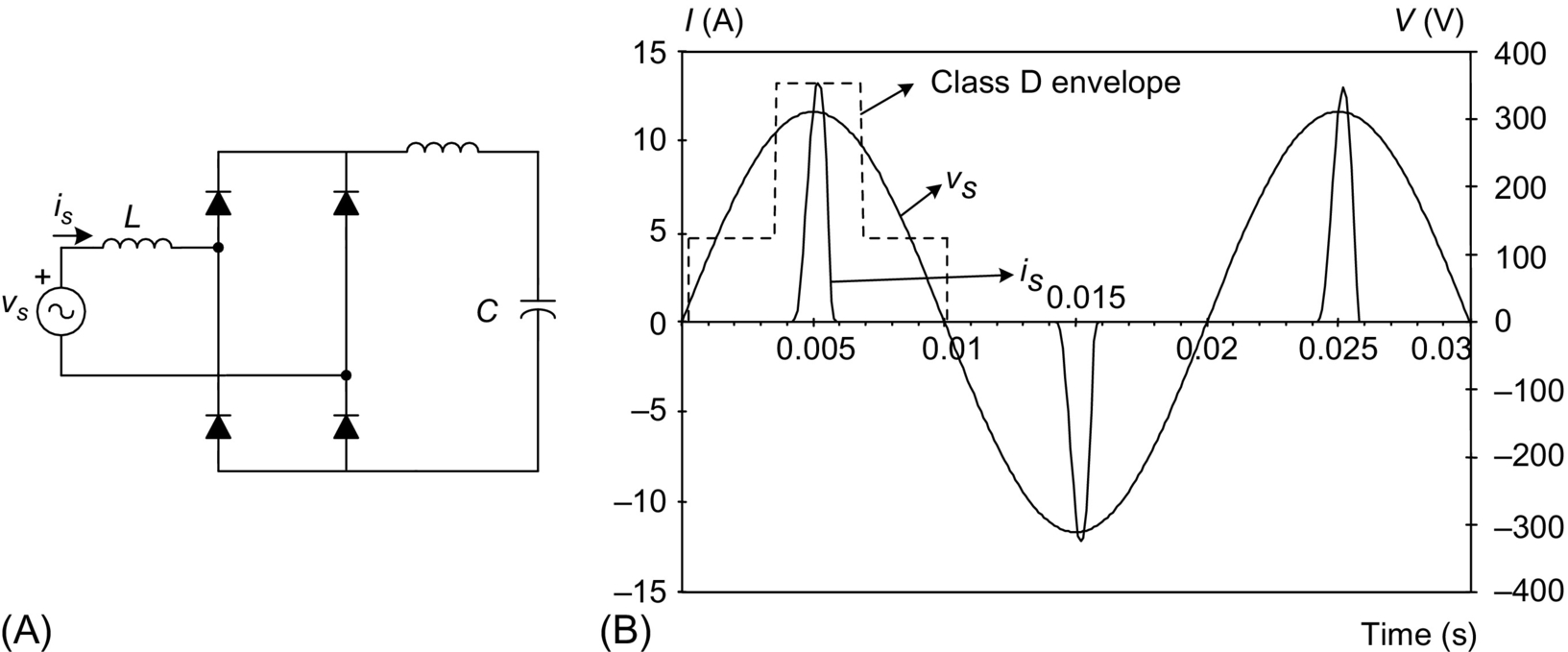

Table 8.1
Harmonic Content of the Current of Fig. 8.15
| n | 3 | 5 | 7 | 9 | 11 | 13 | 15 | 17 | 19 | 21 |
| In/I1 (%) | 96.8 | 90.5 | 81.7 | 71.0 | 59.3 | 47.3 | 35.7 | 25.4 | 16.8 | 10.6 |
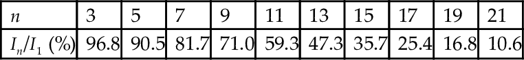
The rectifier in Fig. 8.15 has a very low power factor of ![]() , due mainly to its large harmonic content.
, due mainly to its large harmonic content.
8.3.2 Standards for Harmonics in Single-Phase Rectifiers
The relevance of the problems originated by harmonics in single-phase line-commutated rectifiers has motivated some agencies to introduce restrictions to these converters. The IEC 61000-3-2 [7], Class D International Standard, establishes limits to all low-power single-phase equipment having an input current with a “special wave shape” and an active input power ![]() . Class D equipment has an input current with a special wave shape contained within the envelope given in Fig. 8.15B. This class of equipment must satisfy certain harmonic limits, shown in Fig. 8.16. It is clear that a single-phase line-commutated rectifier with the parameters shown in Fig. 8.15A is not able to comply with the standard IEC 61000-3-2 Class D. The standard can be satisfied only by adding huge passive filters, which increases the size, weight, and cost of the rectifier. This standard has been the motivation for the development of active methods to improve the quality of the input current and, consequently, the power factor.
. Class D equipment has an input current with a special wave shape contained within the envelope given in Fig. 8.15B. This class of equipment must satisfy certain harmonic limits, shown in Fig. 8.16. It is clear that a single-phase line-commutated rectifier with the parameters shown in Fig. 8.15A is not able to comply with the standard IEC 61000-3-2 Class D. The standard can be satisfied only by adding huge passive filters, which increases the size, weight, and cost of the rectifier. This standard has been the motivation for the development of active methods to improve the quality of the input current and, consequently, the power factor.
8.3.3 The Single-Phase Boost Rectifier
One of the most important high-power-factor rectifiers, from a theoretical and conceptual point of view, is the so-called single-phase boost rectifier, shown in Fig. 8.17A, which is obtained from a classical noncontrolled bridge rectifier, with the addition of transistor T, diode D, and inductor L.

8.3.3.1 Working Principle, Basic Concepts
In boost rectifiers, the input current is(t) is controlled by changing the conduction state of transistor T. When transistor T is in the on-state, the single-phase power supply is short-circuited through the inductance L, as shown in Fig. 8.17B; the diode D avoids the discharge of the filter capacitor C through the transistor. The current of the inductance iL is given by the following equation:
Due to the fact that ![]() , the on-state of transistor T always produces an increase in the inductance current iL and consequently an increase in the absolute value of the source current is.
, the on-state of transistor T always produces an increase in the inductance current iL and consequently an increase in the absolute value of the source current is.
When transistor T is turned off, the inductor current iL cannot be interrupted abruptly and flows through diode D, charging capacitor C. This is observed in the equivalent circuit of Fig. 8.17C. In this condition, the behavior of the inductor current is described by

If ![]() , which is an important condition for the correct behavior of the rectifier, then
, which is an important condition for the correct behavior of the rectifier, then ![]() , and this means that in the off-state the inductor current decreases its instantaneous value.
, and this means that in the off-state the inductor current decreases its instantaneous value.
8.3.3.2 Continuous Conduction Mode (CCM)
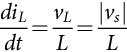
When an appropriate firing pulse sequence is applied to transistor T, the waveform of the input current is can be controlled to follow a sinusoidal reference, as can be observed in the positive half wave of is in Fig. 8.18. This figure shows the reference inductor current ![]() , the inductor current iL, and the gate drive signal x for transistor T. Transistor T is on when
, the inductor current iL, and the gate drive signal x for transistor T. Transistor T is on when ![]() , and it is off when
, and it is off when ![]() .
.
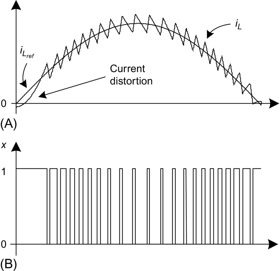
Fig. 8.18 clearly shows that the on(off)-state of transistor T produces an increase (decrease) in the inductor current iL. Note that for low values of vs, the inductor does not have enough energy to increase the current value and, for this reason, it presents a distortion in their current waveform as shown in Fig. 8.18A.
Fig. 8.19 presents a block diagram of the control system for the boost rectifier, which includes a proportional-integral (PI) controller, to regulate the output voltage vo. The reference value ![]() for the inner current control loop is obtained from the multiplication between the output of the voltage controller and the absolute value
for the inner current control loop is obtained from the multiplication between the output of the voltage controller and the absolute value ![]() . A hysteresis controller provides a fast control for the inductor current iL, resulting in a practically sinusoidal input current is.
. A hysteresis controller provides a fast control for the inductor current iL, resulting in a practically sinusoidal input current is.
Typically, the output voltage vo should be at least 10% higher than the peak value of the source voltage vs(t), in order to assure good dynamic control of the current. The control works with the following strategy: a step increase in the reference voltage ![]() will produce an increase in the voltage error
will produce an increase in the voltage error ![]() and an increase of the output of the PI controller, which originates an increase in the amplitude of the reference current
and an increase of the output of the PI controller, which originates an increase in the amplitude of the reference current ![]() . The current controller will follow this new reference and will increase the amplitude of the sinusoidal input current is, which will increase the active power delivered by the single-phase power supply, producing finally an increase in the output voltage vo.
. The current controller will follow this new reference and will increase the amplitude of the sinusoidal input current is, which will increase the active power delivered by the single-phase power supply, producing finally an increase in the output voltage vo.
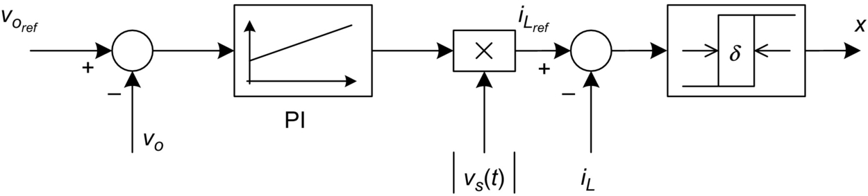
Fig. 8.20A shows the waveform of the input current is and the source voltage vs. The ripple of the input current can be reduced by shortening the hysteresis width δ. The trade-off for this improvement is an increase in the switching frequency, which is proportional to the commutation losses of the transistors. For a given hysteresis width δ, a reduction of inductance L also produces an increase in the switching frequency. As can be seen, the input current presents a third-harmonic component. This harmonic is generated by the second-harmonic component present in vo, which is fed back through the voltage (PI) controller and multiplied by the sinusoidal waveform, generating a third-harmonic component on ![]() . This harmonic contamination can be avoided by filtering the vo measurement with a low-pass filter or a band-stop filter around 2ωs. The input current obtained using the measurement filter is shown in Fig. 8.20B. Fig. 8.20D confirms the reduction of the third-harmonic component.
. This harmonic contamination can be avoided by filtering the vo measurement with a low-pass filter or a band-stop filter around 2ωs. The input current obtained using the measurement filter is shown in Fig. 8.20B. Fig. 8.20D confirms the reduction of the third-harmonic component.
However, in both cases, a drastic reduction in the harmonic content of the input current is can be observed in the frequency spectrum of Fig. 8.20C and D. This current fulfills the restrictions established by standard IEC 61000-3-2. The total harmonic distortion of the current in Fig. 8.20A is THD=7.46%, while the THD of the current of Fig. 8.20B is 4.83%; in both cases, a very high power factor, over 0.99, is reached.
Fig. 8.21 shows the dc voltage control loop dynamic behavior for step changes in the load. An increase in the load, at t=0.3 (s), produces an initial reduction of the output voltage vo, which is compensated by an increase in the input current is. At t=0.6 (s), a step decrease in the load is applied. The dc voltage controller again adjusts the supply current in order to balance the active power.

8.3.3.3 Discontinuous Conduction Mode (DCM)
This PFC method is based on an active current waveform-shaping principle. There are two different approaches considering fixed and variable switching frequency, both operating principles are illustrated in Fig. 8.22.
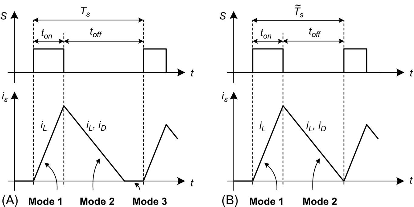
(a) DCM with fixed switching frequency
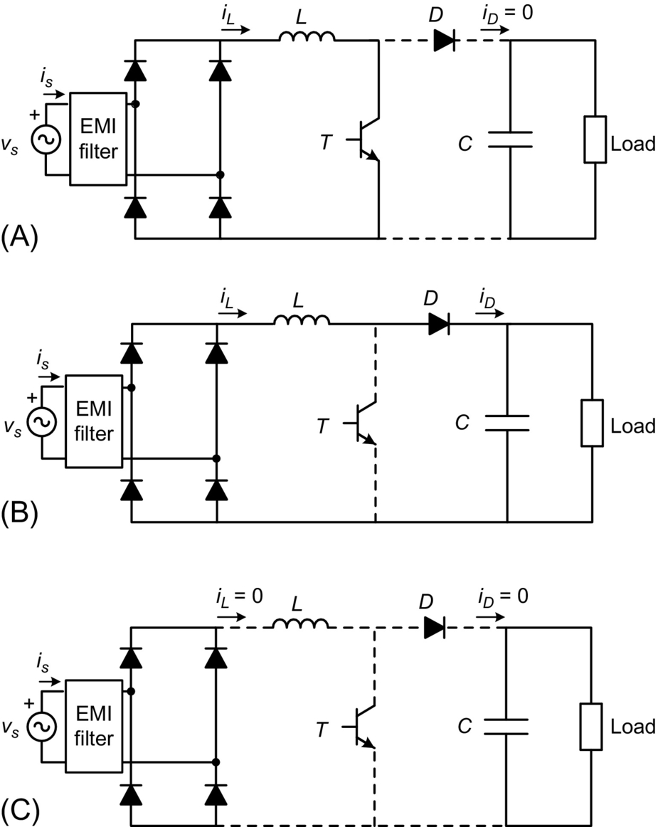
The current shaping strategy is achieved by combining three different conduction modes, performed over a fixed switching period Ts. At the beginning of each period, the power semiconductor is turned on. During the on-state, shown in Fig. 8.23A, the power supply is short-circuited through the rectifier diodes, the inductor L, and the boost switch T. Hence, the inductor current iL increases at a rate proportional to the instantaneous value of the supply voltage. As a result, during the on-state, the average supply current is is proportional to the supply voltage vs, which yields to power factor correction.
When the switch is turned off, the current flows to the load trough diode D, as shown in Fig. 8.23B. The instantaneous current value decreases (since the load voltage vo is higher than the supply peak voltage) at a rate proportional to the difference between the supply and load voltage. Finally, the last mode, illustrated in Fig. 8.23C, corresponds to the time in which the current reaches zero value, completing the switching period Ts. Therefore, the supply current is not proportional to the voltage source during the whole control period, introducing distortion and undesirable EMI in comparison with CCM.
The duty cycle ![]() is determined by the control loop, in order to obtain the desired output power and to ensure operation in DCM, that is, to reach zero current before the new switching cycle starts. The control strategy can be implemented with analog circuitry as shown in Fig. 8.24, or digitally with modern computing devices. Generally, the duty cycle is controlled with a slow control loop, maintaining the output voltage and duty cycle constant over a half-source cycle.
is determined by the control loop, in order to obtain the desired output power and to ensure operation in DCM, that is, to reach zero current before the new switching cycle starts. The control strategy can be implemented with analog circuitry as shown in Fig. 8.24, or digitally with modern computing devices. Generally, the duty cycle is controlled with a slow control loop, maintaining the output voltage and duty cycle constant over a half-source cycle.
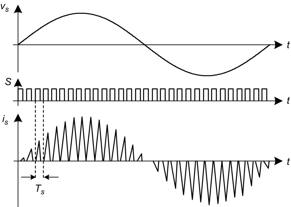
A qualitative example of the supply voltage and current obtained using DCM is illustrated in Fig. 8.25.

(b) DCM with variable switching frequency
The operating principle is similar to the one used in the previous case, the main difference is that mode 3 is avoided by switching the transistor again to the on-state, immediately after the inductor current reaches zero value. This reduces the current distortion, with the trade-off of introducing variable switching frequency (Ts is variable) and consequently lower-order harmonic content.
Both CCM and DCM achieve an improvement in the power factor. The DCM is more efficient since reverse-recovery losses of the boost diode are eliminated; however, this mode introduces high-current ripple and considerable distortion, and usually, an important fifth-order harmonic is obtained. Therefore, boost DCM applications are limited to 300 W power levels, to meet standards and regulations. The DCM with variable switching frequency reduces this harmonic content, at expends of a wide distributed current spectrum and all related design problems.
8.3.3.4 Resonant Structures for the Boost Rectifiers
An important issue in power electronics is the power losses in power semiconductors. These losses can be classified in two groups: conduction losses and switching losses, as shown in Fig. 8.26.
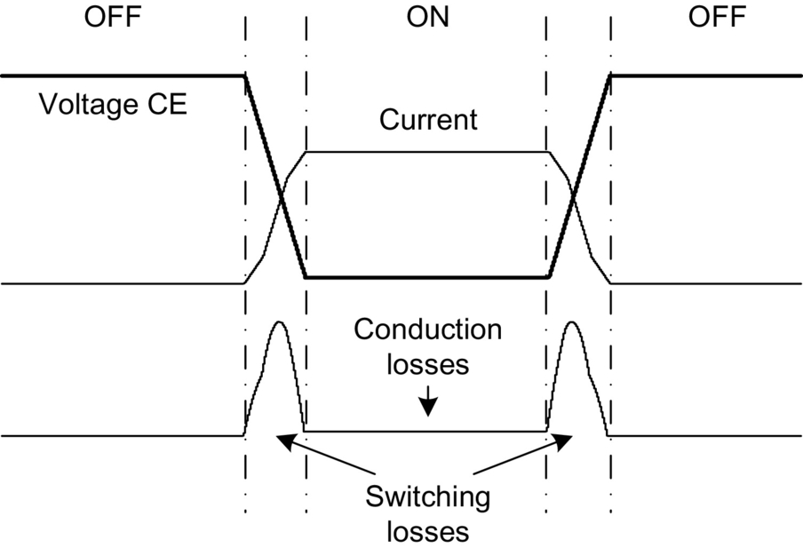
The conduction losses are produced by the current through the semiconductor juncture, so these losses are unavoidable. However, the switching losses, which are produced while the power semiconductors work in linear state during the transition from on- to off-state or from off- to on-state, can be reduced or even eliminated, if the switch (transition) occurs when (a) the current across the power semiconductor is zero or (b) the voltage between the power terminals of the power semiconductor is zero.
This operation mode is used in the so-called resonant or soft-switched converters, which are discussed in detail in a different chapter of this handbook. Resonant operation can also be used with the boost converter topology. In order to produce this condition, topology of Fig. 8.17 needs to be modified, by including reactive components and additional semiconductors.
In Fig. 8.27, a resonant structure for zero-current switching (ZCS) [8] is shown. As can be seen, additional resonant inductors (![]() and
and ![]() ), capacitors (Cr), diodes (
), capacitors (Cr), diodes (![]() and
and ![]() ), and power switch (Sr) have been included.
), and power switch (Sr) have been included.
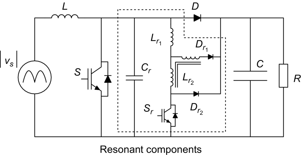
In a similar way, in Fig. 8.28, a resonant structure for zero-voltage switching (ZVS) [9] is shown. Once again, additional inductance (Lr), capacitor (Cr), and power switch (Sr) are added; note, however, that diode D has been replaced by two “resonant diodes,” ![]() and
and ![]() . In both cases, the ZVS or ZCS condition is reached through a proper control of Sr. Other resonant topologies are described in the literature [10–12] with similar behavior.
. In both cases, the ZVS or ZCS condition is reached through a proper control of Sr. Other resonant topologies are described in the literature [10–12] with similar behavior.

8.3.3.5 Bridgeless Boost Rectifier
The bridgeless boost rectifier [13] is shown in Fig. 8.29A. This rectifier replaces the input diode rectifier by a combination of two boost rectifiers that work alternately: (a) When vs is positive, T1 and D1 operate as boost rectifier 1 (Fig. 8.29B), and (b) when vs is negative, T2 and D2 operate as boost rectifier 2 (Fig. 8.29C).

This topology reduces the conduction losses of the rectifier [14,15] but requires a slightly more complex control scheme; also EMI and EMC aspects must be considered.
8.3.4 Voltage Doubler PWM Rectifier
Fig. 8.30A shows the power circuit of the voltage-doubler pulse-width-modulated (PWM) rectifier, which uses two transistors T1 and T2 and two filter capacitors C1 and C2. The transistors are switched complementary to control the waveform of the input current is and the output dc voltage vo. Capacitor voltages VC1 and VC2 must be higher than the peak value of the input voltage vs to ensure the control of the input current.
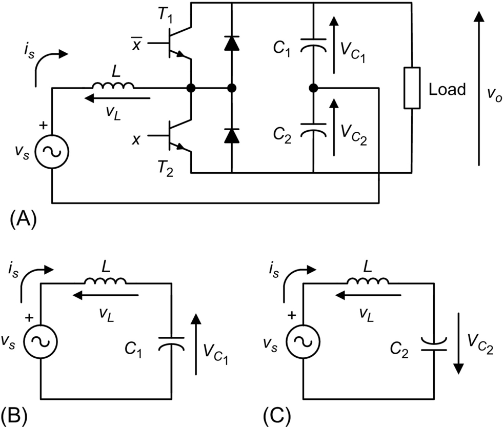
The equivalent circuit of this rectifier with transistor T1 in the on-state is shown in Fig. 8.30B. For this case, the inductor voltage dynamic equation is 10.5:
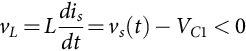
Eq. (8.28) means that under this conduction state, current is(t) decreases its value.
On the other hand, the equivalent circuit of Fig. 8.30C is valid when transistor T2 is in the conduction state, resulting in the following expression for the inductor voltage

Hence, for this condition, the input current is(t) increases.
Therefore, the waveform of the input current can be controlled by switching appropriately transistors T1 and T2 in a similar way as shown in Fig. 8.18A for the single-phase boost converter. Fig. 8.31 shows a block diagram of the control system for the voltage-doubler rectifier, which is very similar to the control scheme of the boost rectifier. This topology can present an unbalance in the capacitor voltages VC1 and VC2, which will affect the quality of the control. This problem is solved by adding to the actual current value is an offset signal proportional to the capacitor's voltage difference.

Fig. 8.32 shows the waveform of the input current. The ripple amplitude of this current can be reduced by decreasing the hysteresis width of the controller.

8.3.5 The PWM Rectifier in Bridge Connection
Fig. 8.33A shows the power circuit of the fully controlled single-phase PWM rectifier in bridge connection, which uses four transistors with antiparallel diodes to produce a controlled dc voltage vo. Using a bipolar PWM switching strategy, this converter may have two conduction states: (i) transistors T1 and T4 in the on-state and T2 and T3 in the off-state and (ii) transistors T2 and T3 in the on-state and T1 and T4 in the off-state.
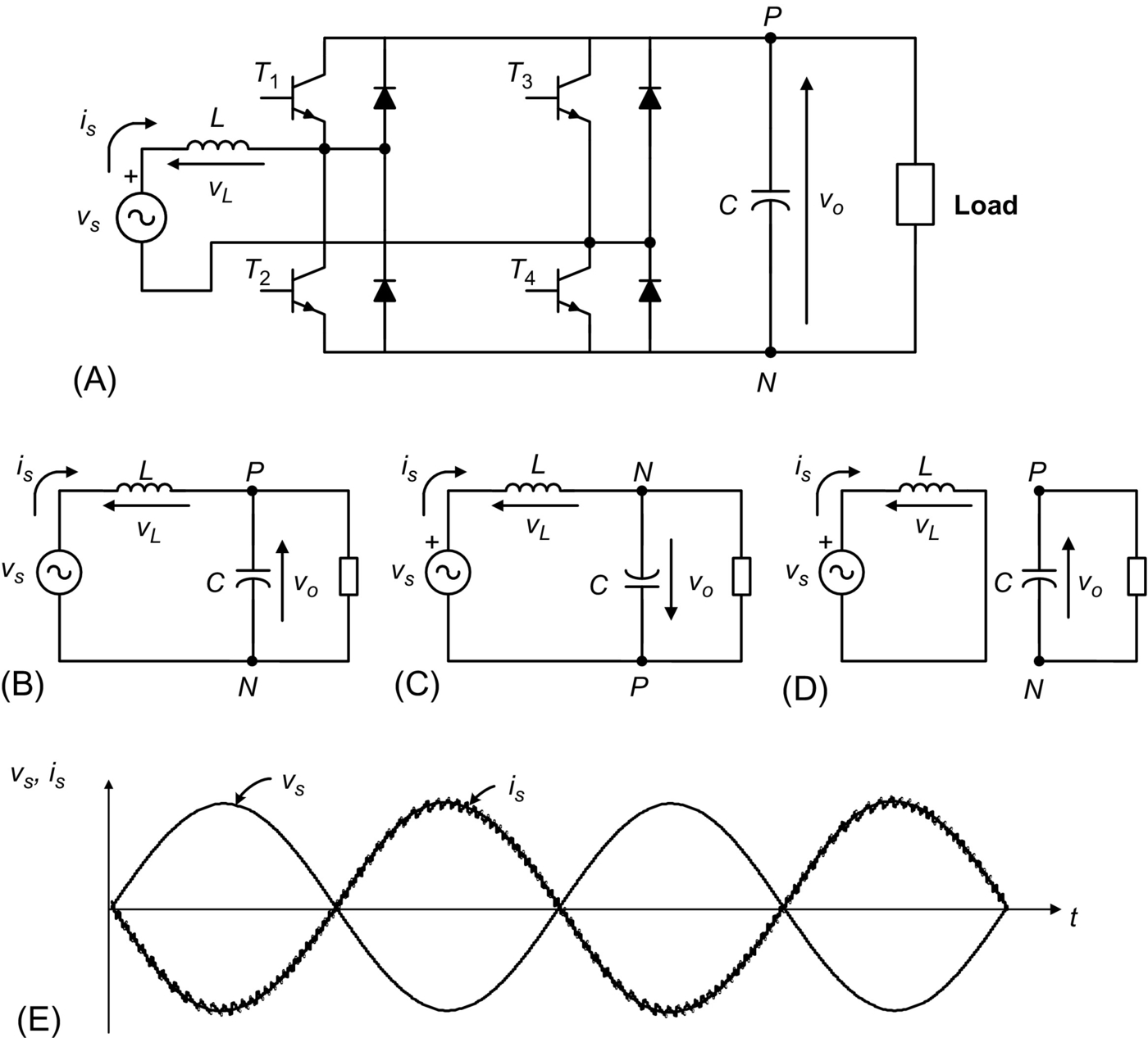
In this topology, the output voltage vo must be higher than the peak value of the ac source voltage vs, to ensure a proper control of the input current.
Fig. 8.33B shows the equivalent circuit with transistors T1 and T4 on. In this case, the inductor voltage is given by
Therefore, in this condition, a reduction of the inductor current is is produced.
Fig. 8.33C shows the equivalent circuit with transistors T2 and T3 on. Here, the inductor voltage has the following expression:
which means an increase in the instantaneous value of the input current is.
Finally, Fig. 8.33D shows the equivalent circuit with transistors T1 and T3 or T2 and T4 are in the on-state. In this case, the input voltage source is short-circuited through inductor L, which yields
Eq. (8.32) implies that the current value will depend on the sign of vs.
The waveform of the input current is can be controlled by appropriately switching transistors T1–T4 or T2–T3, originating a similar shape to the one shown in Fig. 8.18A for the single-phase boost rectifier.
The control strategy for the rectifier is similar to the one illustrated in Fig. 8.31, for the voltage-doubler topology. The quality of the input current obtained with this rectifier is the same as presented in Fig. 8.32 for the voltage-doubler configuration.
The input current waveform can be slightly improved if the state of Fig. 8.33D is used. This can be done by replacing the hysteresis current control with a more complex linear control plus a three-level PWM modulator. This method reduces the semiconductor switching frequency and provides a more defined current spectrum.
Finally, it must be said that one of the most attractive characteristics of the fully controlled PWM converter in bridge connection and the voltage doubler is their regeneration capability. In effect, these rectifiers can deliver power from the load to the single-phase supply, operating with sinusoidal current and a high power factor of ![]() . Fig. 8.33E shows that during regeneration, the input current is is 180 degrees out of phase with respect to the supply voltage vs, which means operation with power factor
. Fig. 8.33E shows that during regeneration, the input current is is 180 degrees out of phase with respect to the supply voltage vs, which means operation with power factor ![]() (PF is approximately 1 because of the small harmonic content in the input current).
(PF is approximately 1 because of the small harmonic content in the input current).
8.3.6 Applications of Unity Power Factor Rectifiers
8.3.6.1 Boost Rectifier Applications
The single-phase boost rectifier has become the most popular topology for power factor correction (PFC) in general-purpose power supplies. To reduce the costs, the complete control system shown in Fig. 8.19 and the gate drive circuit of the power transistor have been included in a single integrated circuit (IC), like the UC3854 [16] or MC33262, shown in Fig. 8.34.

Today, there is increased interest in developing high-frequency electronic ballasts to replace the classical electromagnetic ballast present in fluorescent lamps. These electronic ballasts require an ac-dc converter. To satisfy the harmonic current injection from electronic equipment and to maintain a high power quality, a high-power-factor rectifier can be used, as shown in Fig. 8.35 [17].
8.3.6.2 Voltage Doubler PWM Rectifier
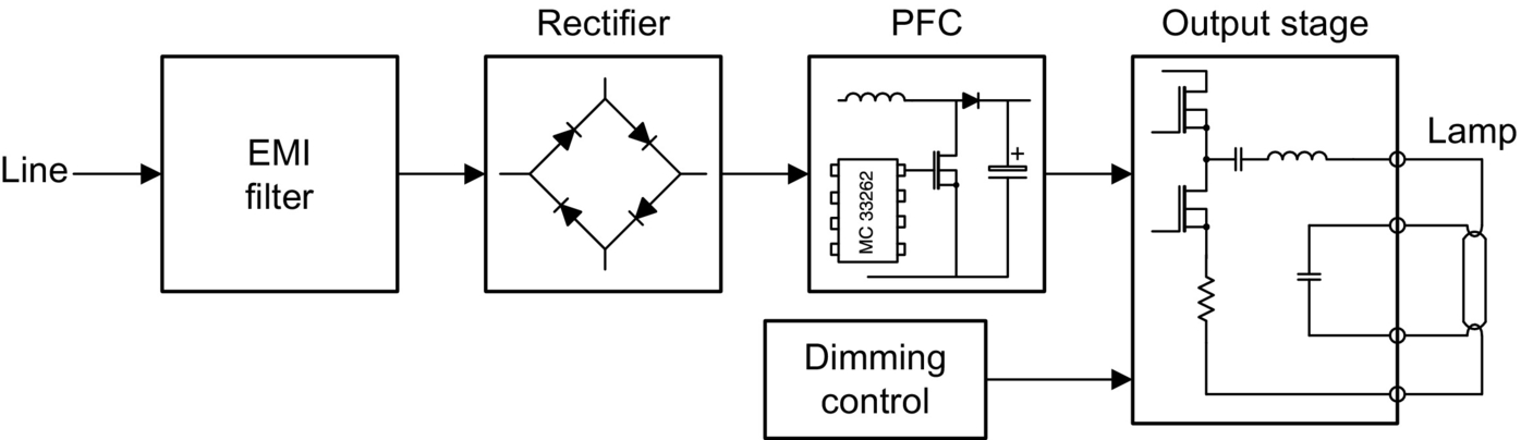
The development of low-cost compact motor drive systems is a very relevant topic, particularly in the low-power range. Fig. 8.36 shows a low-cost converter for low-power induction motor drives. In this configuration, a three-phase induction motor is fed through the converter from a single-phase power supply. Transistors T1 and T2 and capacitors C1 and C2 constitute the voltage-doubler single-phase rectifier, which controls the dc link voltage and generates sinusoidal input current, working with close-to-unity power factor [18]. On the other hand, transistors T3, T4, T5, and T6 and capacitors C1 and C2 constitute the power circuit of an asymmetrical inverter that supplies the motor. An important characteristic of the power circuit shown in Fig. 8.36 is the capability of regenerating power to the single-phase mains.
8.3.6.3 PWM Rectifier in Bridge Connection
Distortion of the input current in the line-commutated rectifiers with capacitive filtering is particularly critical in the UPS fed from motor-generator sets. In effect, due to the higher value of the generator impedance, the current distortion can originate an unacceptable distortion on the ac voltage, which affects the behavior of the whole system. For this reason, it is very attractive to use rectifiers with low distortion in the input current.
Fig. 8.37 shows the power circuit of a single-phase UPS, which has a PWM rectifier in bridge connection at the input side. This rectifier generates a sinusoidal input current and controls the charge of the battery [19].
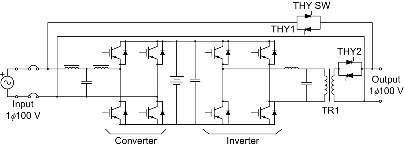
Perhaps the most typical and widely accepted area of application of high-power-factor single-phase rectifiers is in locomotive drives [20]. An essential prerequisite for proper operation of voltage-source three-phase inverter drives in modern locomotives is the use of four-quadrant line-side converters, which ensure motoring and braking of the drive, with reduced harmonics in the input current. Fig. 8.38 shows a simplified power circuit of a typical drive for a locomotive connected to a single-phase power supply [20], which includes a high-power-factor rectifier at the input.

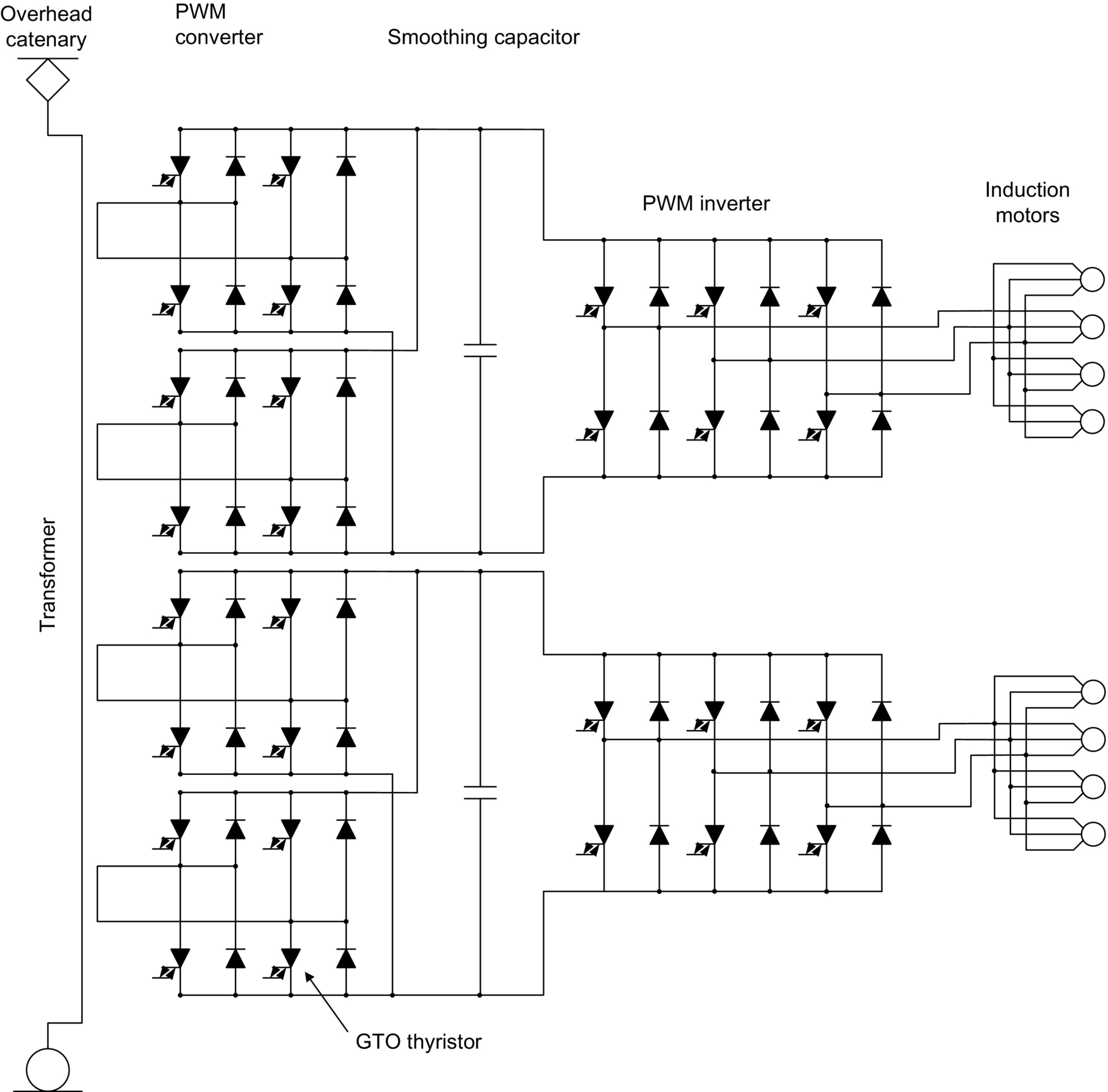
Finally, Fig. 8.39 shows the main circuit diagram of the 300 series Shinkansen train [21]. In this application, ac power from the overhead catenary is transmitted through a transformer to single-phase PWM rectifiers, which provide the dc voltage for the inverters. The rectifiers are capable of controlling the input ac current in an approximate sine waveform and in phase with the voltage, achieving power factor close to unity on powering and on regenerative braking. Regenerative braking produces energy savings and an important operational flexibility.
8.3.7 Synchronous Rectifier
The synchronous rectifier (SR) also known as active rectifier is able to reduce the losses, which lead to improvement in efficiency. The conduction loss contributes a significant role in the overall power loss of diode rectifier, especially in low-output-voltage applications. In the diode rectifier, conduction loss of diode depends on the forward voltage drop, diode resistance, and the magnitude of current that passes through the devices, while in the SR, MOSFET conduction loss depends on the on resistance (RDS,on) of the MOSFET and the current that passes through the devices. Moreover, driving loss is also a part of conduction losses in MOSFET, but it has a very less significant role as compared with total power loss. Therefore, the SR has been widely adopted in low-output-voltage applications with reducing the conduction loss of the output rectifier to improve the efficiency.
The advantages of using SR in high-performance, high-power converters include better efficiency, lower power dissipation, better thermal performance, and inherently optimal current sharing when synchronous MOSFETs are paralleled. The number of MOSFETs can be paralleled to handle higher output currents and results in less equivalent effective RDS,on. Moreover, RDS,on has a positive temperature coefficient so the MOSFETs will automatically tend to share current equally, facilitating optimal thermal distribution among the SR devices. This improves the ability to remove heat from the components and the PCB, directly improving the thermal performance of the design. Other potential benefits from SR include smaller form factors, higher ambient operating temperatures, and higher power densities. As discussed above, the downside to SRs is that they require control circuitry to ensure the devices turn on or off synchronously, that is, at the right time. Circuitry required for the control of the SR normally includes voltage and current detectors and drive circuitry for the active devices.
8.3.7.1 Operating Principle
Fig. 8.40 shows the circuit diagram of SR that consists an inductor and four transistors with their body diodes. The transistor used in the circuit must be the MOSFET that can conduct in both the direction. The operating principle of SR is based on the modes of technique to generate the gate signal. The current-driven SR has been used to generate the gate signal for the devices as this method is suitable for all types of topologies and offered number of advantages over voltage-driven method. The current-driven method senses the current flowing through the SR to turn on and turn off the SR properly. The current sensor is used to sense the input current that must flow through the devices. However, for positive half cycle of supply voltage, the current will flow (source to rectifier direction) through the MOSFETs S1 and S2, and for negative cycle of supply voltage, current will flow (rectifier to source direction) through MOSFETs S3 and S4.

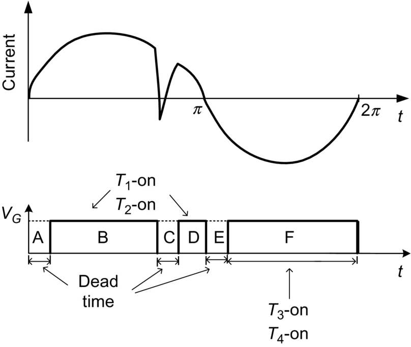
The waveforms of gate signal and dead time are shown in Fig. 8.41. At the beginning of the sinusoidal cycle, the current starts flowing in the body diode, generating a negative VDS across the MOSFET; at that point, turn-on signal is provided to the MOSFET. The dropout voltage across the device falls to much lower voltage, and MOSFET turned on as soft switching that helps to reduce the power losses and results in increasing the system efficiency. Once the MOSFET is on, it must remain in this position until the rectified current will decrease to almost zero; closer is better for the losses point of view. Therefore, a zero-crossing comparator can be used to understand when the drain-source voltage reaches the zero-voltage condition. For this purposes, the value of threshold voltage to turn off the devices must be negative and close to zero, to avoid cross conduction and reduce the body-diode conduction interval at the tail of the semisinusoid.

Let us assume that there are two situations that occur: (a) Current has a spike, and (b) current has multiple zero crossing as shown in Figs. 8.42 and 8.43, respectively. When current has a spike, sensor detects zero current, and MOSFETs S1 and S2 are turned off, and negative current flows through the body diodes. Again, current crosses the zero crossing and becomes positive, and body diodes D1 and D2 start conducting for the dead-time C as shown in Fig. 8.43. After the dead-time C, again MOSFETs. Moreover, in the case of multiple zero crossing, when the current passes from positive to negative (i.e., at point z1), sensor detects zero current, and MOSFETs S1 and S2 are turned off. The negative current flows through the body diodes D3 and D4, and again, current changes the direction, crosses the zero crossing (i.e., at point z2), and becomes positive. Then, body diodes D1 and D2 start conducting, and again, current changes the direction, crosses the zero crossing (i. e. at point z3), becomes negative, and flows through the body diodes D3 and D4, and process will have continued. In multiple zero crossing, the conduction period of body diodes either D1 and D2 or D3 and D4 is larger than dead time; then, respective MOSFETs (for instance, for diodes D1 and D2, MOSFETs S1 and S2 will conduct) will turn on, and they will conduct till the next zero crossing.

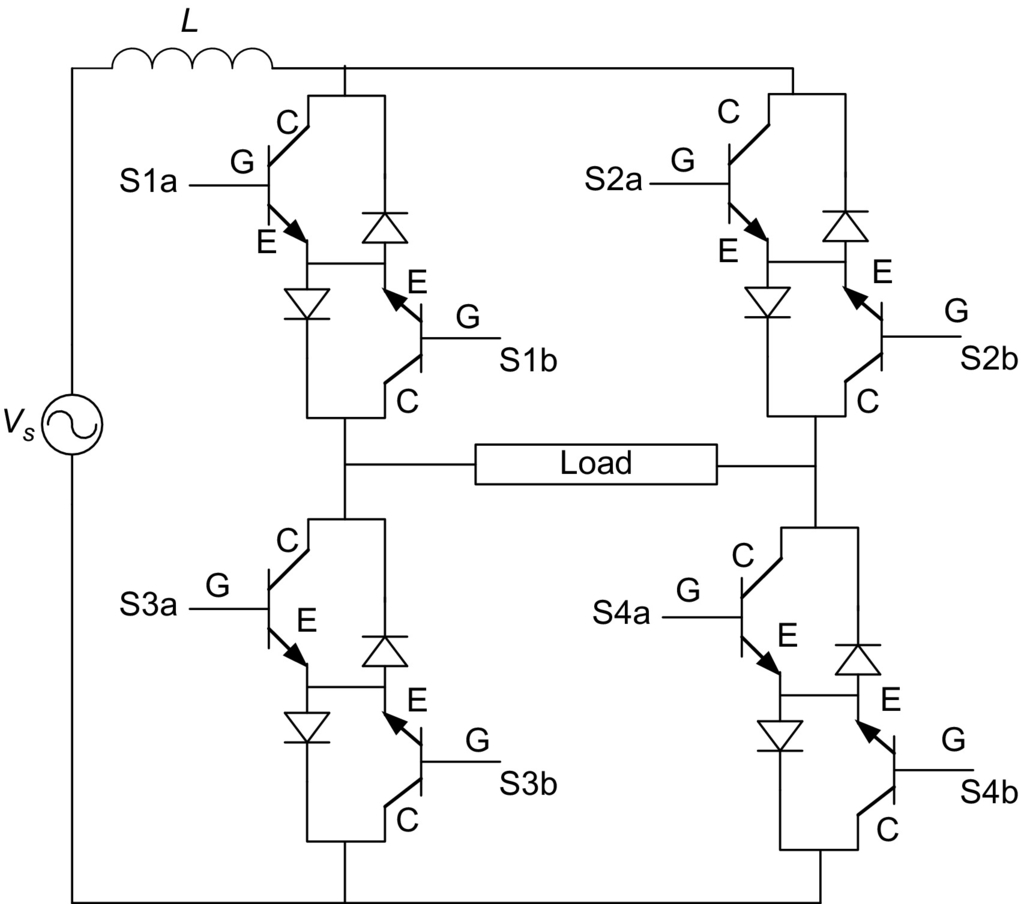
8.3.8 Controlled Rectifier Using Single Phase Matrix Converter (SPMC)—Boost Rectifier Operation
The commutation problem is the use of inductive loads where the commutation occurs during the pair of switches turn “off” making the energy in the inductor, being converted into switching spikes. Theoretically, the switching in the SPMC must be instantaneous and simultaneous; unfortunately, it is impossible for realization in practical systems due to turn-on/turn-off IGBT characteristics; to solve these difficulties, safe commutation strategy was developed in Ref. [18] to suppress the spikes induced by manipulation of the switch according to the switching pattern as in Fig. 2.
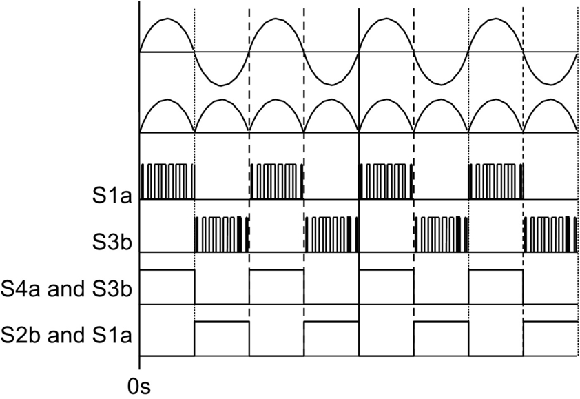
The controlled rectifier using SPMC for boost operation is shown in Fig. 8.44. A boost inductor L is connected at the ac side to reduce electromagnetic interference. The circuit in Fig. 8.44 operates in two modes; in the mode 1, S1a and S3a are switched “on” at t=0. And the input current flows through inductor L. At t=1, switches S1a and S4a are switched “on” at t=1, while S3a is switched “off.” Current would reverse and now flow through the load. The inductor current falls until switch S3a is turned “on” again in the next cycle. The energy stored in inductor L is then transferred to the load. The switching waveform is shown in the Fig. 8.45.