
5.4.5 GaN HEMT
5.4.5.1 GaN HEMT Structure
A GaN HEMT is a field-effect transistor in which two layers of different bandgaps and polarizations (GaN and AlGaN) are grown upon one another forming a heterojunction. As a consequence, in the vicinity of the heterojunction, positive charge is induced at the interface due to both spontaneous and piezoelectric type of polarization. Free electrons are transferred from the AlGaN layer, having higher conduction band energy, to the GaN layer, where the conduction band energy is lower, thus occupying a lower energy state and compensating for the induced positive charge [178]. The number of electrons is larger, especially if AlGaN is doped with impurities. Accumulated electrons along the heterojunction in a quantum well are usually referred to as two-dimensional electron gas (2DEG). The 2DEG is located in the channel of the HEMT, where current flows between the drain and the source controlled by the gate.
A cross section of a conventional GaN HEMT is shown in Fig. 5.32. HEMTs have been successfully grown on Si [179], sapphire [180], SiC [181], and GaN [182] substrates. SiC and sapphire substrates were the first used for HEMTs because of the existing experience in the light-emitting diode (LED) industry. However, successful growth of GaN HEMTs on Si substrates with parameters similar to HEMTs on SiC substrate has been reported lately. This is attractive to industry since Si substrates are available in large sizes and at low cost. Since SiC has three times the thermal conductivity of Si, HEMT transistors for low-power applications can be built on Si substrates, while for high-power applications, SiC substrates are preferred. The epitaxial layer grown on GaN substrates will not have a mismatch problem, but these substrates are extremely costly and small in size.
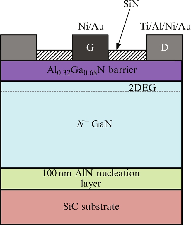
For HEMTs grown on foreign substrates, an intermediate, nucleation, or buffer layer is essential to the growth of quality GaN on the substrate. The morphology and crystal quality of a buffer layer play a critical role in determining the quality of epitaxial growth [183]. Aluminum nitride can be used as a nucleation layer. Metal-organic chemical vapor deposition and metal-organic molecular beam epitaxy methods can be used to form the AlN buffer layer. In [184], it is shown that there is no distinct difference between the GaN grown on a buffer layer obtained by the two methods.
The GaN epilayer grown on the top of the buffer layer is known as a channel layer because a channel is formed within. The channel layer is grown mostly by metal-organic chemical vapor deposition along the [0001] direction to benefit from the spontaneous polarization within the GaN wurtzite crystal. The temperature for growing the GaN epilayer is also important to the quality of the layer. As the temperature increases, the defect density and surface roughness decreases, which may be attributed to the improvement in the surface mobility and activities of source spaces on the substrate [184].
On the top of the channel layer, a barrier layer with a higher bandgap and lower electron affinity, compared with the GaN channel layer, is grown. The buffer layer can be fabricated with a group-III nitride material, such as AlxGayIn1−x−yN, where 0≦x≦1, 0≦y≦1 and x+y≦1 [185]. The thickness of the AlGaN barrier layer and the aluminum composition can be optimized so that a significant carrier concentration is induced and a 2DEG can be formed.
A passivation layer is deposited on the top of the barrier layer between the gate and the source and the second passivation layer between the drain and the gate. The layers may be initially formed as a single layer that is subsequently etched through to form the gate [185]. Different dielectric materials can be used, such as SiN, SiO2, Si, Ge, MgOx, MgNx, ZnO, SiNX, and SiOx, but usually, SiN is used. The deposition temperature and postannealing temperature of the passivation layer are important for controlling dynamic ON-state resistance degradation. The results given in [186] indicate that the SiN/AlGaN interface trap density is reduced by increasing the deposition temperature and also by increasing the postannealing temperature. Therefore, the current collapse in terms of dynamic ON-state resistance is also reduced.
As illustrated in Fig. 5.32, a conventional AlGaN/GaN HEMT has typically been fabricated with coplanar metal contacts. The source and drain electrodes are ohmic contacts providing low resistance and nonrectifying behavior, while the gate contact is intended to be a nonohmic Schottky barrier contact that controls the carrier concentration in the channel and blocks the current at large reverse voltages. Since the Schottky gate electrode and the 2DEG are separated by the AlGaN layer, the gate leakage current should be suppressed, but a relatively large gate leakage current is usually observed in the devices due to the defects near or at the surface of the AlGaN layer. The defects are formed during the epitaxial layer growth and by interface reaction between the metal and AlGaN layers interacting due to thermal treatments during the fabrication processes. Different materials have been used to create Schottky gate electrodes: Ni, Cu, Pt, and W. Pure metals have poor thermal stability on the AlGaN layer, while using electrodes with compound nitrides, such as TiN, the gate leakage current and the current collapse are suppressed to some extent. A characterization and comparison of poly-Si and TiN gate electrodes have shown advantages in reducing the leakage current and robustness against reverse-bias stressing of the poly-Si gate electrode [187].
Forming all three contacts on the same epitaxial layer may result in compromises between these characteristics. Therefore, there is a trade-off in device design, when selecting the doping and composition of the AlGaN barrier layer, between optimizing the source and drain ohmic contacts while optimizing the nonohmic gate contact [185]. Furthermore, high-power HEMTs should be optimized to provide as much current-carrying capability as possible to the region under the gate electrode while allowing the gate to block as high voltage as possible. Hence, it may be useful to have differences in the regions between the source and gate, under the gate, and between the gate and drain in order to modify the amount of energy band bending. Modifying the band bending will change the amount of the sheet region charge and the electric field profile within the device.
To improve electric performance together with reliability, new advanced structures have been designed and characterized. Introducing a field plate between the gate and drain electrodes enables electric field modulation. As a result, the electric field profile is reshaped, and the electric field is spread along the device's channel. Under the field plate, a depletion zone is formed so that the maximum peak value of the electric field at the drain side of the gate edge is reduced. Therefore, using a field-plate structure increases the device breakdown voltage, since the maximum electric field is distributed across the region among the gate and drain [188].
The phenomenon known as current collapse is associated with surface states in GaN-based HEMTs. It is caused by electrons trapped by defects in the GaN layer and the interface between the passivation film and the AlGaN barrier layer. Since, the electric field at the gate edge has a maximum value, it strongly affects the current collapse due to the acceleration of the electrons in the channel. The ON-resistance increase caused by the current collapse phenomena strongly depends on the gate-edge electric field. The results given in [189] show that the ON-state resistance increase caused by the current collapse phenomena is dramatically reduced by a field plate since the gate-edge electric field is reduced by the field-plate electrode.
The electron mobility in the 2DEG of an AlGaN/GaN heterostructure is an important transport parameter that characterizes the quality of the structure and determines the HEMT performance [190]. The 2DEG mobility is limited by a combination of various scattering mechanisms such as background impurities, polarization effects, degeneracy, interface roughness scattering, dislocations, scattering by acoustic and optical phonons, remote modulation doping scattering, and alloy disorder [191] and [192].
The electron mobility in the 2DEG is a function of the sheet electron density, NS, at the heterointerface over a wide temperature range. It increases with an increase in the sheet electron density, Ns, up to a maximum value and decreases with further increases in the density, NS. At a high sheet electron density in AlGaN/GaN heterostructures, the electrons spill from the quantum well near the heterointerface and occupy the delocalized states in the channel, leading to a reduction of the electron mobility. In this case, less effective screening and more pronounced ionized impurity scattering were observed when electrons occupied a much wider doped region near the heterointerface [193].
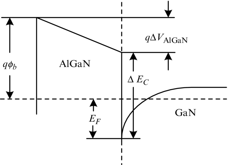
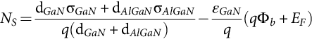
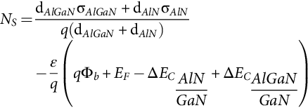
The sheet electron density near the AlGaN/GaN heterointerface is mainly contributed by the electrons induced by the doped AlGaN barrier and from the electrons generated by the piezoelectric effect. The sheet density of 2DEG is expressed as [194]:

where σAlGaN is the sheet charge density that is induced by AlGaN polarization, q is the electron charge, and ɛAlGaN and dAlGaN are the dielectric constant and the thickness of the AlGaN barrier. The potential drop, ΔVAlGaN, can be calculated as
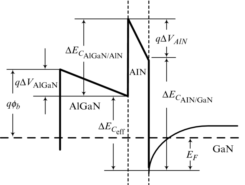
where Φb is the surface barrier height, EF is the Fermi level position with respect to the GaN conduction band edge at the AlGaN/GaN interface, and ΔEC is the conduction band discontinuity between GaN and AlGaN, as shown in Fig. 5.33.
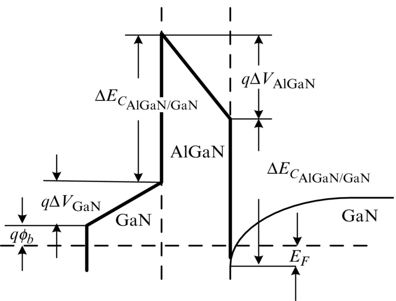
To decrease the sheet electron density, Ns, and improve the performance of the HEMT, a GaN capping layer placed between the barrier layer of AlGaN and the passivation layer of SiN is deposited as shown in Fig. 5.34. Strong polarization-induced electric fields are present in the AlGaN buffer layer and in the GaN capping layer that affect the 2DEC sheet density, depending on the thickness of the GaN capping layer. Experimental results given in [195] and the simulation results given in [196] show that the presence of a GaN capping layer results in a monotonic decrease of the sheet electron density with increases in the capping layer thickness. Decreasing the 2DEG sheet density results in modification of the electron scattering mechanisms and, therefore, modification in the mobility too. The experimental and simulation results show that as the thickness of the GaN capping layer increases, the electron mobility increases monotonically to a maximum point, where further increases in the capping layer thickness will cause the mobility to decrease slightly and eventually saturate [195] and [196].

The 2DEG sheet resistance of the GaN/AlGaN/GaN structure can be calculated by the following equation [194]:
where σGaN is the sheet charge density that is induced by the GaN polarization and ɛGaN and dGaN are dielectric constant and the thickness of the GaN capping layer, respectively. The surface barrier height, Φb, and the Fermi level position, EF, are shown in Fig. 5.35.
To achieve better HEMT performance, a thin AlN (∼1 nm) interlayer at the AlGaN/GaN interface is added in some advanced structures. The insertion of the thin AlN interlayer suppresses the penetration of the wave function into the barrier and effectively removes alloy scattering and pushes out most of the 2DEG from the barrier. The small finite part that still penetrates the barrier is not affected by the allow scattering [197]. Also, additional polarization due to the AlN interlayer is observed. As a result, the sheet charge density and mobility are improved as compared with the conventional AlGaN/GaN heterostructure having equivalent AlGaN parameters.
At small drain bias, VDS, the conductivity between the source and drain, known as 2DEG conductivity, is proportional to the product of channel mobility, μ, and the sheet electron density, NS:
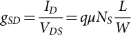
where ID is the drain current and L and W are the length and width of the gate. Therefore, insertion of an AlN layer increases the conductivity. In [198], it is reported that introduction of an AlN interlayer improved the ON-state resistance and current, RON and ION, by 10%.
The 2DEG sheet resistance of GaN/AlN/AlGaN structure can be calculated by the following equation according to [194]:
where σAlN is the sheet charge density that is induced by AlN polarization and ɛAlN and dAlN are the dielectric constant and thickness of the AlN capping layer, respectively. The surface barrier height, Φb, and the Fermi level position, EF, of the GaN/AlN/AlGaN structure are shown in Fig. 5.36.
A critical requirement of the power switch is that it has low ON-resistance, RON, immediately after switching from OFF-state to ON-state. The ON-resistance, RON, of a HEMT is expressed by the following equation:
where RC is the source and drain contact resistance, RS, is the parasitic source resistance, RD, is the parasitic drain resistance, and RCH is the channel resistance. The carrier trapping at the surface and the buffer traps degrade the device performance. In a GaN HEMT, the parasitic charge moving in and out of the traps affects the density of the 2DEG and causes ON-resistance degradation. To characterize the dynamic ON-resistance of a HEMT, a switching test should be performed using Fig. 5.37. The gate source of the device is connected to a pulsed generator that can switch the device from OFF- to ON-state. During the OFF-state, high-voltage VDD is applied to the device. The load resistance, RL, is connected in series with the device under test, and it is adjusted so that the ON-state resistance is measured in the linear region. The turn-ON and turn-OFF time are fixed during the experiment. Turn-OFF time should be long enough, typically larger than 10 ms, so the device under test cools down and its temperature does not affect the results. The ON-time is larger than the time at which the dynamic resistance is measured or the time at which the drain current, ID, saturates.

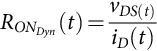
The transient drain current through the device, iD(t), and the drain-source voltage, vDS(t), are recorded, and the resistance is calculated for different times by the equation:
The static ON-resistance, RONstatic, is calculated by the same equation; only the saturated values for the current and the voltage are used. The experiment and calculation can be repeated for different values of the load resistance (i.e., different drain current). In Fig. 5.38A is a sketch of the gate-source voltage applied to the device under test, the drain-source voltage and the drain current. While in Fig. 5.38B showed a sketch of the dependency of drain current ID, as a function of drain-source voltage, VDS, for times t1 and t2 and different values of the load resistance.
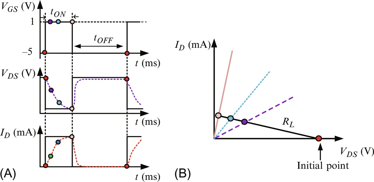
The current collapse can be defined as a normalized dynamic ON-resistance (i.e., a ratio of the dynamic resistance value to its static value). The ratio can be used to compare the performances of HEMTs.
5.4.5.2 GaN HEMT DC Characteristics
The current-voltage characteristics of a HEMT are related to the density variation of the 2DEG where 2DEG depends on the gate-source voltage, VGS, applied to the HEMT. Moreover, any changes of VGS have an effect on the electron mobility in the channel. A HEMT has three modes of operation: linear, saturation, and cut-OFF. For power applications and the linear mode of operation, the low-field mobility of the electrons in 2DEG, μn, is used to calculate the drain current, while when the drain-source voltage increases, the mobility of the electrons in the 2DEG decreases. In this case, a simple model for high field mobility, μnHV, based on the geometry of the HEMT structure is used:
where LCH is the channel length and vsat is the saturation velocity. The drain current, iD, is proportional to the density of electrons in the channel [199]:

where W is the channel width. The drain current can be obtained by integrating the current along the channel. If the source and drain contact resistances are neglected and the boundary conditions are used,
then the drain current in the linear regime of operation is

where CGS is the gate-to-source capacitance and Vth is the threshold voltage. In the saturation regime of operation, the drain current is
5.4.5.3 GaN HEMT Design Considerations
To improve the performance and also protect GaN HEMTs from damage, the designer should take into account some very important concerns and benefits.
The threshold voltages of GaN HEMTs are low compared with the Si and SiC MOSFETs. Some of the HEMT devices start to conduct current at significantly low gate-source voltage (1.4 V) that makes it difficult to ensure that the device turns OFF, especially at low temperatures (the threshold voltage decreases as the temperature drops). Negative voltage should be used in this case to ensure turn-OFF of the device. This behavior indicates that the threshold voltage has a positive temperature coefficient. HEMTs are unipolar devices (i.e., no minority carriers are involved during conduction). Therefore, there is no reverse recovery charge and thus very small reverse recovery losses.
As it can be seen in Figs. 5.32 and 5.34, GaN HEMTs do not have an intrinsic body diode as in Si and SiC MOSFETs. However, they have a so-called “body-diode” effect that makes the device conduct under applied reverse voltages. The mechanism for an enhancement GaN HEMT to behave as a diode during turn-OFF is as follows [200]. When the gate-source voltage is zero and the drain-source voltage is positive, no channel is created, and therefore, current is not flowing. As the drain-source voltage starts to become negative, a positive bias on the gate relative to the drift region is formed, injecting electrons under the gate. The gate-to-drain voltage starts to increase, and when it reaches the threshold voltage, there will be a significant amount of electrons under the gate to form a conduction channel.
The temperature coefficient of the ON-state resistance, RON, of a GaN HEMT is positive, similar to Si and SiC MOSFETs, but the magnitude is small compared with a Si MOSFET and approximately in the same range as a SiC MOSFET.
Since GaN HEMTs have high switching speed, the voltage slew rate may be more than ten to hundreds of volts per nanosecond, and the current slew rate may be more than 10 A s−1. Such a high slew rate may lead to the so-called Miller effect (i.e., undesirable or parasitic turn-ON of the power transistor and that creates a short circuit that will cause significant damage resulting in destruction of the HEMT).
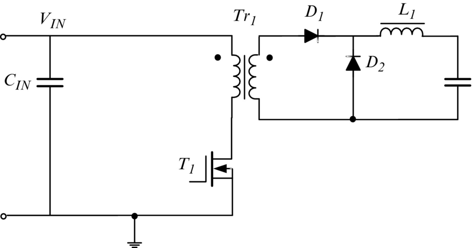
Shown in Fig. 5.39A is a synchronous buck converter. If the upper HEMT is switched ON, the lower one has to be OFF in order to avoid a shoot-through condition and, therefore, possible failure of the HEMT due to overcurrent.

The mechanism of the parasitic switching for the synchronous buck can be explained with the capacitive voltage divider formed between the gate to drain and gate to source of the low-side transistor (Fig. 5.39B). The gate-source voltage of the low-side transistor is
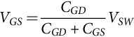
where CGD and CGS are the gate-drain and gate-source capacitances, respectively, and VSW is the switching node voltage. Although the gate of the low HEMT is set to zero by the driver circuit, there is a possibility that the low-side HEMT turns ON because of the fast change in the switching voltage. The rate of change of the voltage at the switching node, VSW, is approximately Vin/tr, where Vin is the converter input voltage and tr is the rise time. The voltage slew causes a current to flow through gate-to-drain capacitance of the low-side HEMT:
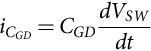
This current flows into the equivalent impedance of driver pull-down resistance in series with the gate resistance and both of them in parallel to the gate-source capacitance of the low HEMT. If the gate-source voltage during the rise time of the high side transistor is higher than the threshold voltage, the low HEMT will turn ON parasitically. One way to prevent this from happening is to split the gate pull-up and pull-down connection in the driver and allowing for the insertion of discrete resistors, if needed. The low (OFF-state) pull-down resistance should be a lower resistance value than the pull-up resistance value. If the driver does not support a separate turn-OFF resistor, a diode in parallel can be used, as shown in Fig. 5.40.
The high slew rate may also cause ringing and, in some cases, damage if the common source inductance, LS, is not minimized. The source current, iS, is the sum of the drain and the gate currents. Any voltage induced on the common source inductance ![]() will show up as ringing in the gate-source voltage. To address this issue, one company developed packages with exceptionally low internal inductance by implementing source-sense or Kelvin connection, but the external inductance that contributes to the ringing should also be minimized. Shown in Fig. 5.41 is a Kelvin connection at the source of a HEMT where the ground return of the gate driver is connected directly to the source on the die internal to the package by a star-point connection. In this case, the external parasitic inductances and resistances in the gate loop will be minimized, and the high slew rate of the drain current during turn-ON switching cannot influence the gate current loop.
will show up as ringing in the gate-source voltage. To address this issue, one company developed packages with exceptionally low internal inductance by implementing source-sense or Kelvin connection, but the external inductance that contributes to the ringing should also be minimized. Shown in Fig. 5.41 is a Kelvin connection at the source of a HEMT where the ground return of the gate driver is connected directly to the source on the die internal to the package by a star-point connection. In this case, the external parasitic inductances and resistances in the gate loop will be minimized, and the high slew rate of the drain current during turn-ON switching cannot influence the gate current loop.

However, the (PCB) layout should be carefully considered to minimize the effect of the parasitic inductance. For this purpose, the designers should keep the connection from the output of the driver to the HEMT gate and from the Kelvin connection to the gate return path of the driver as short as possible. To reduce the wire parasitic inductance, the two paths should be on separate board layers physically over each other. In this case, the magnetic flux generated by two current flows will cancel each other and will lower the parasitic inductance. Also, the connection for the decoupling capacitor of the driver power supply should be short.
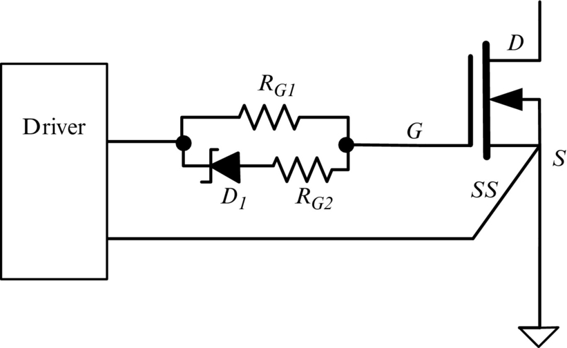
During the fast switching transition, the Miller capacitance combined with parasitic inductance in the gate-source loop may induce over- or undershoot voltage spikes that could possibly exceed the maximum gate-source voltage rating of the device. This can be avoided by optimizing the PCB layout, but if the spikes still remain after overvoltage clamping a Zener diode and a capacitor in parallel is included as it shown in Fig. 5.42A can be used [201]. If a negative gate-source voltage is used to turn OFF the HEMT, the overvoltage clamp will have two Zener diodes connected back to back as shown in Fig. 5.42B. For effective clamping, the diode and the capacitor should be placed as close to the device gate as possible.
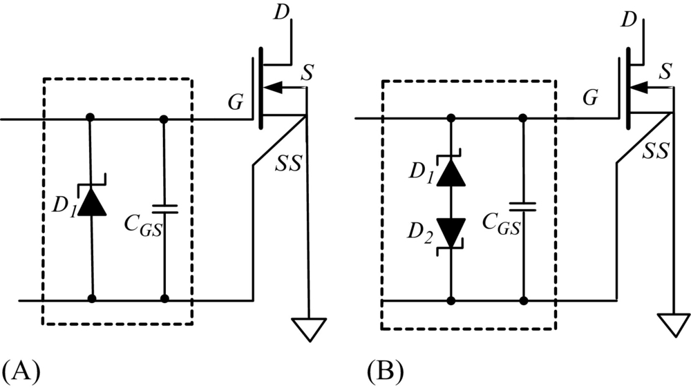
To enable high switching, high power density, and low system cost, some companies are fabricating a gate drive and logic circuit with GaN power FETs on a single chip, as shown in Fig. 5.43. The advantages of this type of arrangement are that there is no gate-loop parasitic inductance and, therefore, the output signal will be absent of ringing; has a fast rise-time gate signal; and the ability to have rail-to-rail gate signal values. Plus, it offers high-frequency operation with minimal propagation delay [202].
Unlike many conventional Si MOSFETs, the GaN HEMTs are not avalanche rated at the breakdown at the drain-source junction. Therefore, in order to maintain reliability, the maximum drain-source voltage, VDS, should be guaranteed by design. For some topologies, Si MOSFETs can be directly substituted for GaN HEMTs with the same breakdown voltage. An example of this type of topology is a full bridge converter controlled as a dual synchronous buck, as shown in Fig. 5.44 [203].

While for some resonance topologies, Si MOSFETs cannot be replaced with GaN HEMTs that have the same breakdown voltage. Shown in Fig. 5.45 is a resonant-reset forward converter.
After the switch turns OFF, the magnetizing current reverses in a sinusoidal fashion set by the magnetizing inductance, Lm, and the resonance capacitance, CR. The resonance capacitance, CR, is a sum of all capacitances across the primary winding of the transformer including the reflected diode capacitance, CD:

where CDS is the switch drain-source capacitance, CT is transformer primary windings capacitance, and NS/NP is the transformer winding ratio. The drain-source capacitance, CDS, is dominant in this expression. The drain-source peak voltage, VDSpeak, of the switch depends on the characteristic impedance ![]() and can be calculated by the equation:
and can be calculated by the equation:

where the peak primary current is
From the last three equations, it can be concluded that if only switches are different in the circuit shown in Fig. 5.45, the maximum drain-to-source voltage that will be applied to the switch depends on the drain-source capacitance, CDS. Since GaN HEMTs have significantly smaller capacitance, the peak voltage, VP, will be significantly larger, and therefore, the peak drain-source voltage will correspondingly be larger. In order to maintain maximum reliability, GaN HEMTs should be rated for higher voltages than the Si MOSFETs in any particular application.
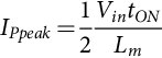
Although GaN high-power HEMTs have significantly low switching and conduction power losses, compared with MOSFETs in Si or SiC, during high-power and high-frequency operation, their temperature is increased. Thermal management is another very important consideration for designers. The current fabrication methodology of HEMT structures implies that the gate, drain, and source connections must be made on the same side of the die. For this reason, necessary isolation gaps must be included between these contacts as this mounting technique results in a higher thermal resistance. To improve the thermal resistance, the package of HEMTs has a thermal pad on the bottom side that is connected to the substrate through high-density microvias with copper providing the low thermal resistance path. To optimize the device performance, the thermal pad must always be connected to the source. For most effective cooling, a heat sink can be attached to the PCB bottom copper pad with the recommended thermally conductive interface pad or film between the heat sink and the bottom copper pad. Also, the top copper layer should be a 2 oz or thicker layer. A PCB with four or more internal layers is desirable. To improve the heat transfer is to add plated, through-hole thermal vias between conductive layers, but no vias should be placed under the solder bars unless they are microvias and completely filled with copper [200]. Vias with holes located directly under the gate, source, or drain solder bars will reduce the transistor's temperature cycling performance. In Fig. 5.46, a cross-sectional view of the GaN HEMT package and thermal dissipation path through the PCB, vias, and the heat sink is shown [204].
Appendix Lightly Doped Drift Region Thickness
One of the requirements for choosing a proper power electronic device for a converter is that it must possess a low specific ON-resistance. The specific ON-resistance of a bipolar device is related to the width and doping concentration of the lightly doped drift region (N− base). This means that the doping concentration and the width of the low-doped base region in a bipolar device must be carefully considered to achieve a desired avalanche breakdown voltage and ON-resistance (conduction characteristics).
The avalanche breakdown voltage, VBD, for an abrupt parallel plate junction, is a function of the background doping and the semiconductor properties, such as dielectric constant, energy bandgap, and impact ionization coefficient. Breakdown occurs when the carrier multiplication becomes greater than unity. Impact ionization coefficients empirically describe the exponential relationship of the applied electric field and associated charge-carrier creation. The impact ionization coefficients for electrons and holes have different values, and values for semiconductor materials of interest are obtained empirically. The general ionization coefficient has been determined to have a theoretical form that is exponential and represented by [205]:
where ![]() is the electric field (V cm−1), Ai is the amplitude parameter (cm−1), bi is the ionization energy parameter related to the mean free path between collisions (V cm−1), and mi is an additional fit parameter for use with a multitude of semiconductor materials [205,206]. These parameter values depend on the semiconductor material, and they are different for electrons or holes. For Si, 6H-SiC, and GaN, mi has been determined to be 1 for both electrons and holes [205,206].
is the electric field (V cm−1), Ai is the amplitude parameter (cm−1), bi is the ionization energy parameter related to the mean free path between collisions (V cm−1), and mi is an additional fit parameter for use with a multitude of semiconductor materials [205,206]. These parameter values depend on the semiconductor material, and they are different for electrons or holes. For Si, 6H-SiC, and GaN, mi has been determined to be 1 for both electrons and holes [205,206].
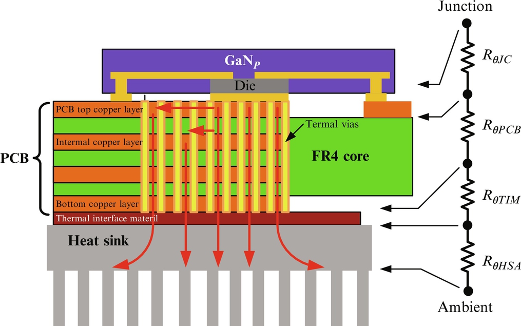
Near the breakdown condition, a small error is introduced by equating the impact ionization coefficients of electrons and holes to an effective ionization coefficient, αeff. In this case, the breakdown voltage is defined as the applied voltage at which the summed effects described by the ionization coefficient acting over the depletion width, W, create more free charge carriers. The boundary at breakdown is when the integral Eq. (A.2) achieves a value of unity [207]. The associated breakdown condition in terms of the effective ionization coefficient is:
Evaluation of this integral using Eq. (A.1) is very difficult; and no analytical expressions result, thus limiting its usefulness for device design. However, a simplified (and purely empirical) polynomial expression for the ionization coefficient in terms of the electric field is widely used [207]:
The two previous fit parameters, Ai and bi, are absorbed into the prefactor, K. The coefficient, K, is expressed in terms of new parameters, A, b, and m, that are averages of the previous Ai, bi, and mi values, expressed in Eq. (A.1) for holes and electrons [206]:
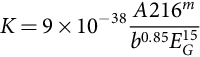
where EG is the bandgap energy (eV) for the semiconductor material of interest.
For a one-sided abrupt P+-N junction, the electric field and the voltage across the lightly doped region are functions of the depletion distance and depend on the impurity doping concentration, ND1, in the lightly doped N-base and the depleted N-base width, W. The electric field and voltage relations are presented in Eqs. (A.5), (A.6), respectively.
The maximum electric field is observed at junction (x=0). Using this and substituting Eq. (A.5) in Eq. (A.3) and then substituting into the integral Eq. (A.2), one can obtain the minimum width of the depletion layer, Wmin, at breakdown [206].

The corresponding breakdown voltage can then be determined from Eq. (A.6) as
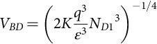
It should be noted that the permittivity is correctly placed in the denominator in Eq. (A.8), not in the numerator as was presented in the expressions from [206].
To reduce the lightly doped region width and maintain the same breakdown voltage requires the addition of a highly doped N+ buffer layer at the end of the drift (N-base) region to create a P+N–N+ structure. This will modify the expressions for the minimum width of the depletion layer, Wmin, and the corresponding breakdown voltage, VBD. Reducing the width of the base region will decrease the effective on-resistance during conduction and reduce the volume of stored charge, thus decreasing the turn-OFF (and turn-ON) time.
To reduce the thickness of the drift region for the same blocking voltage, a heavily doped N+-type buffer layer should be added to the end of the drift region to create a P+N–N+ structure Fig. A.1B. Due to the high doping level in the buffer layer, the gradient of the electric field will be steep and positive, in the same way as in the P-type region. The electric field has maximum value at the P+N− junction. The electric field in the drift region will decrease gradually with no requirement for an excessive depletion layer width. The phenomenon that occurs when the depletion layer extends across the entire drift region is known as punch-through.
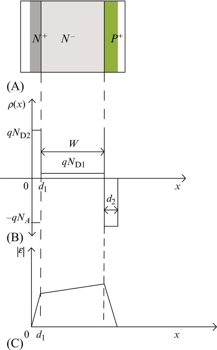
Consider a two-dimensional P+N−N+ structure under equilibrium conditions with the doping profile sketched in Fig. A.1. The electric field in the different regions can be obtained by substituting the charge densities into Poisson's equations and then integrating:
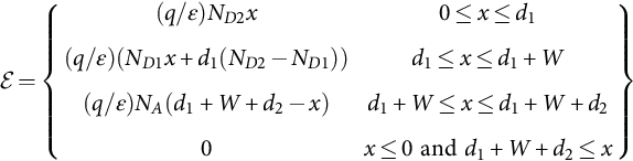
where the respective impurity doping concentrations for the N+N−P+ regions are ND2, ND1, and NA. The corresponding depletion region thicknesses of each section are d1, W, and d2.
The maximum electric field of the P+N−N+ structure will be at the N−P+ junction ![]() . Charge neutrality from Eq. (A.9) gives the depletion thickness, d2 of the P+ region as
. Charge neutrality from Eq. (A.9) gives the depletion thickness, d2 of the P+ region as
Since ![]() , the electric potential applied to the structure is obtained by integrating the electric field from 0 to
, the electric potential applied to the structure is obtained by integrating the electric field from 0 to ![]() resulting in
resulting in

Substituting Eqs. (A.11) into (A.10) and using the result to calculate the ionization coefficient Eq. (A.3), we can reevaluate the ionization integral Eq. (A.2) as
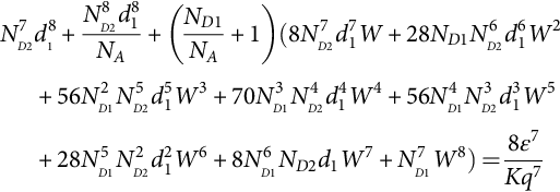
For a given breakdown voltage, BV, the thicknesses of the drift region, W, can be calculated numerically using Eqs. (A.11), (A.12).