
11.4.4 Space-Vector-Based Modulating Techniques in CSIs
The objective of the SV-based modulating technique is to generate PWM load line currents that are on average equal to given load line currents. This is done digitally in each sampling period by properly selecting the switch states from the valid ones of the CSI (Table 11.6) and the proper calculation of the period of times they are used. As in VSIs, the selection and time calculations are based upon the space-vector transformation.
11.4.4.1 Space-Vector Transformation in CSIs
Similarly to VSIs, the vector of three-phase line-modulating signals iabcc=[icaicbicc]T![]() can be represented by the complex vector →ic=iαβc=[icαicβ]T
can be represented by the complex vector →ic=iαβc=[icαicβ]T![]() by means of Eqs. (11.31) and (11.32). For three-phase balanced sinusoidal modulating waveforms, which feature an amplitude îc and an angular frequency ω, the resulting modulating signal complex vector →ic=iαβc
by means of Eqs. (11.31) and (11.32). For three-phase balanced sinusoidal modulating waveforms, which feature an amplitude îc and an angular frequency ω, the resulting modulating signal complex vector →ic=iαβc![]() becomes a vector of fixed module îc, which rotates at frequency ω (Fig. 11.37). Similarly, the SV transformation is applied to the line currents of the nine states of the CSI normalized with respect to ii, which generates nine space vectors (→ii
becomes a vector of fixed module îc, which rotates at frequency ω (Fig. 11.37). Similarly, the SV transformation is applied to the line currents of the nine states of the CSI normalized with respect to ii, which generates nine space vectors (→ii![]() , i=1,2,…,9
, i=1,2,…,9![]() in Fig. 11.37). As expected, →i1
in Fig. 11.37). As expected, →i1![]() to →i6
to →i6![]() are nonnull line current vectors, and →i7
are nonnull line current vectors, and →i7![]() , →i8
, →i8![]() , and →i9
, and →i9![]() are null line current vectors.
are null line current vectors.
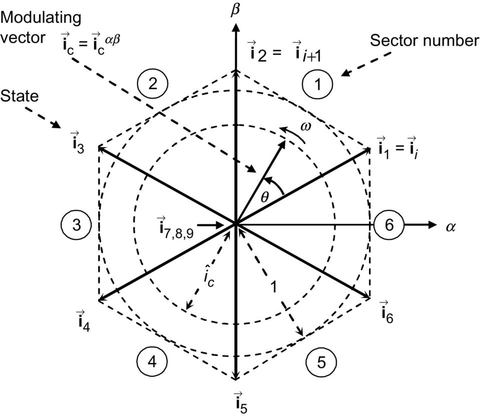
The SV technique approximates the line-modulating signal space vector →ic![]() by using the nine space vectors (→ii
by using the nine space vectors (→ii![]() , i=1,2,…,9
, i=1,2,…,9![]() ) available in CSIs. If the modulating signal vector →ic
) available in CSIs. If the modulating signal vector →ic![]() is between the arbitrary vectors →ii
is between the arbitrary vectors →ii![]() and →ii+1
and →ii+1![]() , then →ii
, then →ii![]() and →ii+1
and →ii+1![]() combined with one zero SV (→iz=→i7
combined with one zero SV (→iz=→i7![]() or →i8
or →i8![]() or →i9
or →i9![]() ) should be used to generate →ic
) should be used to generate →ic![]() . To ensure that the generated current in one sampling period Ts (made up of the currents provided by the vectors →ii
. To ensure that the generated current in one sampling period Ts (made up of the currents provided by the vectors →ii![]() , →ii+1
, →ii+1![]() , and →iz
, and →iz![]() used during times Ti, Ti+1
used during times Ti, Ti+1![]() , and Tz)
, and Tz)![]() is on average equal to the vector →ic
is on average equal to the vector →ic![]() , the following expressions should hold:
, the following expressions should hold:
Ti=Ts⋅ˆic⋅sin(π/3−θ)
Ti+1=Ts⋅ˆic⋅sin(θ)
Tz=Ts−Ti−Ti+1
where 0≤ˆic≤1![]() . Although the SVM technique selects the vectors to be used and their respective on-times, the sequence in which they are used, the selection of the zero space vector, and the normalized sampled frequency remain undetermined.
. Although the SVM technique selects the vectors to be used and their respective on-times, the sequence in which they are used, the selection of the zero space vector, and the normalized sampled frequency remain undetermined.
11.4.4.2 Space-Vector Sequences and Zero Space-Vector Selection
Although there is no systematic approach to generate a SV sequence, a graphic representation shows that the sequence →ii![]() , →iz
, →iz![]() , →ii+1
, →ii+1![]() (where the chosen →iz
(where the chosen →iz![]() depends upon the sector) provides high performance in terms of minimizing unwanted harmonics and reducing the switching frequency. To obtain the zero SV that minimizes the switching frequency, it is assumed that Ic is in sector ②. Then, Fig. 11.38 shows all the possible transitions that could be found in sector ②. It can be seen that the zero vector →i9
depends upon the sector) provides high performance in terms of minimizing unwanted harmonics and reducing the switching frequency. To obtain the zero SV that minimizes the switching frequency, it is assumed that Ic is in sector ②. Then, Fig. 11.38 shows all the possible transitions that could be found in sector ②. It can be seen that the zero vector →i9![]() should be chosen to minimize the switching frequency in all cases. Table 11.7 gives a summary of the zero space vector to be used in each sector in order to minimize the switching frequency. However, it should be noted that Table 11.7 is valid only for the sequence →ii
should be chosen to minimize the switching frequency in all cases. Table 11.7 gives a summary of the zero space vector to be used in each sector in order to minimize the switching frequency. However, it should be noted that Table 11.7 is valid only for the sequence →ii![]() , →ii+1
, →ii+1![]() , →iz
, →iz![]() . Another sequence will require reformulating the zero space-vector selection algorithm.
. Another sequence will require reformulating the zero space-vector selection algorithm.

 or →i2⇔→iz⇔→i1
 ; (B) transition, →i1⇔→iz⇔→i1
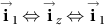 ; and (C) transition, →i2⇔→iz⇔→i2
 .
.
11.4.4.3 The Normalized Sampling Frequency
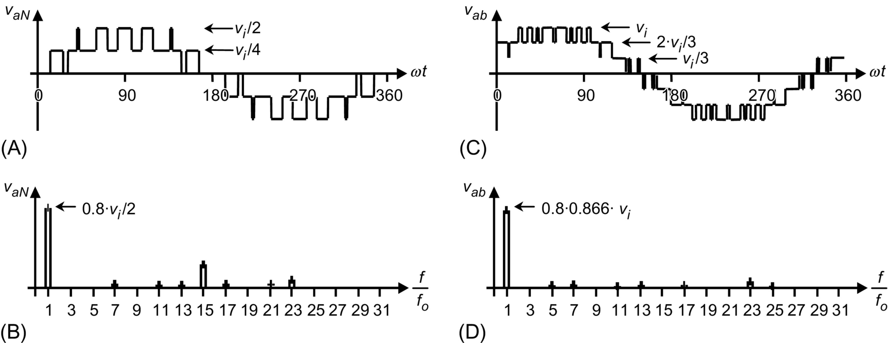
As in VSIs modulated by an SV approach, the normalized sampling frequency fsn should be an integer multiple of 6 to minimize uncharacteristic harmonics. As an example, Fig. 11.39 shows the relevant waveforms of a CSI SVM for fsn=18![]() and ˆic=0.8
and ˆic=0.8![]() . Fig. 11.39 also shows that the first set of relevant harmonics load line current are at fsn.
. Fig. 11.39 also shows that the first set of relevant harmonics load line current are at fsn.

 , fsn=18
 ): (A) modulating signals, (B) switch S1 state, (C) switch S3 state, (D) ac output current, (E) ac output current spectrum, (F) ac output voltage, (G) dc voltage, (H) dc voltage spectrum, (I) switch S1 current, and (J) switch S1 voltage.
11.4.5 DC Link Voltage in Three-phase CSIs
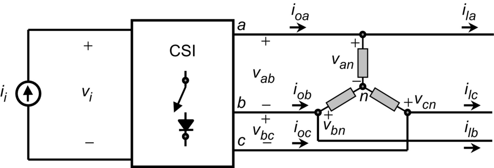
An instantaneous power balance indicates that
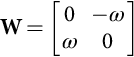
vi(t)⋅ii(t)=van(t)⋅ioa(t)+vbn(t)⋅iob(t)+vcn(t)⋅ioc(t)
where van(t), vbn(t), and vcn(t) are the phase filter voltages as shown in Fig. 11.40. If the filter is large enough and a relatively high switching frequency is used, the phase voltages become nearly sinusoidal balanced waveforms. On the other hand, if the ac output currents are considered sinusoidal and the dc link current is assumed constant ii(t)=Ii![]() , Eq. (11.55) can be simplified to
, Eq. (11.55) can be simplified to
vi(t)=1Ii{,√2Vonsin(ωt)⋅√2Io1sin(ωt−ϕ)+√2Vonsin(ωt−120∘)⋅√2Io1sin(ωt−120°−ϕ)+√2Vonsin(ωt−240∘)⋅√2Io1sin(ωt−240°−ϕ),}
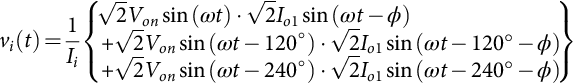
where Von is the rms ac output phase voltage, Io1 is the rms fundamental line current, and ϕ is an arbitrary filter-load angle. Hence, the dc link voltage expression can be further simplified to the following:
vi(t)=3Io1IiVoncos(ϕ)=√3Io1IiVocos(ϕ)
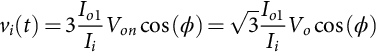
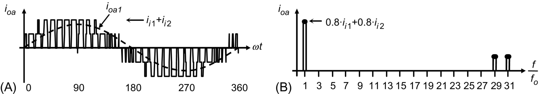
where Vo=√3Von![]() is the rms load line voltage. The resulting dc link voltage expression indicates that the first line current harmonic Io1 generates a clean dc current. However, as the load line currents contain harmonics around the normalized sampling frequency fsn, the dc link current will contain harmonics but around fsn as shown in Fig. 11.39H. Similarly, in carrier-based PWM techniques, the dc link current will contain harmonics around the carrier frequency mf (Fig. 11.31).
is the rms load line voltage. The resulting dc link voltage expression indicates that the first line current harmonic Io1 generates a clean dc current. However, as the load line currents contain harmonics around the normalized sampling frequency fsn, the dc link current will contain harmonics but around fsn as shown in Fig. 11.39H. Similarly, in carrier-based PWM techniques, the dc link current will contain harmonics around the carrier frequency mf (Fig. 11.31).
In practical implementations, a CSI requires a dc current source that should behave as a constant (as required by PWM CSIs) or variable (as square-wave CSIs) current source. Such current sources should be implemented as separate units.
11.5 Multilevel Inverters
The traditional inverters can generate an output in two or three different levels. For instance, a single-phase full-bridge inverter can produce vi, −vi![]() , and zero; this type of output is unacceptable in the medium- to high-voltage ranges due to the high dv/dt present in the PWM ac line voltages. In order to solve this, the multilevel inverters were initially proposed. However, now, their use has been more extended not only due to the low harmonic content obtained at low switching frequencies but also for the good efficiency obtained.
, and zero; this type of output is unacceptable in the medium- to high-voltage ranges due to the high dv/dt present in the PWM ac line voltages. In order to solve this, the multilevel inverters were initially proposed. However, now, their use has been more extended not only due to the low harmonic content obtained at low switching frequencies but also for the good efficiency obtained.
Different multilevel topologies have been proposed. The goal is to produce an output defined by different levels that can be voltage or current levels. The basic principle is to connect the output to multiple points, one at a time. Fig. 11.41A shows the idea for a voltage-source configuration. Usually, the number M of possible level defines the name of the inverter; for instance, if five points are available as in Fig. 11.41A (M=5), the inverter is usually named a five-level inverter.

For a five-level inverter, the output voltage shown in Fig. 11.41B would be produced. By simple inspection, this output voltage looks more similar to a sinusoidal waveform; then, the harmonic content is expected to be lower than traditional inverters, and the power semiconductors are operating at low switching frequency.
11.5.1 Voltage Source-Based Multilevel Topologies
The three-phase VSI can be called also two-level VSI due to the fact that the inverter phase voltages vaN, vbN, and vcN (Fig. 11.17) are instantaneously either vi/2 or − vi/2. In other words, the phase voltages can take one of the two voltage levels. However, regarding to multilevel inverters, the topologies usually have more than two levels.
The typical multilevel voltage-source topologies are the neutral-point-clamped (also called diode-clamped) inverters, the flying capacitors, and the cascaded configuration. Since they are voltage-source converters, the compulsory rules described in Section 11.2.1 also apply, but certainly, some remarks are made for each converter.
11.5.1.1 Neutral Point Clamped Inverter
In Fig. 11.42, the neutral-point-clamped inverter is shown (three levels). For this topology, not only an M-level inverter requires (M−1) capacitors and 2(M−1) switching semiconductors per leg, but also 2(M−2) additional diodes must be included per leg; for instance, Da+ and Da− are added for the left leg. M−1 devices per leg must be on to select the desired level.
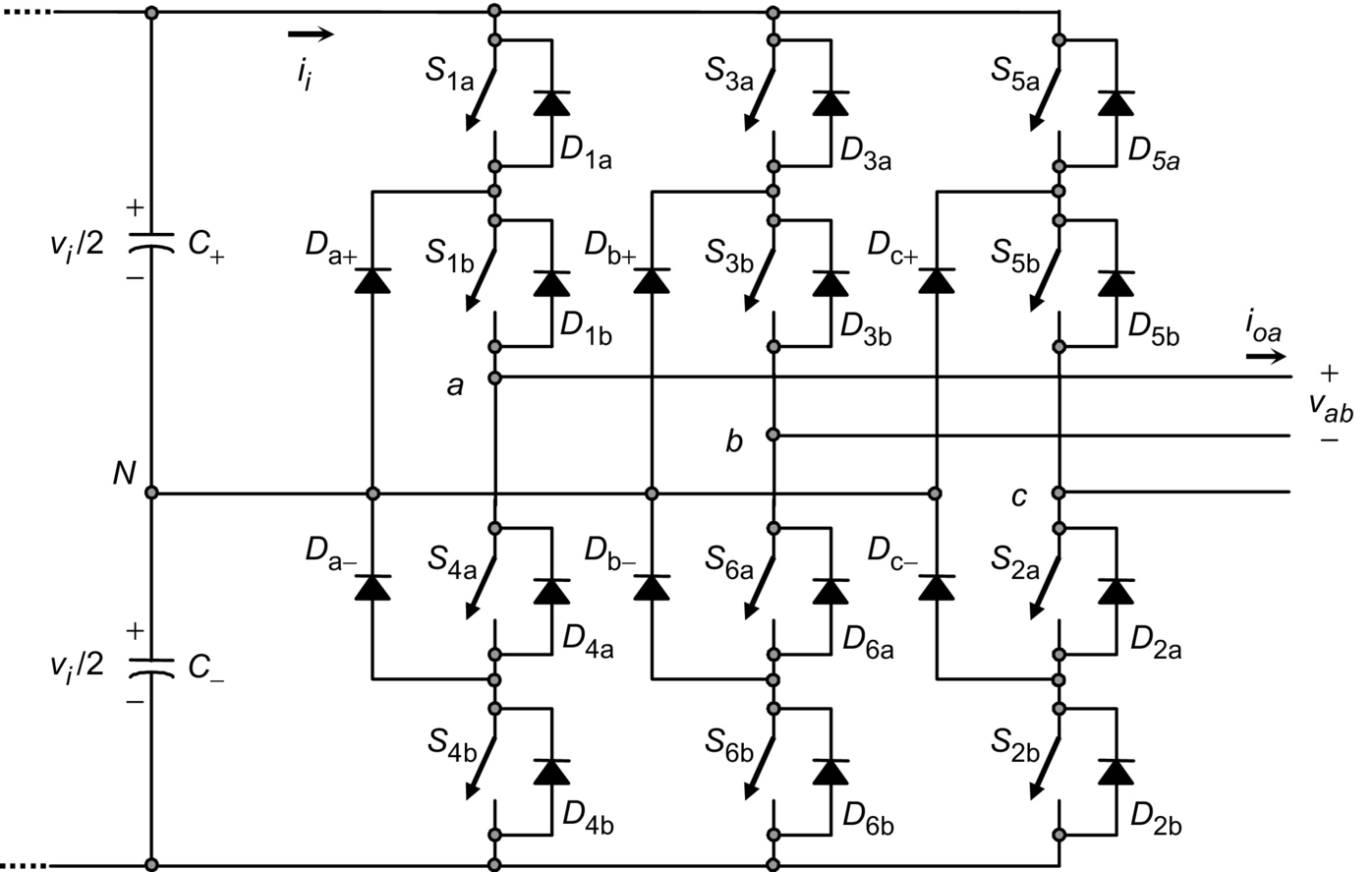
Table 11.8 gives the switch states of the three-level inverter, just left leg. As it can be observed, not only always two switches are on, but also the signal S1a is the opposite of S4a, and S1b is the opposite of S4b. These conditions must be always satisfied. The switch states for phases b and c are identical to those of phase a.

11.5.1.2 Flying Capacitors Inverter
In Fig. 11.43, the flying capacitor inverter is shown (three levels). For this topology, an M-level inverter requires ∑M−1j=1(M−j)![]() capacitors per leg (considering that the capacitors have the same voltage rating) and 2(M−1) switching semiconductors per leg, but no additional diodes are required. Also M−1 switches per leg must be on to select the desired level.
capacitors per leg (considering that the capacitors have the same voltage rating) and 2(M−1) switching semiconductors per leg, but no additional diodes are required. Also M−1 switches per leg must be on to select the desired level.
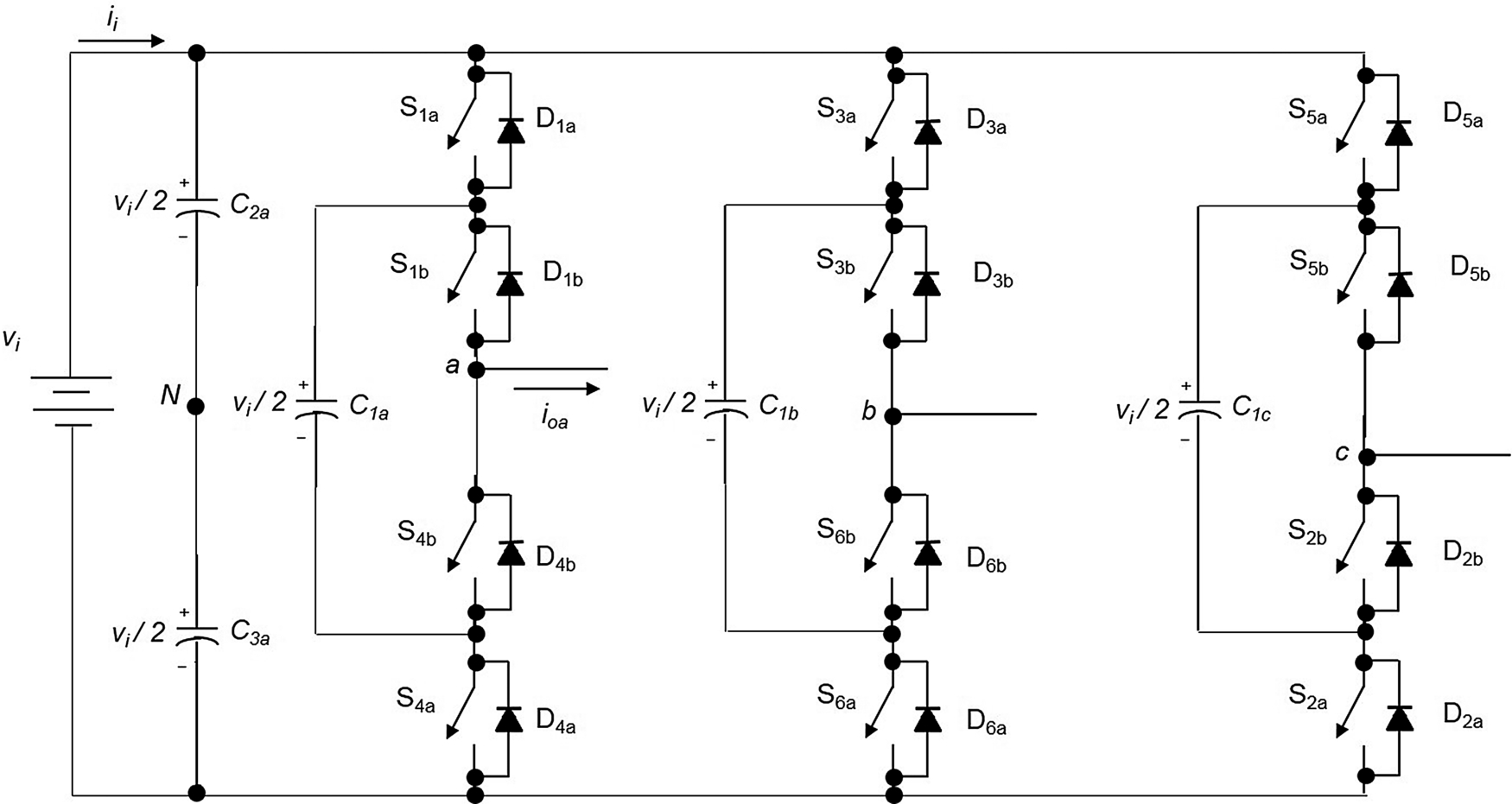
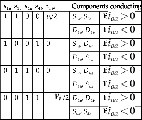
Table 11.9 is the switch state of the three-level inverter, just left leg. As it can be observed, not only always two switches are on, but also the signal S1a is the opposite of S4a, and S1b is the opposite of S4b. These conditions must be always satisfied. Table 11.9 shows that there is more than one switching state to produce the zero output level; this redundancy should be employed to distribute the losses or to regulate the capacitor voltages. Moreover, as the number of levels increase, more redundancy exists at different levels.
Table 11.9
Valid switch states for the three-level flying capacitors inverter, left leg
| s1a | s1b | s4a | s4b | vaN | Components conducting | |
| 1 | 1 | 0 | 0 | vi/2 | S1a, S1b | If ioa>0 |
| D1a, D1b | If ioa<0 | |||||
| 1 | 0 | 0 | 1 | 0 | S1a, D4b | If ioa>0 |
| D1a, S4b | If ioa<0 | |||||
| 0 | 1 | 1 | 0 | 0 | S1b, D4a | If ioa>0 |
| D1b, S4a | If ioa<0 | |||||
| 0 | 0 | 1 | 1 | −vi |
D4a, D4b | If ioa>0 |
| S4a, S4b | If ioa<0 | |||||
11.5.1.3 Casacade Inverter
In Fig. 11.44, the cascade inverter is shown (five levels). This topology is based on several full-bridge single-phase voltage-source inverters with their output connected in series. An M-level inverter requires (M−1)/2 single-phase full-bridge VSI per leg and 2(M−1) switching semiconductors per leg, but no additional diodes are required. Also M−1 switches per leg must be on to select the desired level.
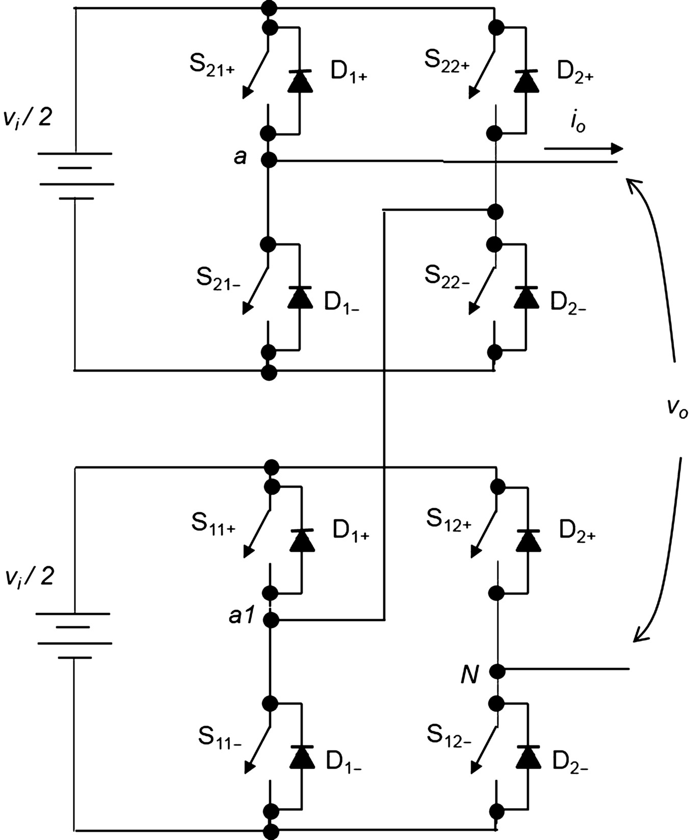
Table 11.10 gives the switch states of the five-level inverter. Notice that only the top switch control signals of each single-phase full-bridge VSI are shown. Their respective bottom switch control signals are complementary, in order to accomplish with the first compulsory rule for VSIs. As it can be observed, always four devices are on; notice that since a single-phase full-bridge inverter is used, the same rules apply for the control signals of the semiconductors. As it can be observed in Table 11.10, there are more than one switching state to produce some output levels; this redundancy should be employed to distribute the losses. Moreover, as the number of levels increases, more redundancy exists at different levels.
11.5.2 Current Source-Based Multilevel Topologies
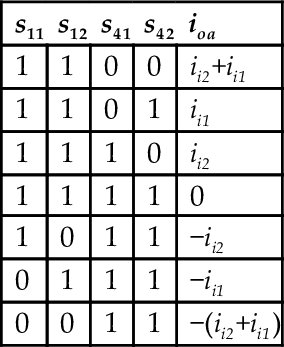
Duality is found in many aspects related to voltage- and current-source inverters. Perhaps, the most evident is the duality in terms of modulating techniques. Thus, current-source-based multilevel topologies are available as well. There are different topologies reported: paralleled, two-stage, and embedded configurations.
Fig. 11.45 shows a three-level M=3 current-source topology, which is formed by paralleling two three-phase CSI topologies, the named paralleled CSI (Table 11.11). The main goal is to share evenly the ac current ioabc among the two topologies (iabco/2=iabco1=iabc02![]() ). This should be ensured by having equal dc link currents (ii1=ii2
). This should be ensured by having equal dc link currents (ii1=ii2![]() ). Similarly to voltage-source-based multilevel topologies, this could be achieved either by using two independent dc link currents or by properly gating the power semiconductors.
). Similarly to voltage-source-based multilevel topologies, this could be achieved either by using two independent dc link currents or by properly gating the power semiconductors.

11.5.3 Modulation Techniques in Multilevel Inverters
As in traditional inverters, the sinusoidal pulse width and space-vector modulation can be employed in multilevel inverters, for both CSI and VSI.
11.5.3.1 The SPWM Technique
The main objective is to generate the appropriate gating signals so as to obtain fundamental inverter phase voltages or currents equal to a given set of modulating signals. Specifically, the SPWM in three-level VSIs uses a sinusoidal set of modulating signals (vca, vcb, and vcc for phases a, b, and c, respectively) and M−1=2 triangular type of carrier signals (vΔ1 and vΔ2) as illustrated in Fig. 11.46A. The best results are obtained if the carrier signals are in-phase (synchronized with the modulating signal) and feature an odd normalized frequency (e.g., mf=15![]() ). According to Fig. 11.46A and considering a neutral-point-clamped inverter (Fig. 11.42), the switch S1a is turned either on if vca>vΔ1
). According to Fig. 11.46A and considering a neutral-point-clamped inverter (Fig. 11.42), the switch S1a is turned either on if vca>vΔ1![]() or off if vca<vΔ1
or off if vca<vΔ1![]() , and switch S1b is turned either on if vca>vΔ2
, and switch S1b is turned either on if vca>vΔ2![]() or off if vca<vΔ2
or off if vca<vΔ2![]() . Additionally, the switch S4a status is obtained as the opposite to switch S1a, and the switch S4b status is obtained as the opposite to switch S1b. In order to use the same set of carrier signals to generate the gating signals for phases b and c, the normalized frequency of the carrier signal mf should be a multiple of 3. Thus, the possible values are mf=3,9,15,21,…
. Additionally, the switch S4a status is obtained as the opposite to switch S1a, and the switch S4b status is obtained as the opposite to switch S1b. In order to use the same set of carrier signals to generate the gating signals for phases b and c, the normalized frequency of the carrier signal mf should be a multiple of 3. Thus, the possible values are mf=3,9,15,21,…![]() .
.

 , ma=0.8
 ): (A) modulating and carrier signals, (B) switch S1a status, (C) switch S4b status, (D) inverter phase a voltage, (E) inverter phase a voltage spectrum, (F) load line voltage, (G) load line voltage spectrum, and (H) phase-load a voltage.
Fig. 11.46 shows the relevant waveforms for a three-level neutral-point-clamped inverter modulated by means of an SPWM technique (mf=15![]() , ma=0.8
, ma=0.8![]() ). Specifically, Fig. 11.46D shows the inverter phase voltage, which is clearly a three-level type of voltage, and Fig. 11.46F shows the load line voltage, which shows that the step voltages are at most vi/2. More importantly, the inverter phase voltage (Fig. 11.46E) contains harmonics at l⋅mf±k
). Specifically, Fig. 11.46D shows the inverter phase voltage, which is clearly a three-level type of voltage, and Fig. 11.46F shows the load line voltage, which shows that the step voltages are at most vi/2. More importantly, the inverter phase voltage (Fig. 11.46E) contains harmonics at l⋅mf±k![]() with l=1,3,…
with l=1,3,…![]() and k=0,2,4,…
and k=0,2,4,…![]() and at l⋅mf±k
and at l⋅mf±k![]() with l=2,4,…
with l=2,4,…![]() and k=1,3,…
and k=1,3,…![]() . For instance, the first set of harmonics (l=1
. For instance, the first set of harmonics (l=1![]() , mf=15
, mf=15![]() ) are at 15, 15±2
) are at 15, 15±2![]() , 15±4,…
, 15±4,…![]() . The inverter line voltage (Fig. 11.46G) contains harmonics at l⋅mf±k
. The inverter line voltage (Fig. 11.46G) contains harmonics at l⋅mf±k![]() with l=1,3,…
with l=1,3,…![]() and k=2,4,…
and k=2,4,…![]() and at l⋅mf±k
and at l⋅mf±k![]() with l=2,4,…
with l=2,4,…![]() and k=1,3,…
and k=1,3,…![]() . For instance, the first set of harmonics in the line voltages (l=1
. For instance, the first set of harmonics in the line voltages (l=1![]() , mf=15
, mf=15![]() ) are at 15±2
) are at 15±2![]() , 15±4,…
, 15±4,…![]() .
.
All the other features of carrier-based PWM techniques also apply in multilevel inverters. Firstly, the fundamental component of the inverter phase voltages satisfies
ˆvaN1=ˆvbN1=ˆvcN1=mavi20<ma≤1
and thus, the line voltages satisfy
ˆvab1=ˆvbc1=ˆvca1=ma√3vi20<ma≤1
where 0<ma≤1![]() is the linear operating region. To further increase the amplitude of the load voltages, the overmodulation operating region can be used by further increasing the modulating signal amplitudes (ma>1
is the linear operating region. To further increase the amplitude of the load voltages, the overmodulation operating region can be used by further increasing the modulating signal amplitudes (ma>1![]() ), where the line voltages range in
), where the line voltages range in
√3vi2<ˆvab1=ˆvbc1=ˆvca1<4π√3vi2
Second, the modulating signals could be improved by adding a third harmonic (zero sequence), which will increase the linear region up to ma=1.15![]() . This results in a maximum fundamental line-voltage component equal to vi; as a third point, a nonsinusoidal set of modulating signals could also be used by the modulating technique. This is the case where nonsinusoidal line voltages are required as in active filter applications, and finally, because of the two quadrants operation of VSIs, the multilevel inverter could equally be used in applications where the active power flow goes from the dc to the ac side or from the ac to the dc side.
. This results in a maximum fundamental line-voltage component equal to vi; as a third point, a nonsinusoidal set of modulating signals could also be used by the modulating technique. This is the case where nonsinusoidal line voltages are required as in active filter applications, and finally, because of the two quadrants operation of VSIs, the multilevel inverter could equally be used in applications where the active power flow goes from the dc to the ac side or from the ac to the dc side.
In general, for an M-level inverter modulated by means of a carrier-based technique, three modulating signals 120° out of phase and M−1 carrier signals are required. Key waveforms are shown in Fig. 11.47.
 , ma=0.8): (A) inverter phase a voltage, (B) inverter phase a voltage spectrum, (C) load line voltage, and (D) load line voltage spectrum.
One of the drawbacks of the multilevel inverter is that the dc link capacitor voltages or inductor currents, depending on the type of inverter, should be regulated. Unfortunately, this is not a natural operating condition mainly due to the fact that the storage elements are operated in a not symmetrical manner, and therefore, they will not equally share energy.
11.5.3.2 The SPWM Technique in Three-level CSIs
As in three-level VSIs, the main objective is to generate the appropriate 12 gating signals so as to obtain fundamental inverter line currents equal to a given set of modulating signals. Specifically, the SPWM in three-level inverters uses a sinusoidal set of modulating signals (ica, icb, and icc for phases a, b, and c, respectively) and N−1=2![]() triangular type of carrier signals (iΔ1 and iΔ2) as illustrated in Fig. 11.48A and E. The best results are obtained if the carrier signals are 180° out of phase and feature an odd normalized frequency (e.g., mf=15
triangular type of carrier signals (iΔ1 and iΔ2) as illustrated in Fig. 11.48A and E. The best results are obtained if the carrier signals are 180° out of phase and feature an odd normalized frequency (e.g., mf=15![]() ). In order to use the same set of carrier signals to generate the gating signals for phases b and c, the normalized frequency of the carrier signal mf should be a multiple of 3. Thus, the possible values are mf=3,9,15,21,…
). In order to use the same set of carrier signals to generate the gating signals for phases b and c, the normalized frequency of the carrier signal mf should be a multiple of 3. Thus, the possible values are mf=3,9,15,21,…![]() .
.
 , ma=0.8): (A) modulating signals and carrier signal 1, (B) switch S11 status, (C) inverter 1 linear current, (D) inverter 1 linear current spectrum, (E) modulating signals and carrier signal 2, (F) switch S12 status, (G) inverter 2 linear current, and (H) inverter 2 linear current spectrum.
Fig. 11.48 shows the relevant waveforms for a three-level inverter modulated by means of an SPWM technique (mf=15![]() , ma=0.8
, ma=0.8![]() ). Specifically, Fig. 11.48B and F show the gating signals obtained as described earlier in this chapter. The inverter line currents shown in Fig. 11.48C and G feature spectra shown in Fig. 11.48D and H, respectively. As expected, the inverter line currents contain harmonics at l⋅mf±k
). Specifically, Fig. 11.48B and F show the gating signals obtained as described earlier in this chapter. The inverter line currents shown in Fig. 11.48C and G feature spectra shown in Fig. 11.48D and H, respectively. As expected, the inverter line currents contain harmonics at l⋅mf±k![]() with l=1,3,…
with l=1,3,…![]() and k=2,4,…
and k=2,4,…![]() and at l⋅mf±k
and at l⋅mf±k![]() with l=2,4,…
with l=2,4,…![]() and k=1,3,…
and k=1,3,…![]() . For instance, the first set of harmonics in the line currents (l=
. For instance, the first set of harmonics in the line currents (l=![]() 1, mf=15
1, mf=15![]() ) are at 15±2
) are at 15±2![]() , 15±4,…
, 15±4,…![]() .
.
The total inverter line current is shown in Fig. 11.49A and features the first set of unwanted harmonics around 2mf (Fig. 11.49B). This becomes the first advantage of using a multilevel topology as the filtering component requirements become more relaxed. All the other features of carrier-based PWM techniques also apply in current-source multilevel inverters. For instance, (I) the fundamental component of the line currents satisfies
 , ma=0.8): (A) total inverter line current and (B) total inverter line current spectrum.
ˆioa1=ˆiob1=ˆioc1=ma√32(ii1+ii2)0<ma≤1
where 0<ma≤1![]() is the linear operating region. Also, (II) to further increase the amplitude of the load currents, a zero-sequence signal could be injected to the modulating signals, in this case,
is the linear operating region. Also, (II) to further increase the amplitude of the load currents, a zero-sequence signal could be injected to the modulating signals, in this case,
ˆioa1=ˆiob1=ˆioc1=ma√32(ii1+ii2)0<ma≤2/√3
the overmodulation operating region can be used by further increasing the modulating signal amplitudes (ma>2/√3![]() ), where the line currents range in
), where the line currents range in
(ii1+ii2)<ˆioa1=ˆiob1=ˆioc1<4π(ii1+ii2)
Also, (III) a nonsinusoidal set of modulating signals could also be used by the modulating technique. This is the case where nonsinusoidal line currents are required as in active filter applications, and (IV) because of the two quadrants operation of CSIs, the multilevel inverter could equally be used in applications where the active power flow goes from the dc to the ac side or from the ac to the dc side. In general, for an N-level inverter modulated by means of a carrier-based technique, three modulating signals 120° out of phase and N−1![]() carrier signals are required, and the line currents in the inverters have a peak value of ii/(N−1
carrier signals are required, and the line currents in the inverters have a peak value of ii/(N−1![]() ).
).
One of the drawbacks of the multilevel inverter is that the dc link capacitors cannot be supplied by a single dc voltage source. This is due to the fact that the currents required by the inverter in the dc bus are not symmetrical, and therefore, the capacitors will not equally share the dc supply voltage vi. To overcome this problem, two alternatives are developed later on.
11.5.3.3 The Space-Vector Modulation
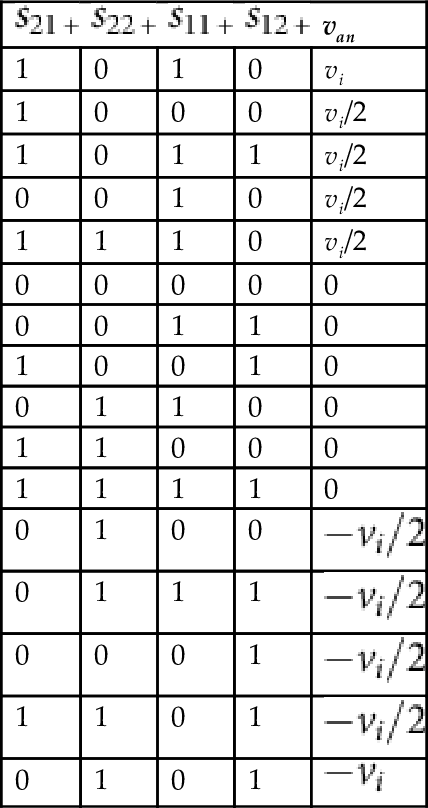
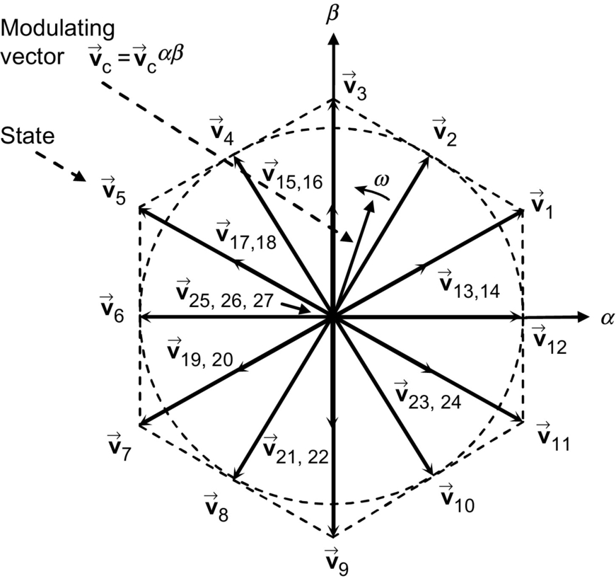
The SV modulating technique can be applied using the same principles used in two-level inverters. However, the higher number of voltage levels increases the complexity of the practical implementation of the technique. For instance, in M=3-level inverters, each leg allows M=3 different switch combinations as indicated in the previous sections. Therefore, in a three-phase system, there are M 3=27 total valid switch combinations, which generate M 3=27 load line voltages that are represented by M 3=27 space vectors (→v1![]() , →v2,…,→v27
, →v2,…,→v27![]() ) in Fig. 11.50. For instance, →v2=0.5+j0.866
) in Fig. 11.50. For instance, →v2=0.5+j0.866![]() is due to the line voltages vab=0.5
is due to the line voltages vab=0.5![]() , vbc=0.5
, vbc=0.5![]() , vca=−1.0
, vca=−1.0![]() in per unit. Thus, although the principle of operation is the same, the SV digital algorithm will have to deal with a higher number of states M 3. Moreover, because some space vectors (e.g., →v13
in per unit. Thus, although the principle of operation is the same, the SV digital algorithm will have to deal with a higher number of states M 3. Moreover, because some space vectors (e.g., →v13![]() and →v14
and →v14![]() in Fig. 11.50) produce the same load voltage terminals, the algorithm will have to decide between the two based on additional criteria and that of the basic SV approach. Clearly, as the number of level increases, the algorithm becomes more and more elaborate. However, the benefits are not evident as the number of level increases. The maximum number of levels used in practical applications is five. This is based on a compromise between the complexity of the implementation and the benefits of the resulting waveforms.
in Fig. 11.50) produce the same load voltage terminals, the algorithm will have to decide between the two based on additional criteria and that of the basic SV approach. Clearly, as the number of level increases, the algorithm becomes more and more elaborate. However, the benefits are not evident as the number of level increases. The maximum number of levels used in practical applications is five. This is based on a compromise between the complexity of the implementation and the benefits of the resulting waveforms.
11.5.3.4 Balancing Issues
The operation for the multilevel converter was made considering an even distribution of the voltage across the dc link capacitors or current of the inductors, depending of the type of inverter. This even distribution is not naturally achieved and could be overcome by supplying the storage elements from independent supplies or properly gating the power semiconductors of the inverter in order to minimize the unbalance.
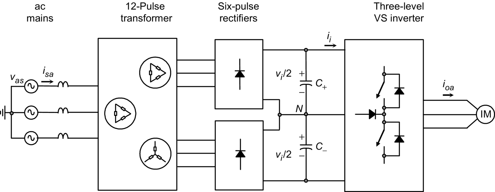
Fig. 11.51 shows an ASD based on a three-level VSI, where the dc link capacitors are feed from two different sources. This approach is being commercially used as it ensures a robust balanced dc link voltage distribution and operates with a high-performance type of ac main current. Indeed, for an M-level inverter, M−1-independent dc voltage supplies are required that could be provided by M−1 six-pulse rectifiers feed from an M−1 pulse transformer. Therefore, the ac main currents are an M−1-level type of waveform.
This approach cannot be used when the inverter does not feature dc link voltage supplies. This is the case of static power reactive power compensators and static power active filters. In this case, the proper gating of the power semiconductors becomes the only choice to keep and balance the dc link voltages. Fig. 11.52A shows this case where the current added by the inverter ioabc provides the reactive power and current harmonics such that the ac main current isabc features a given power factor.
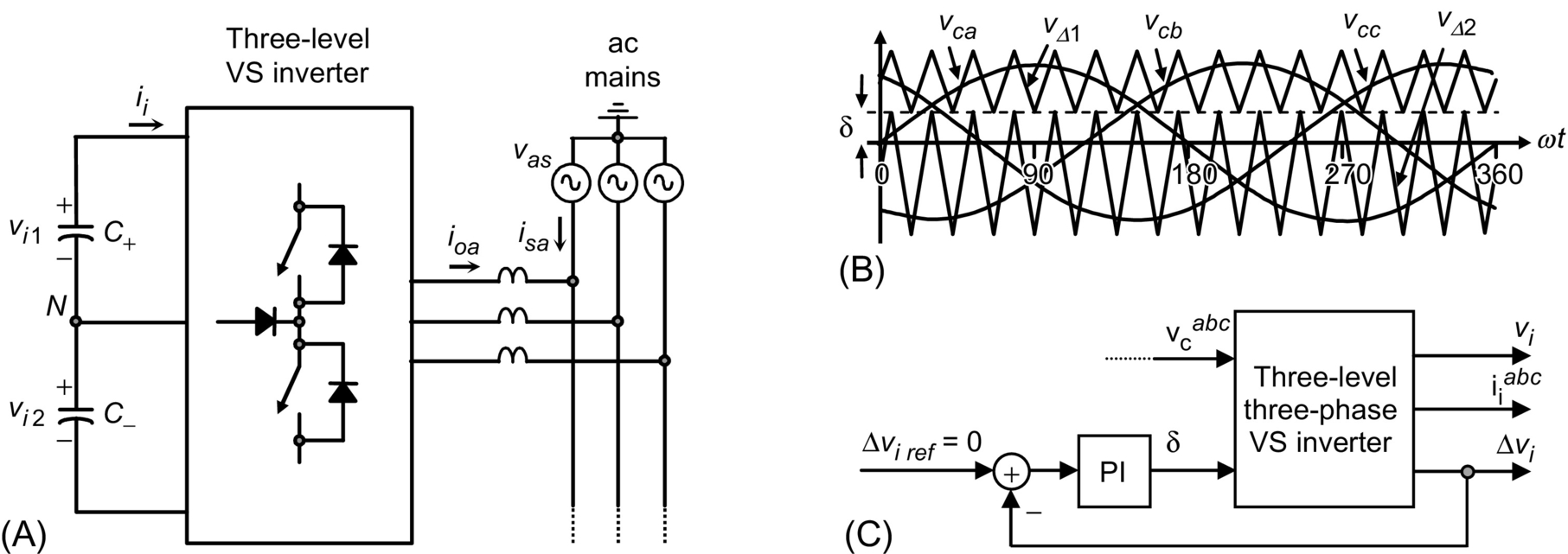
The SPWM modulating technique could be used as in Fig. 11.46; however, the zero level of the carrier δ is left as a manipulable variable in Fig. 11.52B. In fact, it is used to control the difference of the upper and lower capacitor voltages Δvi=vi1−vi2![]() . A closed-loop alternative is depicted in Fig. 11.52C to manipulate δ. The modulating signals vcabc are left to control the reactive power and current harmonics injected into the ac mains by regulating the currents ioabc and keep the total dc link voltage vi=vi1+vi2
. A closed-loop alternative is depicted in Fig. 11.52C to manipulate δ. The modulating signals vcabc are left to control the reactive power and current harmonics injected into the ac mains by regulating the currents ioabc and keep the total dc link voltage vi=vi1+vi2![]() equal to a reference. Both loops are not included in Fig. 11.52C.
equal to a reference. Both loops are not included in Fig. 11.52C.
11.6 Closed-Loop Operation of Inverters
In the inverter, as a classic power converter, the output depends on different conditions. For instance, in ASDs, the load usually changes, so the ac waveforms should be adjusted to these new conditions. Also, as the dc power supplies are not ideal and the dc quantities are not fixed, the inverter should compensate for such variations. Such adjustments can be done automatically by means of a closed-loop approach. Inverters also provide an alternative to changing the load operating conditions.
There are two alternatives for closed-loop operation, the feedback and the feedforward approaches. It is known that the feedback approach can compensate for both the perturbations (dc power variations) and the load variations (load torque changes). However, the feedforward strategy is more effective in mitigating perturbations as it prevents its negative effects at the load side. These cause-effect issues are analyzed in three-phase inverters in the following, although similar results are obtained for single-phase VSIs.
11.6.1 Feedforward Techniques in Voltage Source Inverters
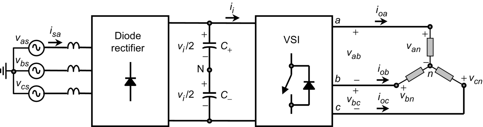
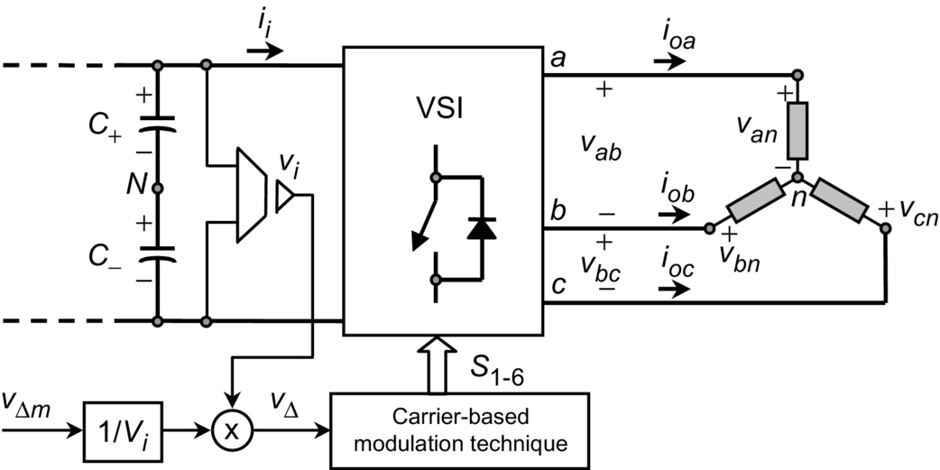
The dc link bus voltage in VSIs is usually considered a constant-voltage source vi. Unfortunately and due to the fact that most practical applications generate the dc bus voltage by means of a diode rectifier (Fig. 11.53), the dc bus voltage contains low-order harmonics such as the sixth, twelfth, … (due to six-pulse diode rectifiers) and the second harmonic if the ac voltage supply features an unbalance, which is usually the case. Additionally, if the three-phase load is unbalanced, as in UPS applications, the dc input current in the inverter ii also contains the second harmonic, which in turn contributes to the generation of a second voltage harmonic in the dc bus.
The basic principle of feedforward approaches is to sense the perturbation and then modify the input in order to compensate for its effect. In this case, the dc link voltage should be sensed, and the modulating technique should accordingly be modified. The fundamental ab line voltage in a VSI SPWM can be written as
vab1(t)={vca1(t)ˆvΔ−vcb1(t)ˆvΔ}√32vi(t)ˆvΔ>ˆvca1,ˆvcb1
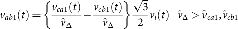
where ˆvΔ![]() is the carrier signal peak, ˆvca1
is the carrier signal peak, ˆvca1![]() and ˆvcb1
and ˆvcb1![]() are the modulating signal peaks, and vca(t) and vcb(t) are the modulating signals. If the dc bus voltage vi varies around a nominal Vi value, then the fundamental line voltage varies proportionally; however, if the carrier signal peak ˆvΔ
are the modulating signal peaks, and vca(t) and vcb(t) are the modulating signals. If the dc bus voltage vi varies around a nominal Vi value, then the fundamental line voltage varies proportionally; however, if the carrier signal peak ˆvΔ![]() is redefined as
is redefined as
ˆvΔ=ˆvΔmvi(t)Vi

where ˆvΔm![]() is the carrier signal peak (Fig. 11.54), then the resulting fundamental ab line voltage in a VSI SPWM is
is the carrier signal peak (Fig. 11.54), then the resulting fundamental ab line voltage in a VSI SPWM is
vab1(t)={vca1(t)ˆvΔm−vcb1(t)ˆvΔm}√32Vi

where, clearly, the result does not depend upon the variations of the dc bus voltage.
Fig. 11.55 shows the waveforms generated by the SPWM under a severe dc bus voltage variation (a second harmonic has been added manually to a constant Vi). As a consequence, the ac line voltage generated by the VSI is distorted as it contains low-order harmonics (Fig. 11.55E). These operating conditions may not be acceptable in standard applications such as ASDs because the load will draw distorted three-phase currents as well. The feedforward loop performance is illustrated in Fig. 11.56. As expected, the carrier signal is modified so as to compensate for the dc bus voltage variation (Fig. 11.56B). This is probed by the spectrum of the ac line voltage that does not contain low-order harmonics (Fig. 11.56E). It should be noted that ˆvΔ>ˆvca1,ˆvcb1![]() ; therefore, the compensation capabilities are limited by the required ac line voltage.
; therefore, the compensation capabilities are limited by the required ac line voltage.
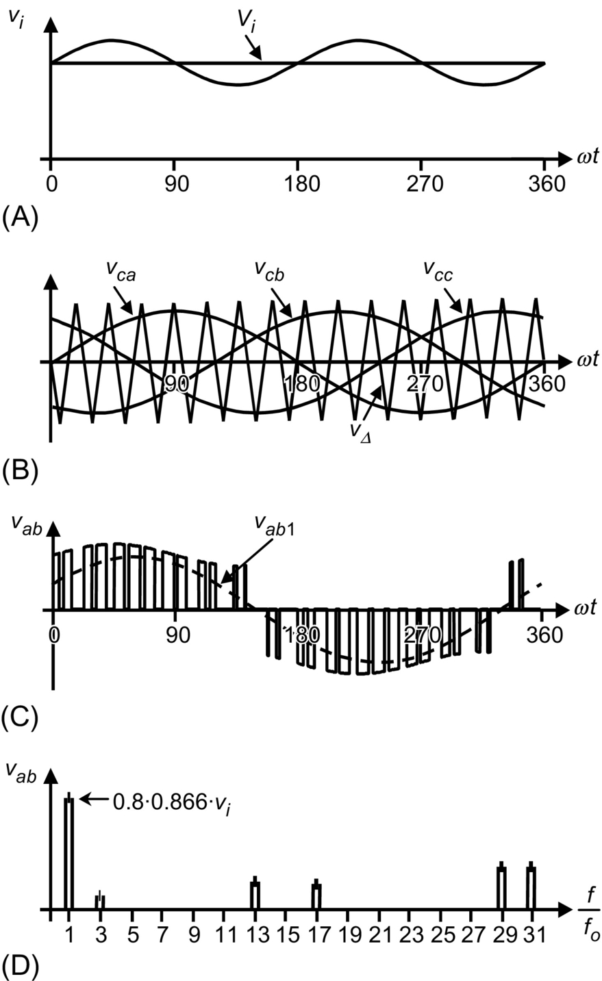 , mf=9
 ): (A) dc bus voltage, (B) carrier and modulating signals, (C) ac output voltage, and (D) ac output voltage spectrum.
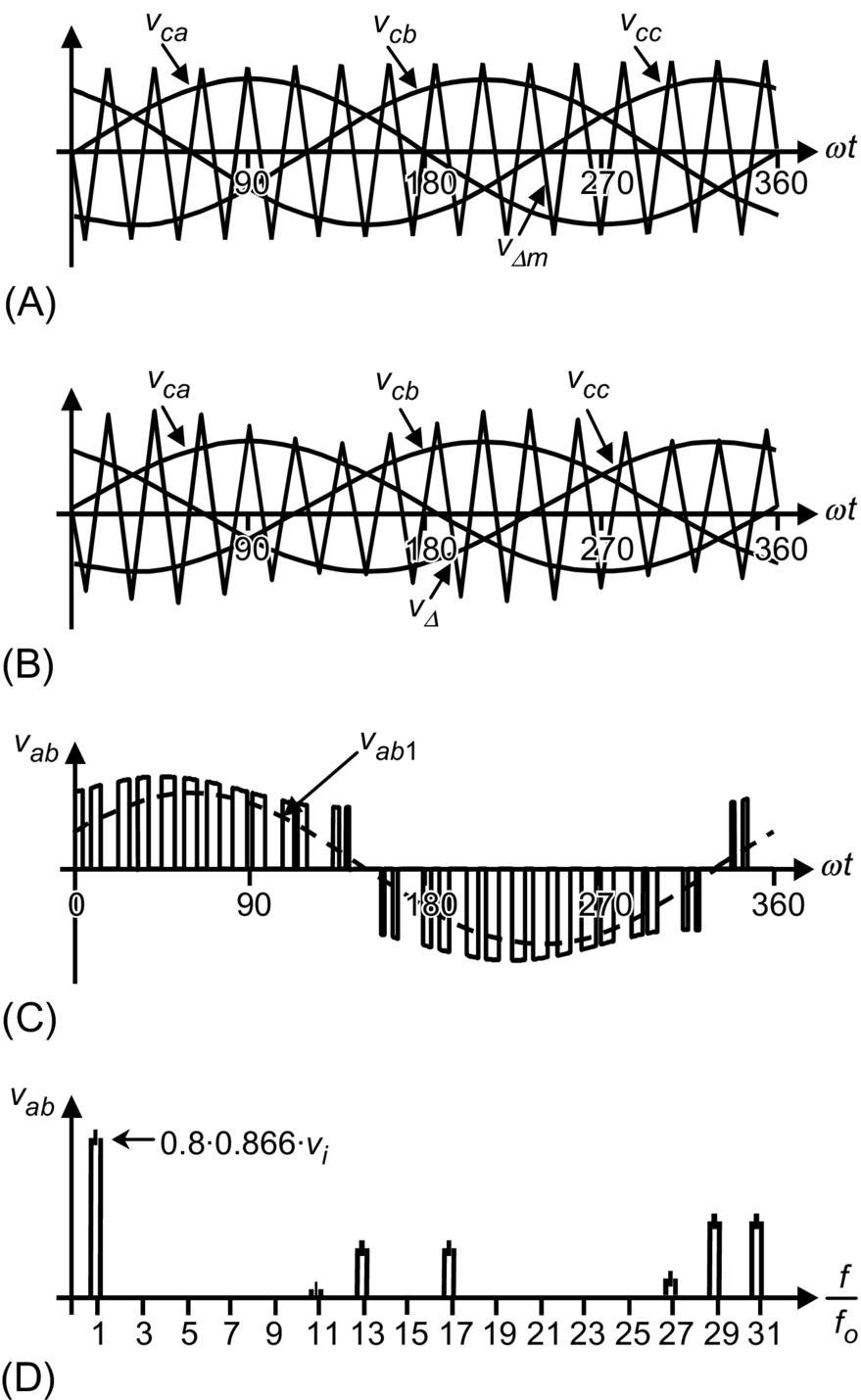 , mf=9): (A) carrier and modulating signals, (B) modified carrier and modulating signals, (C) ac output voltage, and (D) ac output voltage spectrum.
The performance of the feedforward approach depends upon the frequency of the harmonics present in the dc bus voltage and the carrier signal frequency. Fortunately, the relevant unwanted harmonics to be found in the dc bus voltage are the second, due to unbalanced supply voltages, and/or the sixth as the dc bus voltage is generated by means of a six-pulse diode rectifier. Therefore, a carrier signal featuring a 15-pu frequency is found to be sufficient to properly compensate for dc bus voltage variations.
Unbalanced loads generate a dc input current ii that contains a second harmonic, which contributes to the dc bus voltage variation. The previous feedforward approach can compensate for such perturbation and maintain balanced ac load voltages.
Digital techniques can also be modified in order to compensate for dc bus voltage variations by means of a feedforward approach.
The duality principle between the voltage- and the current-source inverters indicates that, as described previously, the feedforward approach can be also used for CSIs and for VSIs. Therefore, low-order harmonics present in the dc bus current can be compensated for before they appear at the load side. This can be done for both analog-based (e.g., carrier-based) and digital-based (e.g., space-vector) modulating techniques.
11.6.2 Feedback Techniques in Voltage Source Inverters
Unlike the feedforward advantages, the feedback techniques are more effective to regulate than the system output by gating signals of the inverters properly. Another important difference is that feedback techniques need to sense the controlled variables. In general, the controlled variables (output to the system) are chosen according to the control objectives. For instance, in ASDs, it is usually necessary to keep the motor line currents equal to a given set of sinusoidal references. Therefore, the controlled variables become the ac line currents. There are several alternatives to implement feedback techniques in VSIs, and three of them are discussed next.
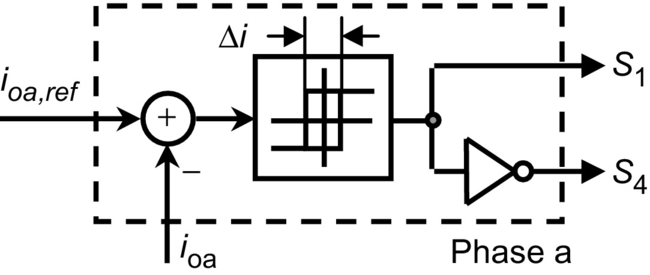
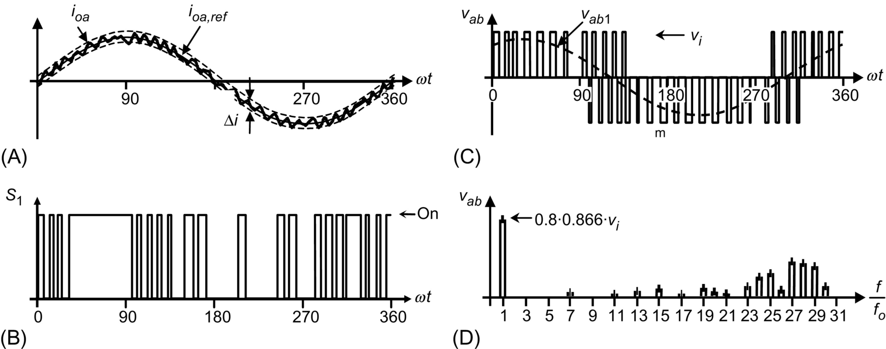
11.6.2.1 Hysteresis Current Control
The main purpose here is to force the ac line current to follow a given reference. The status of the power semiconductors are changed whenever the actual ioa current goes beyond a given reference ioa,ref±Δi/2![]() . Fig. 11.57 shows the hysteresis current controller for one phase. Identical controllers are used in the other phases. The implementation of this controller is simple as it requires a simple comparator operating in the hysteresis mode; thus, the controller and modulator are combined in one unit.
. Fig. 11.57 shows the hysteresis current controller for one phase. Identical controllers are used in the other phases. The implementation of this controller is simple as it requires a simple comparator operating in the hysteresis mode; thus, the controller and modulator are combined in one unit.
Unfortunately, there are several drawbacks associated with the technique itself. First, the switching frequency cannot be predicted as in carrier-based modulators, and therefore, the harmonic content of the ac line voltages and currents becomes random (Fig. 11.58D). This could be a disadvantage when designing the filtering components. Second, as three-phase loads do not have the neutral connected as in ASDs, the load currents add up to zero. This means that only two ac line currents can be controlled independently at any given instant. Therefore, one of the hysteresis controllers is redundant at a given time. This explains why the load current goes beyond the limits and introduces limit cycles (Fig. 11.58A). Finally, although the ac load currents add up to zero, the controllers cannot ensure that all load line currents feature a zero dc component in one load cycle.
11.6.2.2 Linear Control of VSIs
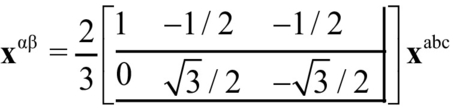
Proportional and proportional-integrative controllers can also be used in VSIs by employing a transformation. The main purpose is to generate the modulating signals vca, vcb, and vcc in a closed-loop fashion as depicted in Fig. 11.59. The modulating signals can be used by a carrier-based technique such as the SPWM (as depicted in Fig. 11.59) or by space-vector modulation. Because the load line currents add up to zero, the load line current references must add up to zero. Thus, the abc/ αβγ transformation can be used to reduce to two controllers the overall implementation scheme as the γ component is always zero. This avoids limit cycles in the ac load currents.

The transformation of a set of variables in the stationary abc frame xabc into a set of variables in the stationary αβ frame xαβ is given by
The selection of the controller (P, PI, …) is done according to the control procedures such as steady-state error, settling time, and overshoot. Fig. 11.60 shows the relevant waveforms of a VSI SPWM controlled by means of a PI controller as shown in Fig. 11.59.
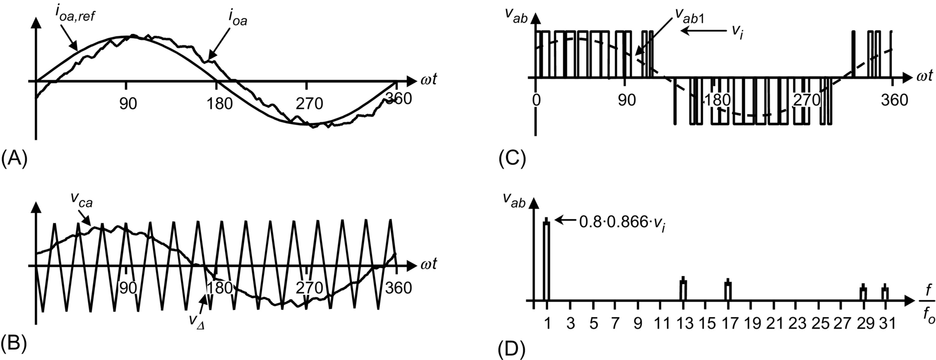 , mf=15): (A) actual ac load current and reference, (B) carrier and modulating signals, (C) ac output voltage, and (D) ac output voltage spectrum.
Although it is difficult to prove that no limit cycles are generated, the ac line current appears very much sinusoidal. Moreover, the ac line voltage generated by the VSI preserves the characteristics of such waveforms generated by SPWM modulators.
However, an error between the actual ioa and the ac line current reference ioa,ref can be observed (Fig. 11.60A). This error is inherent to linear controllers and cannot be totally eliminated, but it can be minimized by increasing the gain of the controller. However, the noise in the circuit is also increased, which could deteriorate the overall performance of the control scheme. The inherent presence of the error in this type of controllers is due to the fact that the controller needs a sinusoidal error to generate sinusoidal modulating signals vca, vcb, and vcc, as required by the modulator. Therefore, an error must exist between the actual and the ac line current references.
Nevertheless, as current-controlled VSIs are actually the inner loops in many control strategies, their inherent errors are compensated by the outer loop. This is the case of ASDs, where the outer speed loop compensates the inner current loops. In general, if the outer loop is implemented with dc quantities (such as speed), it can compensate the ac inner loops (such as ac line currents). If it is mandatory that a zero steady-state error be achieved with the ac quantities, then a stationary (abc frame) to rotating (dq frame) transformation is a valid alternative to use.
11.6.2.3 Linear Control of VSIs in a Rotating Frame
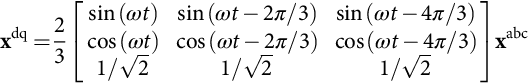
The rotating dq transformation allows ac three-phase circuits to be operated as if they were dc circuits. This is based upon a mathematical operation, that is, the transformation of a set of variables in the stationary abc frame xabc into a set of variables in the rotating dq0 frame xdq0. The transformation is given by
xdq=23[sin(ωt)sin(ωt−2π/3)sin(ωt−4π/3)cos(ωt)cos(ωt−2π/3)cos(ωt−4π/3)1/√21/√21/√2]xabc
where ω is the angular frequency of the ac quantities. For instance, the current vector given by
iabc=[iaibic]=[Isin(ωt−φ)Isin(ωt−2π/3−φ)Isin(ωt−4π/3−φ)]

becomes the vector
idq0=[idiqi0]=[Icos(φ)−Isin(φ)0]
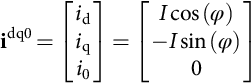
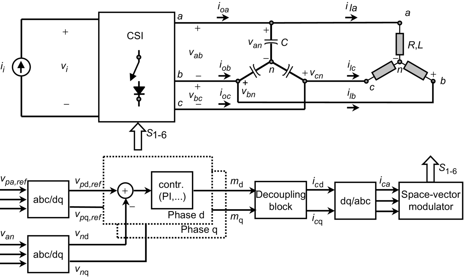
where I and φ are the amplitude and phase of the line currents, respectively. It can be observed that (a) the zero-component i0 is always zero as the three-phase quantities add up to zero and (b) the d and q components id, iq are dc quantities. Thus, linear controllers should help to achieve zero steady-state error. The control strategy shown in Fig. 11.61 is an alternative where the zero-component controller has been eliminated due to the fact that the line currents at the load side add up to zero.

The controllers in Fig. 11.61 include an integrator that generates the appropriate dc outputs md and mq even if the actual and the line current references are identical. This ensures that the zero steady-state error is achieved. The decoupling block in Fig. 11.61 is used to eliminate the cross coupling effect generated by the dq0 transformation and to allow an easier design of the parameters of the controllers.
The dq0 transformation requires the intensive use of multiplications and trigonometric functions. These operations can readily be done by means of digital microprocessors. Also, analog implementations would indeed be involved.
11.6.3 Feedback Techniques in Current Source Inverters
Duality indicates that CSIs should be controlled as equally as VSIs except that the voltages become currents and the currents become voltages. Thus, hysteresis, linear, and dq linear-based control strategies are also applicable to CSIs; however, the controlled variables are the load voltages instead of the load line currents.
For instance, the linear control of a CSI based on a dq transformation is depicted in Fig. 11.62. In this case, a passive balanced load is considered. In order to show that zero steady-state error is achieved, the per phase equations of the converter are written as
Cddtvabcp=iabco−iabcl
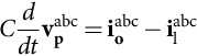
Lddtiabcl=vabcp−Riabcl

The ac line currents are in fact imposed by the modulator, and they satisfy
iabco=iiiabcc
Replacing Eq. (11.73) into the model of the converter Eqs. (11.71) and (11.72), using the dq0 transformation and assuming null zero component, the model of the converter becomes
ddtvdqp=−Wvdqp+iiCidqc−1Cidql
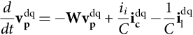
ddtidql=−Widql+1Lvdqp−RLidql
where W is given by
W=[0−ωω0]
A first approximation is to assume that the decoupling block is not there; in other words, idqc=mdq![]() . On the other hand, the model of the controllers can be written as
. On the other hand, the model of the controllers can be written as
mdq=k{vdqp,ref−vdqp}+1Tt∫−∞(vdqp,ref−vdqp)dt

where k and T are the proportional and integrative gains of the PI controller that are chosen to achieve a desired dynamic response. Combining the model of the controllers and the model of the converter in dq coordinates and using the Laplace transform, the following relationship between the reference and actual phase-load voltages is found:
vdqp=iiC{sk+1T}{sI+W+RLI}×[{sI+W+RLI}{s2I+s(W+iiCkI)+iiCTI}+sLCI]−1vdqp,ref

Finally, in order to prove that the zero steady-state error is achieved for step inputs in either the d or q component of the phase-load voltage reference, the previous expression is evaluated in s=0![]() . This results in the following:
. This results in the following:
vdqp=iiC{1T}{W+RLI}[{W+RLI}{iiCTI}]−1vdqp,ref=vdqp,ref

As expected, the actual and reference values are identical. Finally, the relationship in Eq. (11.78) is a matrix that is not diagonal. This means that both the actual and the reference phase-load voltages are coupled. In order to obtain a decoupled control, the decoupling block in Fig. 11.62 should be properly chosen.
11.7 Regeneration in Inverters
Industrial applications are usually characterized by a power flow that goes from the ac distribution system to the load. This is, for example, the case of an ASD operating in the motoring mode. In this instance, the active power flows from the dc side to the ac side of the inverter. However, there are an important number of applications in which the load may supply power to the system. Moreover, this could be an occasional condition and a normal operating condition. This is known as the regenerative operating mode. For example, when an ASD reduces the speed of an electric machine, this can be considered a transient condition. Downhill belt conveyors in mining applications can be considered as a normal operating condition. In order to simplify the notation, it could be said that an inverter operates in the motoring mode when the power flows from the dc to the ac side and in the regenerative mode when the power flows from the ac to the dc side.
11.7.1 Motoring Operating Mode in Three-phase VSIs
This is the case where the power flows from the dc side to the ac side of the inverter. Fig. 11.63 shows a simplified scheme of an ASD where the motor has been modeled by three RLe branches, where the sources eabc are the back emf. Because the ac line voltages applied by the inverter are imposed by the pulse width modulation technique being used, they can be adjusted according to specific requirements. In particular, Fig. 11.64 shows the relevant waveforms in a steady state for the motoring operating mode of the ASD. To simplify the analysis, a constant dc bus voltage vi=Vi![]() has been considered.
has been considered.
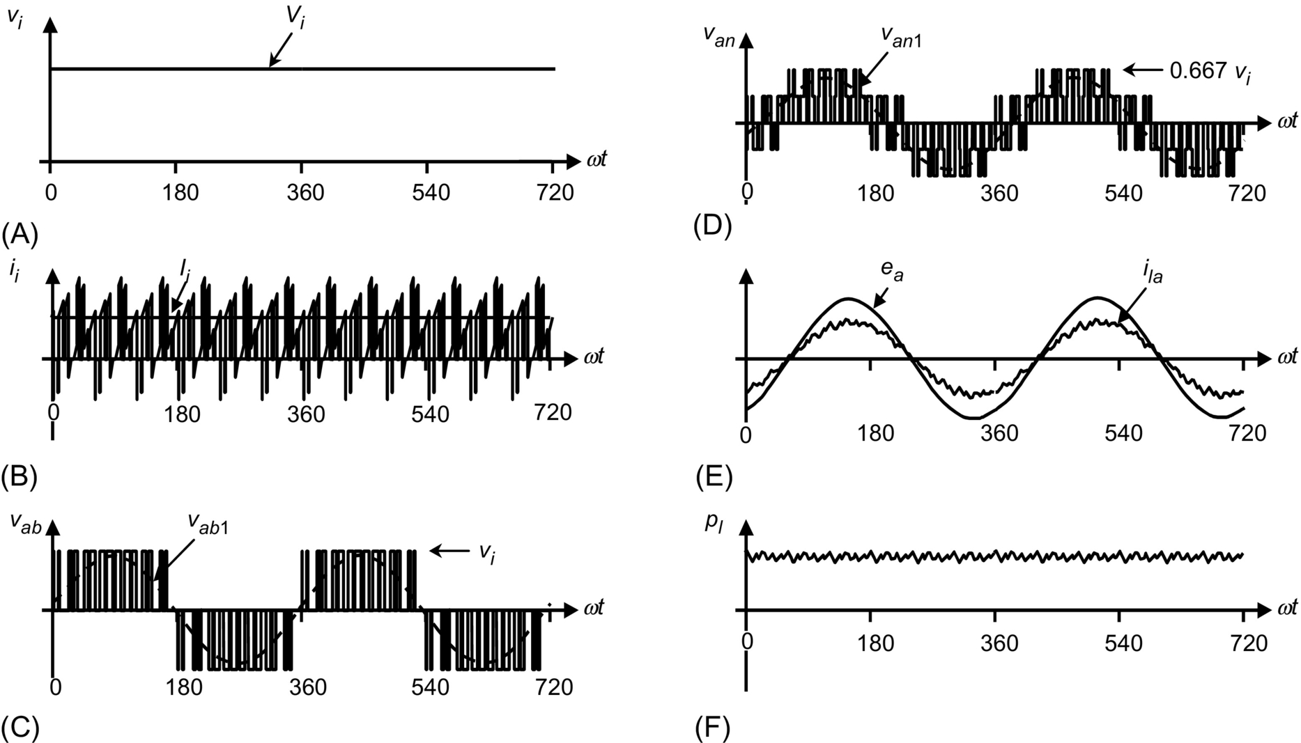
It can be observed that (i) the dc bus current ii features a dc value Ii that is positive and (ii) the motor line current is in phase with the back emf. Both features confirm that the active power flows from the dc source to the motor. This is also confirmed by the shaft power plot (Fig. 11.64F), which is obtained as
pl(t)=ea(t)ila(t)+eb(t)ilb(t)+ec(t)ilc(t)
11.7.2 Regenerative Operating Mode in Three-phase VSIs
The back emf sources eabc are functions of the machine speed, and as such, they ideally change just as the speed changes. The regeneration operating mode can be achieved by properly modifying the ac line voltages applied to the machine. This is done by the speed outer loop that could be based on a scalar (e.g., V/f) or vectorial (e.g., field-oriented) control strategy. As indicated earlier, there are two cases of regenerative operating modes.
11.7.2.1 Occasional Regenerative Operating Mode
This mode is required during transient conditions such as in occasional braking of electric machines (ASDs). Specifically, the speed needs to be reduced, and the kinetic energy is taken into the dc bus. Because the motor line voltage is imposed by the VSI, the speed reduction should be done in such a way that the motor line currents do not exceed the maximum values. This boundary condition will limit the ramp-down speed to a minimum, but shorter braking times will require a mechanical braking system.
Fig. 11.65 shows a transition from the motoring to regenerative operating mode for an ASD as shown in Fig. 11.63. Here, a stiff dc bus voltage has been used. Zone I in Fig. 11.65 is the motoring mode, zone II is a transition condition, and zone III is the regeneration mode. The line voltage is adjusted dynamically to obtain nominal motor line currents during regeneration (Fig. 11.65D). Zone III clearly shows that the shaft power gets reversed.

Occasional regeneration means that the drive rarely goes into this operating mode. Therefore, such energy can be (a) left uncontrolled or (b) burned in resistors that are paralleled to the dc bus. The first option is used in low- to medium-power applications that use diode-based front-end rectifiers. Therefore, the dc bus current flows into the dc bus capacitor, and the dc bus voltage rises accordingly to
Δvi=1CIiΔt
where Δvi is the dc bus voltage variation, C is the dc bus voltage capacitor, Ii is the average dc bus current during regeneration, and Δt is the duration of the regeneration operating mode. Usually, the drives have the capacitor C designed to allow a 10% overvoltage in the dc bus.
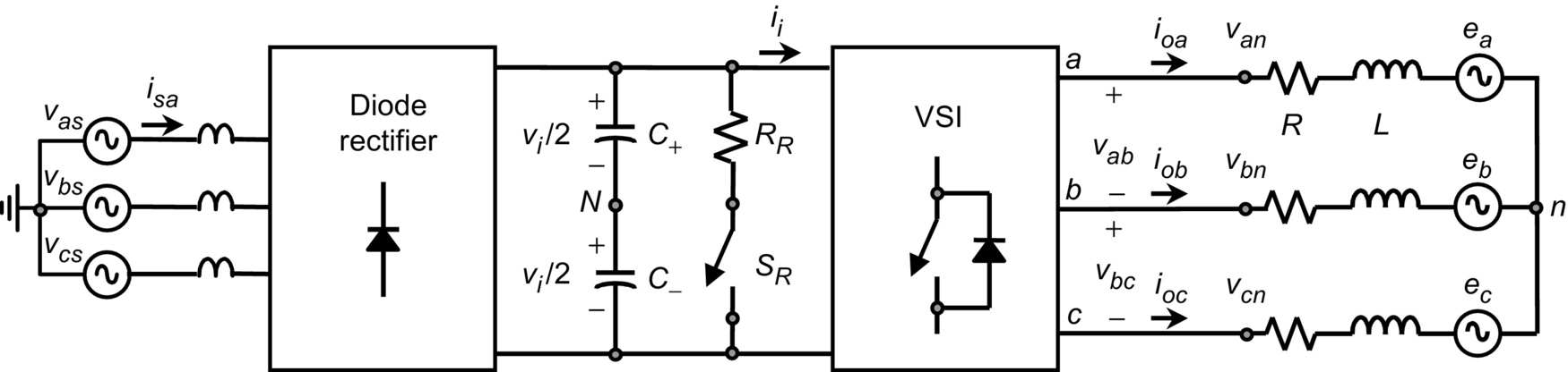
The second option uses burning resistors RR that are paralleled in the dc bus as shown in Fig. 11.66 by means of the switch SR. A closed-loop strategy based on the actual dc bus voltage modifies the duty cycle of the turn-on/turnoff of the switch SR in order to keep such voltage under a given reference. This alternative is used when the energy recovered by the VSI would result in an acceptable dc bus voltage variation if an uncontrolled alternative is used.
There are some special cases where the regeneration operating mode is frequently used. For instance, electric shovels in mining companies have repetitive working cycles, and ≈15%![]() of the energy is sent back into the dc bus. In this case, a valid alternative is to send back the energy into the ac distribution system.
of the energy is sent back into the dc bus. In this case, a valid alternative is to send back the energy into the ac distribution system.
The schematic shown in Fig. 11.67 is capable of taking the kinetic energy and sending it into the ac grid. As reviewed earlier, the regeneration operating mode reverses the polarity of the dc current ii, and because the diode-based front-end converter cannot take negative currents, a thyristor-based front-end converter is added. Similarly to the burning resistor approach, a closed-loop strategy based on the actual dc bus voltage vi modifies the commutation angle α of the thyristor rectifier in order to keep such voltage under a given reference.

11.7.2.2 Regenerative Operating Mode as Normal operating Mode
Fewer industrial applications are capable of returning energy into the ac distribution system on a continuous basis. For instance, mining companies usually transport their product downhill for a few kilometers before processing it. In such cases, the drive maintains the transportation belt conveyor at constant speed and takes the kinetic energy. Due to the large amount of energy and the continuous operating mode, the drive should be capable of taking the kinetic energy, transforming it into electric energy, and sending it into the ac distribution system. This would make the drive a generator that would compensate for the active power required by other loads connected to the electric grid.
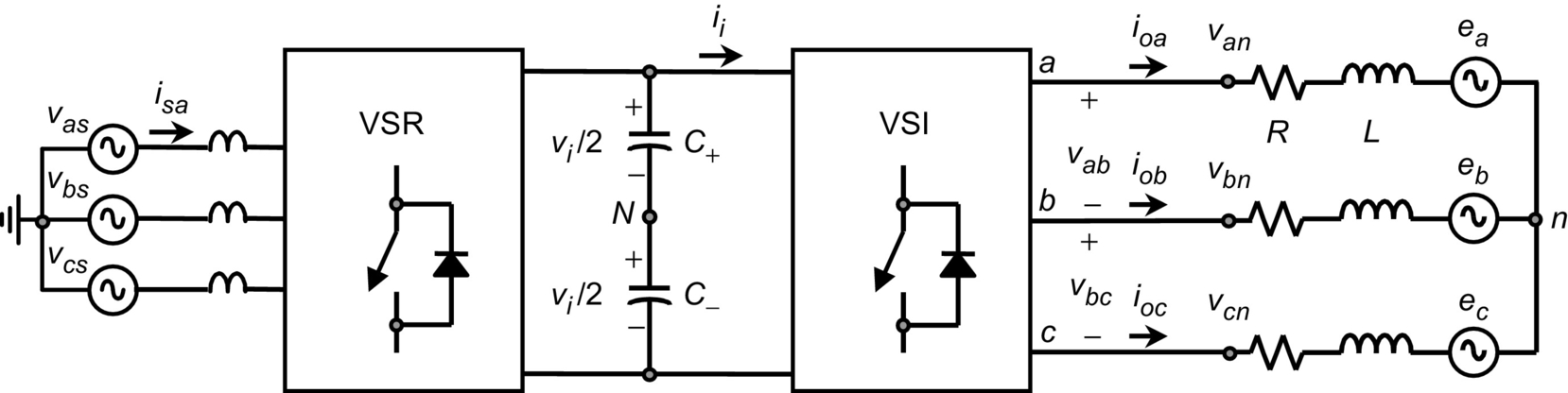
The schematic shown in Fig. 11.68 is a modern alternative for adding regeneration capabilities to the VSI-based drive on a continuous basis. In contrast to the previous alternatives, this scheme uses a VSI topology as an active front-end converter, which is generally called voltage-source rectifier (VSR). The VSR operates in two quadrants, that is, positive dc voltages and positive/negative dc currents as reviewed earlier. This feature makes it a perfect match for ASDs based on a VSI. Some of the advantages of using a VSR topology are the following: (i) The ac supply current can be as sinusoidal as required (by increasing the switching frequency of the VSR or the ac line inductance), (ii) the operation can be done at a unity displacement power factor in both motoring and regenerative operating modes, and (iii) the control of the VSR is done in both motoring and regenerative operating modes by a single dc bus voltage loop.
11.7.3 Regenerative Operating Mode in Three-phase CSIs
There are drives where the motor side converter is a CSI. This is usually the case where near sinusoidal motor voltages are needed instead of the PWM type of waveform generated by VSIs. This is normally the case for medium-voltage applications. Such inverters require a dc current source that is constructed by means of a controlled rectifier.
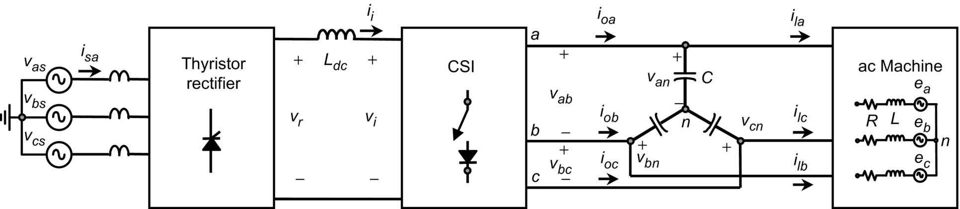
Fig. 11.69 shows a CSI-based ASD where the dc current source is generated by means of a thyristor-based rectifier in combination with a dc link inductor Ldc. In order to maintain a constant dc link current ii=Ii![]() , the thyristor-based rectifier adjusts the commutation angle α by means of a closed-loop control strategy. Assuming a constant dc link current, the regenerating operating mode is achieved when the dc link voltage vi reverses its polarity. This can be done by modifying the PWM pattern applied to the CSI as in the VSI-based drive. To maintain the dc link current constant, the thyristor-based rectifier also reverses its dc link voltage vr. Fortunately, the thyristor rectifier operates in two quadrants, that is, positive dc link currents and positive/negative dc link voltages. Thus, no additional equipment is required to include regeneration capabilities in CSI-based drives.
, the thyristor-based rectifier adjusts the commutation angle α by means of a closed-loop control strategy. Assuming a constant dc link current, the regenerating operating mode is achieved when the dc link voltage vi reverses its polarity. This can be done by modifying the PWM pattern applied to the CSI as in the VSI-based drive. To maintain the dc link current constant, the thyristor-based rectifier also reverses its dc link voltage vr. Fortunately, the thyristor rectifier operates in two quadrants, that is, positive dc link currents and positive/negative dc link voltages. Thus, no additional equipment is required to include regeneration capabilities in CSI-based drives.
Similarly, an active front-end rectifier could be used to improve the overall performance of the thyristor-based rectifier. A PWM current-source rectifier (CSR) could replace the thyristor-based rectifier with the following added advantages: (i) The ac supply current can be as sinusoidal as required (e.g., by increasing the switching frequency of the CSR), (ii) the operation can be done at a unity displacement power factor in both motoring and regenerative operating modes, and (iii) the control of the CSR is done in both motoring and regenerative operating modes by a single dc bus current loop.