
Linear and Nonlinear Control of Switching Power Converters
José Fernando Silva Universidade de Lisboa, Lisboa, Portugal
Sónia F. Pinto Universidade de Lisboa, Lisboa, Portugal
Abstract
This chapter provides tools to control switching electronic power converters. It starts by explaining techniques to obtain linear state-space converter models, illustrating them through examples. Linear models are then used to design linear feedback controllers for converter operating in the continuous or discontinuous mode.
Nonlinear state-space models and sliding-mode controllers are next used to define exactly the variables to be measured while providing the control and switching laws aiming for robust modulator and controller design.
Predictive control uses a detailed nonlinear dynamic model to forecast the converter future behavior upon application of every possible converter switching state or vector. The best vector is then applied to the converter by computing the minimum of a cost functional.
Fuzzy control needs an expert qualitative knowledge of the converter dynamics. The steps to obtain a fuzzy controller are described, and the provided example compares the fuzzy controller performance to current-mode control.
The backstepping control methodology is explained using a recursive procedure interconnecting the selection of the candidate Lyapunov function with the design of the feedback control loop, to obtain stability and robust control under conditions less restrictive than other methods.
Keywords
State-space average modeling; Linear control; Sliding mode; Predictive control; Fast predictive control; Backstepping control
Acknowledgments
Authors thank all the researchers whose works contributed to this chapter, namely, professors V. Pires, D. Barros, J. Quadrado, T. Amaral, M. Crisóstomo, L. Encarnação, and Aranzazu D. Martin; engineers J. Costa and N. Rodrigues; and the suggestions of Professor M. P. Kazmierkowski. This work was supported by national funds through Fundação para a Ciência e a Tecnologia (FCT) with reference UID/CEC/50021/2013 and by POSI, POCTI, and FEDER past projects enabling the presented results.
35.1 Introduction
Switching power converters must be suitably designed and controlled in order to supply the voltages, currents, or frequency ranges needed for the load and to guarantee the requested dynamics [1–4]. Furthermore, they can be designed to serve as “clean” interfaces between most loads and the electric utility system. Thereafter, the set switching power converter plus load behaves as an almost pure electric utility resistive load.
This chapter provides basic and advanced skills to control electronic power converters, taking into account that the control of switching power converters is a vast and interdisciplinary subject. Control designers for switching power converters should know the static and dynamic behavior of the electronic power converter and how to design its elements for the intended operating modes. Designers must be experts on control techniques, especially the nonlinear ones, since switching converters are nonlinear, time-variant, discrete systems, and designers must be capable of analog or digital implementation of the derived modulators, regulators, or compensators. Powerful modeling methodologies and sophisticated control processes must be used to obtain stable-controlled switching power converters, not only with satisfactory static and dynamic performance but also with low sensitivity against load or line disturbances or, preferably, robustness.
In Section 35.2, the techniques to obtain suitable nonlinear and linear state-space models, for most switching converters, are presented and illustrated through examples. The derived linear models are used to create equivalent circuits and to design linear feedback controllers for converters operating in the continuous or discontinuous mode. The classical linear time-invariant system control theory, based on Laplace transform, transfer function concepts, Bode plots, or root locus, is best used with state-space averaged models or derived circuits and well-known triangular wave modulators for generating the switching variables or the trigger signals for the power semiconductors.
Nonlinear state-space models and sliding-mode controllers, presented in Section 35.3, provide a more consistent way of handling the control problem of switching converters, since sliding mode is aimed at variable structure systems, as are switching power converters. Chattering, a characteristic of sliding mode, is inherent to switching power converters, even if they are controlled with linear methods. Chattering is very hard to remove and is acceptable in certain converter variables. The described sliding-mode methodology defines exactly the variables that need to be measured, while providing the necessary equations (control law and switching law) whose implementation gives the robust modulator and compensator low-level hardware (or software). Therefore, the sliding-mode control integrates the design of the switching converter modulator and controller electronics, reducing the needed designer expertise. This approach requires measurement of the state variables but eliminates conventional modulators and linear feedback compensators, enabling better performance and robustness. It also reduces the converter cost, control complexity, volume, and weight (increasing power density). The so-called main drawback of sliding mode, variable switching frequency, is also addressed, providing fixed-frequency auxiliary functions and suitable augmented control laws to null steady-state errors due to the use of constant switching frequency.
Predictive control (Section 35.4) uses a detailed nonlinear dynamic model (including system bounds, saturations, and hysteresis) of the switching power converter to forecast the converter future behavior upon application of every possible switching state or vector. For all possible switching states (vectors), the control errors are evaluated and weighted, and the vector that leads to the minimum value of a suitable cost function is selected and applied to the converter. Predictive controllers also integrate the design of the switching converter modulator and controller electronics using fast microprocessors or fast algorithms. The steps in designing a predictive optimum controller for switching power converters with finite small number of switching states are explained in Section 35.4. Upon choosing a suitable cost function, obtained converter performances are usually better than obtained using linear or even sliding-mode controllers. This arises as sliding mode tries to go as fast as possible toward the sliding regime but chatters along the sliding surface, while predictive control aims to zero the error at the next sampling step.
In contrast, fuzzy control of switching converters (Section 35.5) is a control technique that needs no converter models, parameters, or operating conditions, but only an expert qualitative knowledge of the converter dynamics. Fuzzy controllers can be used in a diverse array of switching converters with only small adaptations, since the controllers, based on fuzzy sets, are obtained simply from the knowledge of the system dynamics, using a model reference adaptive control philosophy. Obtained fuzzy control rules can be built into a decision-lookup table, in which the control processor simply picks up the control input corresponding to the sampled measurements. Fuzzy controllers are almost resistant to system parameter fluctuations, since they do not take into account their values. The steps to obtain a fuzzy controller are described, and the example provided compares the fuzzy controller performance to the current-mode control.
Backstepping control (Section 35.6) is presented as a recursive method for stabilizing the origin of a converter modeled in a strict-feedback form. The procedure interconnects the choice of a candidate Lyapunov function with the design of the feedback control loop using Lyapunov's second method. Backstepping offers stability, tracking, and robust control under conditions less restrictive than other methods. Integral action is included to ensure the convergence, in steady state, of the tracking error to zero, regardless of nonmodeled disturbances and parameter uncertainty. Backstepping control is a nonlinear method that can be used with conventional fixed-frequency duty-cycle modulators for power converters to prevent chattering at variable frequency.
35.2 Switching Power Converter Control Using State-Space Averaged Models
35.2.1 Introduction
State-space models provide a general and strong basis for dynamic modeling of various systems including switching converters. State-space models are useful to design the needed linear control loops and can also be used to computer simulate the steady state and the dynamic behavior, of the switching converter, fitted with the designed feedback control loops and subjected to external perturbations. Furthermore, state-space models are the basis for applying powerful nonlinear control methods such as sliding mode. State-space averaging and linearization provide an elegant solution for the application of widely known linear control techniques to most switching power converters.
35.2.2 State-Space Modeling
Consider a switching power converter with sets of power semiconductor structures, each one with two different circuit configurations, according to the state of the respective semiconductors, and operating in the continuous mode of conduction. Supposing the power semiconductors as controlled ideal switches (zero on-state voltage drops, zero off-state currents, and instantaneous commutation between the on- and off-states), the time (t) behavior of the circuit, over period T, can be represented by the general form of the state-space model Eq. (35.1):
˙x=Ax+Buy=Cx+Du
where x is the state vector; ˙x=dx/dt![]() ; u is the input or control vector; y is the output vector; and A, B, C, and D are, respectively, the dynamics (or state), the input, the output, and the direct transmission (or feedforward) matrices.
; u is the input or control vector; y is the output vector; and A, B, C, and D are, respectively, the dynamics (or state), the input, the output, and the direct transmission (or feedforward) matrices.
Since the power semiconductors will be either conducting or blocking, a time-dependent switching variable δ(t) can be used to describe the allowed switch states of each structure (i.e., δ(t)=1 for the on-state circuit and δ(t)=0 for the off-state circuit). Then, two subintervals must be considered: subinterval 1 for 0≤t≤δ1T, when δ(t)=1, where δ1 is the duty ratio between the on-state and the off-state, and subinterval 2 for δ1T≤t≤T when δ(t)=0. The state equations of the circuit, in each of the circuit configurations, can be written as
˙x=A1x+B1uy=C1x+D1ufor0≤t≤δ1Twhereδ(t)=1
˙x=A2x+B2uy=C2x+D2uforδ1T≤t≤Twhereδ(t)=0
35.2.2.1 Switched State-Space Model
Given the two binary values of the switching variable δ(t), Eqs. (35.2) and (35.3) can be combined to obtain the nonlinear and time-variant switched state-space model of the switching converter circuit, Eq. (35.4) or (35.5):
˙x=[A1δ(t)+A2(1−δ(t))]x+[B1δ(t)+B2(1−δ(t))]uy=[C1δ(t)+C2(1−δ(t))]x+[D1δ(t)+D2(1−δ(t))]u
˙x=ASx+BSuy=CSx+DSu

where AS=[A1δ(t)+A2(1−δ(t))], BS=[B1δ (t)+B2 (1−δ (t))], CS=[C1δ (t)+C2 (1−δ (t))], and DS=[D1δ (t)+D2 (1−δ (t))].
35.2.2.2 State-Space Averaged Model
Since the state variables of the x vector are continuous, using Eq. (35.4), with the initial conditions x1(0)=x2(T) and x2(δ1 T)=x1(δ1 T), and considering the duty cycle δ1 as the average value of δ(t), the time evolution of the converter state variables can be obtained, integrating Eq. (35.4) over the intervals 0≤t≤δ1 T and δ1 T≤t≤T, although it often requires excessive calculation effort. However, a convenient approximation can be devised, considering λmax, the maximum of the absolute values of all eigenvalues of A (usually, λmax is related to the cutoff frequency fc of an equivalent low-pass filter with fc≪1/T). For λmax T≪1, the exponential matrix (or state transition matrix) eAt=I+At+A2t 2/2+…+Ant n/n!, where I is the identity or unity matrix, can be approximated by eAt≈I+At. Therefore, eA1δ1 t·eA2(1−δ1)t≈I + [A1δ1+A2(1−δ1)]t. Hence, the solution over the period T, for the system represented by Eq. (35.4), is found to be
x(T)≅e[A1δ1+A2(1−δ1)]Tx1(0)+∫T0e[A1δ1+A2(1−δ1)](T−τ)[B1δ1+B2(1−δ1)]udτ
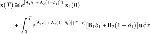
This approximate response of Eq. (35.4) is identical to the exact response obtained from the nonlinear continuous time-invariant state-space model (35.7), supposing that the average values of x, denoted ˉx![]() , are the new state variables and considering δ2=1−δ1. Moreover, if A1 A2=A2 A1, the approximation is exact:
, are the new state variables and considering δ2=1−δ1. Moreover, if A1 A2=A2 A1, the approximation is exact:
˙ˉx=[A1δ1+A2δ2]ˉx+[B1δ1+B2δ2]ˉuˉy=[C1δ1+C2δ2]ˉx+[D1δ1+D2δ2]ˉu
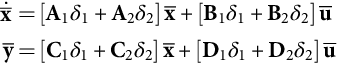
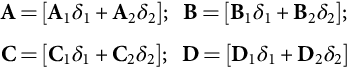
For λmaxT≪1, the model (35.7), often referred to as the state-space averaged model, is also said to be obtained by “averaging” Eq. (35.4) over one period, under small ripple and slow variations, as the average of products is approximated by products of the averages. Comparing Eq. (35.7) with Eq. (35.1), the relations (35.8), defining the state-space averaged model, are obtained:
A=[A1δ1+A2δ2];B=[B1δ1+B2δ2];C=[C1δ1+C2δ2];D=[D1δ1+D2δ2]
Example 35.1
State-space models for the buck–boost dc/dc converter
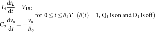
Consider the simplified circuitry of the buck-boost converter of Fig. 35.1 switching at fs=20 kHz (T=50 μs) with VDCmax=28 V, VDCmin=22 V, Vo=24 V, Li=400 μH, Co=2700 μF, and Ro=2 Ω.
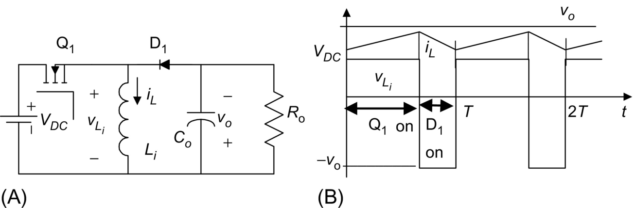
The differential equations governing the dynamics of the state vector x=[iL, vo]T (T denotes the transpose of vectors or matrices) are
LidiLdt=VDCCodvodt=−voRofor0≤t≤δ1T(δ(t)=1,Q1isonandD1isoff)
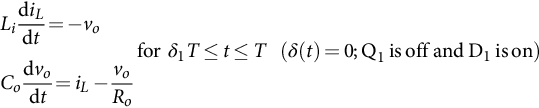
LidiLdt=−voCodvodt=iL−voRoforδ1T≤t≤T(δ(t)=0;Q1isoffandD1ison)
Comparing Eqs. (35.9) and (35.10) with Eqs. (35.2) and (35.3) and considering y=[vo, iL]T, the following matrices can be identified:
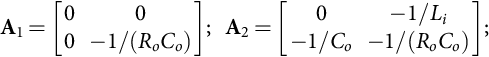
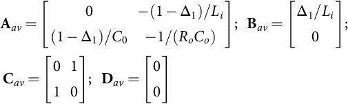
A1=[000−1/(RoCo)];A2=[0−1/Li−1/Co−1/(RoCo)];
B1=[1/Li,0]T;B2=[0,0]T;u=[VDC];
C1=[0110];C2=[0110];

D1=[0,0]T;D2=[0,0]T
From Eqs. (35.4) and (35.5), the switched state-space model of this switching converter is
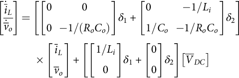
[˙iL˙vo]=[0−(1−δ(t))/Li(1−δ(t))/Co−1/(RoCo)][iLvo]+[δ(t)/Li0]VDC[voiL]=[0110][iLvo]+[00][VDC]

Now, applying Eq. (35.7), Eqs. (35.12) and (35.13) can be obtained:
[˙ˉiL˙ˉvo]=[[000−1/(RoCo)]δ1+[0−1/Li1/Co−1/RoCo]δ2]×[ˉiLˉvo]+[[1/Li0]δ1+[00]δ2][ˉVDC]
[ˉvoˉiL]=[[0110]δ1+[0110]δ2][ˉiLˉvo]+[[00]δ1+[00]δ2][ˉVDC]

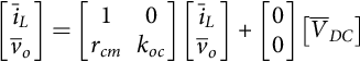
From Eqs. (35.12) and (35.13), the state-space averaged model, written as a function of δ1, is
[˙ˉiL˙ˉvo]=[0−(1−δ1)/Li(1−δ1)/Co−1/(RoCo)][ˉiLˉvo]+[δ1/Li0][ˉVDC]
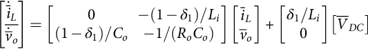
[ˉvoˉiL]=[0110][ˉiLˉvo]+[00][ˉVDC]

The eigenvalues sbb1,2![]() or characteristic roots of A are the roots of |sI−A|. Therefore,
or characteristic roots of A are the roots of |sI−A|. Therefore,
sbb1,2=−12RoCo±√14(RoCo)2−(1−δ1)2LiCo
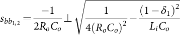
Since λmax is the maximum of the absolute values of all the eigenvalues of A, the model (35.14) and (35.15) is valid for switching frequencies fs (fs=1/T) that verify λmaxT≪1. Therefore, as T≪1/λmax, the values of T that approximately verify this restriction are T≪1/max(|sbb1,2|). Given these buck-boost converter data, T≪2 ms is obtained. Therefore, the converter switching frequency must obey fs≫max(|sbb1,2|), implying switching frequencies above, say, 5 kHz. Consequently, the buck-boost switching frequency, the inductor value, and the capacitor value were chosen accordingly.
This restriction can be further used to discuss the maximum frequency ωmax for which the state-space averaged model is still valid, given a certain switching frequency. As λmax can be regarded as a frequency, the preceding constraint brings ωmax≪2πfs, say ωmax<2πfs/10, which means that the state-space averaged model is a good approximation at frequencies under one-tenth of the power converter switching frequency.
The state-space averaged model (35.14) and (35.15) is also the state-space model of the circuit represented in Fig. 35.2. Hence, this circuit is often named “the averaged equivalent circuit” of the buck-boost converter and allows the determination, under small ripple and slow variations, of the average equivalent circuit of the converter switching cell (power transistor plus diode).

The average equivalent circuit of the switching cell (Fig. 35.3A) is represented in Fig. 35.3B and emerges directly from the state-space averaged model (35.14) and (35.15). This equivalent circuit can be viewed as the model of an “ideal transformer” (Fig. 35.3C), whose primary to secondary ratio (v1/v2) can be calculated applying Kirchhoff's voltage law to obtain−v1+vs−v2=0. As v2=δ1vs, it follows that v1=vs(1−δ1), giving (v1/v2)=(1−δ1)/δ1. The same ratio could be obtained beginning with iL=i1+i2 and i1=δ1iL (Fig. 35.3B), which gives i2=iL(1−δ1) and (i2/i1)=δ2/δ1.

The average equivalent circuit concept, obtained from Eq. (35.7) or Eqs. (35.14) and (35.15), can be applied to other switching converters, with or without a similar switching cell, to obtain transfer functions or to simulate the converter average behavior. The average equivalent circuit of the switching cell can be applied to converters with the same switching cell operating in the continuous conduction mode. However, note that the state variables of Eq. (35.7) or Eqs. (35.14) and (35.15) are the mean values of the converter instantaneous variables and, therefore, do not represent their ripple components. The inputs of the state-space averaged model are the mean values of the converter inputs over one switching period.
35.2.2.3 Linearized State-Space Averaged Model
The converter outputs ˉy![]() must be regulated actuating on the duty cycle δ(t), and the converter inputs ū usually present perturbations due to the load and power supply variations. State variables are decomposed in small ac perturbations (denoted by “~”) and dc steady-state quantities (represented by uppercase letters). Therefore,
must be regulated actuating on the duty cycle δ(t), and the converter inputs ū usually present perturbations due to the load and power supply variations. State variables are decomposed in small ac perturbations (denoted by “~”) and dc steady-state quantities (represented by uppercase letters). Therefore,
ˉx=X+˜xˉy=Y+˜yˉu=U+˜uδ1=Δ1+˜δδ2=Δ2−˜δ

Using Eq. (35.17) in Eq. (35.7) and rearranging terms, it is obtained:
˙˜x=[A1Δ1+A2Δ2]X+[B1Δ1+B2Δ2]U+[A1Δ1+A2Δ2]˜x+[(A1−A2)X+(B1−B2)U]˜δ+[B1Δ1+B2Δ2]˜u+[(A1−A2)]˜x+(B1−B2)˜u]˜δ
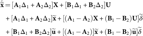
Y+˜y=[C1Δ1+C2Δ2]X+[D1Δ1+D2Δ2]U+[C1Δ1+C2Δ2]˜x+[(C1−C2)X+(D1−D2)U]˜δ+[D1Δ1+D2Δ2]˜u+[(C1−C2)]˜x+(D1−D2)˜u]˜δ

The terms [A1Δ1+A2 Δ2] X + [B1 Δ1+B2 Δ2] U and [C1 Δ1+C2 Δ2] X + [D1 Δ1+D2 Δ2] U, respectively, from Eqs. (35.18) and (35.19) represent the steady-state behavior of the system. As in steady-state ˙X=0![]() , the following relationships hold:
, the following relationships hold:
0=[A1,Δ1,+,A2,Δ2]X+[B1,Δ1,+,B2,Δ2]U
Y=[C1,Δ1,+,C2,Δ2]X+[D1,Δ1,+,D2,Δ2]U
Neglecting higher-order terms ([(A1−A2)˜x+(B1−B2)˜u)]˜δ≈0![]() of Eqs. (35.18) and (35.19), the linearized small-signal state-space averaged model is
of Eqs. (35.18) and (35.19), the linearized small-signal state-space averaged model is
˙˜x=[A1Δ1+A2Δ2]˜x+[(A1−A2)X+(B1−B2)U]˜δ+[B1Δ1+B2Δ2]˜u˜y=[C1Δ1+C2Δ2]˜x+[(C1−C2)X+(D1−D2)U]˜δ+[D1Δ1+D2Δ2]˜u

or
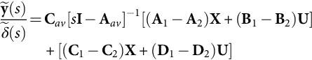
˙˜x=Aav˜x+Bav˜u+[(A1−A2)X+(B1−B2)U]˜δ˜y=Cav˜x+Dav˜u+[(C1−C2)X+(D1−D2)U]˜δ

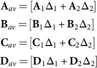
with
Aav=[A1Δ1+A2Δ2]Bav=[B1Δ1+B2Δ2]Cav=[C1Δ1+C2Δ2]Dav=[D1Δ1+D2Δ2]
35.2.3 Converter Transfer Functions
Using Eq. (35.20) in Eq. (35.21), the input U to output Y steady-state relations (35.25), needed for open-loop and feedforward control, can be obtained:
YU=−CavA−1avBav+Dav

Applying Laplace transforms to Eq. (35.23) with zero initial conditions and using the superposition theorem, the small-signal duty-cycle ˜δ![]() -to-output ỹ transfer functions (35.26) can be obtained considering zero line perturbations (ũ=0):
-to-output ỹ transfer functions (35.26) can be obtained considering zero line perturbations (ũ=0):
˜y(s)˜δ(s)=Cav[sI−Aav]−1[(A1−A2)X+(B1−B2)U]+[(C1−C2)X+(D1−D2)U]
The line-to-output transfer function (or audio susceptibility transfer function) (35.27) is derived using the same method, considering now zero small-signal duty-cycle perturbations (˜δ=0)![]() :
:
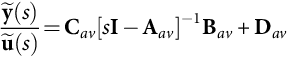
˜y(s)˜u(s)=Cav[sI−Aav]−1Bav+Dav
Example 35.2
Buck–Boost dc/dc converter transfer functions
From Eqs. (35.14) and (35.15) of Example 35.1 and Eq. (35.23), making X=[IL, Vo]T, Y=[Vo, IL]T and U=[VDC], the linearized small-signal state-space model of the buck-boost converter is
[˙˜iL˙˜vo]=[0−(1−Δ1)/Li(1−Δ1)/Co−1/(RoCo)][˜iL˜vo]+[Δ1/Li0][˜vDC]+[0˜δ/Li−˜δ/Co0][ILVo]+[VDC/Li0][˜δ][˜vo˜iL]=[0110][˜iL˜vo]+[00][˜vDC]

From Eqs. (35.24) and (35.28), the following matrices are identified:
Aav=[0−(1−Δ1)/Li(1−Δ1)/C0−1/(RoCo)];Bav=[Δ1/Li0];Cav=[0110];Dav=[00]
The averaged linear equivalent circuit, resulting from Eq. (35.28) or from the linearization of the averaged equivalent circuit (Fig. 35.2) derived from Eqs. (35.14) and (35.15), now includes the small-signal current source ˜δIL![]() in parallel with the current source Δ1ĩL and the small-signal voltage source ˜δ(VDC+Vo)
in parallel with the current source Δ1ĩL and the small-signal voltage source ˜δ(VDC+Vo)![]() in series with the voltage source Δ1(˜vdc+˜vo)
in series with the voltage source Δ1(˜vdc+˜vo)![]() . The supply voltage source ˉVDC
. The supply voltage source ˉVDC![]() is replaced by the voltage source ṽDC.
is replaced by the voltage source ṽDC.
Using Eq. (35.29) in Eq. (35.25), the input U to output Y steady-state relations are
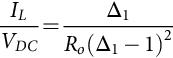
ILVDC=Δ1Ro(Δ1−1)2
VoVDC=Δ11−Δ1
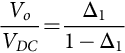
These relations are the well-known steady-state transfer relationships of the buck-boost converter [2,5,6]. For open-loop control of the Vo output, knowing the nominal value of the power supply VDC and the required Vo, the value of Δ1 can be offline calculated from Eq. (35.31) (Δ1=Vo/(Vo+VDC)). A modulator such as that described in Section 35.2.4, with the modulation signal proportional to Δ1, would generate the signal δ(t). The open-loop control for fixed output voltages is possible, if the power supply VDC is almost constant and the converter load does not change significantly. If the VDC value presents disturbances, then the feedforward control can be used, calculating Δ1 online, so that its value will always be in accordance with Eq. (35.31). The correct Vo value will be attained at steady state, despite input voltage variations. However, because of converter parasitic reactances, not modeled here (see Example 35.3), in practice, a steady-state error would appear. Moreover, the transient dynamics imposed by the converter would present overshoots, being often not suited for demanding applications.
From Eq. (35.27), the line-to-output transfer functions are
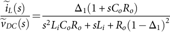
˜iL(s)˜vDC(s)=Δ1(1+sCoRo)s2LiCoRo+sLi+Ro(1−Δ1)2
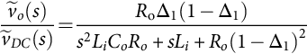
˜vo(s)˜vDC(s)=RoΔ1(1−Δ1)s2LiCoRo+sLi+Ro(1−Δ1)2
From Eq. (35.26), the small-signal duty-cycle ˜δ![]() -to-output ỹ transfer functions are
-to-output ỹ transfer functions are
˜iL(s)˜δ(s)=VDC(1+Δ1+sCoRo)/(1−Δ1)s2LiCoRo+sLi+Ro(1−Δ1)2

˜vo(s)˜δ(s)=VDC(Ro−sLiΔ1)/(1−Δ1)2)s2LiCoRo+sLi+Ro(1−Δ1)2
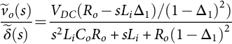
These transfer functions enable the choice and feedback loop design of the compensation network. Note the positive zero in ˜vo(s)/˜δ(s),![]() pointing out a nonminimum-phase system. These equations could also be obtained using the small-signal equivalent circuit derived from Eq. (35.28) or from the linearized model of the switching cell (Fig. 35.3B), substituting the current source δ1īL by the current sources Δ1˜iLand˜δIL
pointing out a nonminimum-phase system. These equations could also be obtained using the small-signal equivalent circuit derived from Eq. (35.28) or from the linearized model of the switching cell (Fig. 35.3B), substituting the current source δ1īL by the current sources Δ1˜iLand˜δIL![]() in parallel and the voltage source δ1ˉvs
in parallel and the voltage source δ1ˉvs![]() by the voltage sources Δ1(˜vDC+˜vo)and˜δ(VDC+Vo)
by the voltage sources Δ1(˜vDC+˜vo)and˜δ(VDC+Vo)![]() in series.
in series.
Example 35.3
Transfer functions of the forward dc/dc converter
Consider the forward (buck-derived) converter of Fig. 35.4 switching at fs=100 kHz (T=10 μs) with VDC=300 V, n=30, Vo=5 V, Li=20 μH, rL=0.01 Ω, Co=2200 μF, rC=0.005 Ω, and Ro=0.1 Ω.
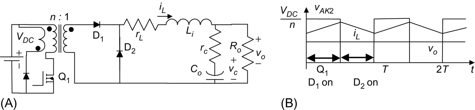
Assuming x=[iL, vC]T, δ(t)=1 when both Q1 and D1 are on and D2 is off (0≤t≤δ1 T), and δ(t)=0 when both Q1 and D1 are off and D2 is on (δ1 T≤t≤T), the switched state-space model of the forward converter, considering as output vector y=[iL, vo]T, is
diLdt=−(RorC+RorL+rLrC)Li(Ro+rC)iL−RoLi(Ro+rC)vc+δ(t)nVDCdvCdt=Ro(Ro+rC)CoiL−1(Ro+rC)CovCvo=rC1+rC/RoiL+11+rC/RovC

Making rcm=rC/(1+rC/Ro), Roc=Ro+rC, koc=Ro/Roc, and rP=rL+rcm and comparing Eq. (35.36) with Eqs. (35.2) and (35.3), the following matrices can be identified:
A1=A2=[−rp/Li−koc/Likoc/Co−1/(RocCo)];
B1=[1/(nLi),0]T;B2=[0,0]T;u=[VDC]
C1=C2=[10rcmkoc];D1=D2=[00]T
Now, applying Eq. (35.7), the exact (since A1=A2) state-space averaged model (35.37) and (35.38) is obtained:
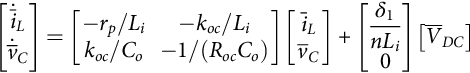
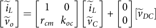
[˙ˉiL˙ˉvC]=[−rp/Li−koc/Likoc/Co−1/(RocCo)][ˉiLˉvC]+[δ1nLi0][ˉVDC]
[ˉiLˉvo]=[10rcmkoc][ˉiLˉvo]+[00][ˉVDC]
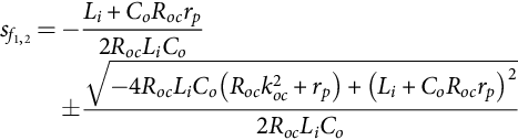
Since A1=A2, this model is valid for ωmax<2πfs. The converter eigenvalues sf1,2![]() are
are
sf1,2=-Li+CoRocrp2RocLiCo±√−4RocLiCo(Rock2oc+rp)+(Li+CoRocrp)22RocLiCo
The equivalent circuit arising from Eqs. (35.37) and (35.38) is represented in Fig. 35.5. It could also be obtained with the concept of the switching cell equivalent circuit Fig. 35.3 of Example (35.1).

Making X=[IL, VC]T, Y=[IL, Vo]T and U=[VDC], from Eq. (35.23), the small-signal state-space averaged model is
[˙˜iL˙˜vC]=[−rp/Li−koc/Likoc/Co−1/(RocCo)][ˉiL˜vC]+[Δ1/(nLi)0][˜vDC]+[VDC/(nLi)0][˜δ]
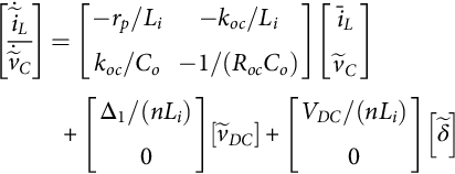
[˜iL˜vo]=[10rcmkoc][˜iL˜vC]+[00][˜vDC]
From Eq. (35.25), the input U to output Y steady-state relations are
ILVDC=Δ1n(k2ocRoc+rp)

VoVDC=Δ1(k2ocRoc+rcm)n(k2ocRoc+rp)
Making rC=0, rL=0, and n=1, the former relations give the well-known dc transfer relationships of the buck dc/dc converter. Relations (35.42) and (35.43) allow the open-loop and feedforward control of the converter, as discussed in Example 35.2, provided that all the modeled parameters are time-invariant and accurate enough.
From Eq. (35.27), the line-to-output transfer functions are derived:
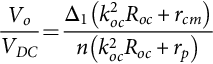
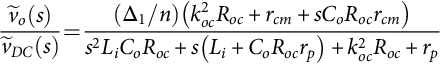
˜iL(s)˜vDC(s)=(Δ1/n)(1+sCoRoc)s2LiCoRoc+s(Li+CoRocrp)+k2ocRoc+rp
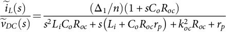
˜vo(s)˜vDC(s)=(Δ1/n)(k2ocRoc+rcm+sCoRocrcm)s2LiCoRoc+s(Li+CoRocrp)+k2ocRoc+rp
Using Eq. (35.26), the small-signal duty-cycle ˜δ![]() -to-output ỹ transfer functions are
-to-output ỹ transfer functions are
˜iL(s)δ(s)=(VDC/n)(1+sCoRoc)s2LiCoRoc+s(Li+CoRocrp)+k2ocRoc+rp
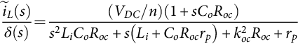
˜vo(s)δ(s)=(VDC/n)(k2ocRoc+rcm+sCoRocrcm)s2LiCoRoc+s(Li+CoRocrp)+k2ocRoc+rp

The real zero of Eq. (35.47) is due to rC, the equivalent series resistance (ESR) of the output capacitor. A similar zero would occur in the buck-boost converter (Example 35.2), if the ESR of the output capacitor had been included in the modeling.
35.2.4 Pulse Width Modulator Transfer Functions
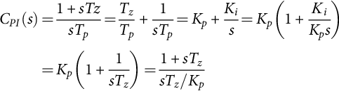
In what is often referred to as the pulse-width-modulation (PWM) voltage-mode control, the output voltage uc(t) of the error (between desired and actual output) amplifier plus regulator, processed if needed, is compared with a repetitive or carrier waveform r(t), to obtain the switching variable δ(t) (Fig. 35.6A). This function controls the power switch, turning it on at the beginning of the period and turning it off when the ramp exceeds the uc(t) voltage. In Fig. 35.6B, the opposite occurs (turnoff at the end of the period and turn-on when the uc(t) voltage exceeds the ramp).
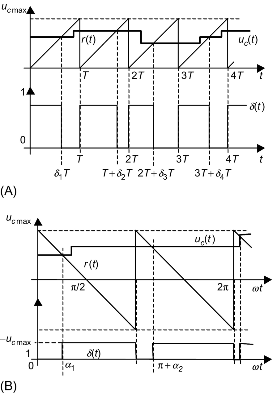
Considering r(t) as represented in Fig. 35.6A (r(t)=ucmaxt/T), δk is obtained equating r(t)=uc giving δk=uc (t)/ucmax or δk/uc (t)=GM (GM =1/ucmax). In Fig. 35.6B, the switching-on angle αk is obtained from r(t)=ucmax−2ucmaxωt/π and uc (t)=ucmax−2ucmax αk/π, giving αk=(π/2)×(1−uc/ucmax) and GM=∂αk/∂uc=−π/(2ucmax).
Since, after turnoff or turn-on, any control action variation of uc(t) will only affect the converter duty cycle in the next period (or sample for digital hardware), a time delay is introduced in the control loop. For simplicity, with small-signal perturbations around the operating point, this delay is assumed almost constant and equal to its mean value (T/2). Then, the transfer function of the PWM modulator is
˜δ(s)˜uc(s)=GMe−sT/2=GMes(T/2)=GM1+sT2+s22!(T2)2+…+sjj!(T2)j+…≈GM1+sT2

The final approximation of Eq. (35.48), valid for ωT/2<√2/2![]() , [7] suggests that the PWM modulator can be considered as an amplifier with gain GM and a dominant pole. Notice that this pole occurs at a frequency doubling the switching frequency, and most state-space averaged models are valid only for frequencies below one-tenth of the switching frequency. Therefore, in most situations, this modulator pole can be neglected, being simply δ(s)=GMuc(s), as the dominant pole of Eq. (35.48) stays at least one decade to the left of the dominant poles of the converter.
, [7] suggests that the PWM modulator can be considered as an amplifier with gain GM and a dominant pole. Notice that this pole occurs at a frequency doubling the switching frequency, and most state-space averaged models are valid only for frequencies below one-tenth of the switching frequency. Therefore, in most situations, this modulator pole can be neglected, being simply δ(s)=GMuc(s), as the dominant pole of Eq. (35.48) stays at least one decade to the left of the dominant poles of the converter.
35.2.5 Linear Feedback Design Ensuring Stability
In the application of classical linear feedback control to switching power converters, Bode plots and root locus are, usually, suitable methods to assess system performance and stability. General rules for the design of the compensated open-loop transfer function are as follows:
The low-frequency gain should be high enough to minimize output steady-state errors.
The frequency of 0 dB gain (unity gain), ω0dB, should be placed close to the maximum allowed by the modeling approximations (λmaxT≪1), to allow fast response to transients. In practice, this frequency should be almost an order of magnitude lower than the switching frequency.
To ensure stability, the phase margin, defined as the additional phase shift needed to render the system unstable without gain changes (or the difference between the open-loop system phase at ω0dB and −180°), must be positive and in general greater than 30° (45−70° is desirable). In the root locus, no poles should enter the right half of the complex plane.
To increase stability, the gain should be less than −30 dB at the frequency where the phase reaches −180° (gain margin greater than 30 dB).
Transient behavior and stability margins are related: The obtained damping factor is generally 0.01 times the phase margin (in degrees), and overshoot (in percent) is given approximately by 75° minus the phase margin. The product of the rise time (in seconds) and the closed-loop bandwidth (in rad/s) is close to 2.8.
To guarantee gain and phase margins, the following series compensation transfer functions (usually implemented with operational amplifiers) are often used [8]:
35.2.5.1 Types of Compensation
Lag and lead compensation
Lag compensation should be used in converters with good stability margin but poor steady-state accuracy. If the frequencies 1/Tp and 1/Tz of Eq. (35.49) with 1/Tp<1/Tz are chosen sufficiently below the unity gain frequency, lag-lead compensation lowers the loop gain at high frequency but maintains the phase unchanged for frequencies f≫1/Tz. Then, the dc gain can be increased to reduce the steady-state error without significantly decreasing the phase margin:
CLL(s)=kLL1+sTz1+sTp=kLLTzTps+1/Tzs+1/Tp

Lead compensation can be used in converters with good steady-state accuracy but poor stability margin. If the frequencies 1/Tp and 1/Tz of Eq. (35.49) with 1/Tp>1/Tz are chosen below the unity gain frequency, lead-lag compensation increases the phase margin without significantly affecting the steady-state error. The Tp and Tz values are chosen to increase the phase margin, fastening the transient response and increasing the bandwidth.
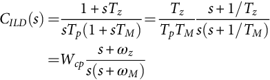
Proportional–Integral compensation
Proportional-integral (PI) compensators (35.50) are used to guarantee null steady-state error with acceptable rise times. The PI compensators are a particular case of lag-lead compensators, therefore suitable for converters with good stability margin but poor steady-state accuracy:
CPI(s)=1+sTzsTp=TzTp+1sTp=Kp+Kis=Kp(1+ΚiKps)=Kp(1+1sTz)=1+sTzsTz/Kp
Proportional–integral plus high-frequency pole compensation
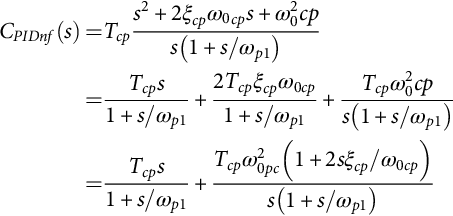
This integral plus zero-pole compensation (35.51) combines the advantages of a PI with lead or lag compensation. It can be used in converters with good stability margin but poor steady-state accuracy. If the frequencies 1/TM and 1/Tz (1/Tz<1/TM) are carefully chosen, compensation lowers the loop gain at high frequency while only slightly lowering the phase to achieve the desired phase margin:
CILD(s)=1+sTzsTp(1+sTM)=TzTpTMs+1/Tzs(s+1/TM)=Wcps+ωzs(s+ωM)
Proportional-integral derivative (PID), plus high-frequency poles
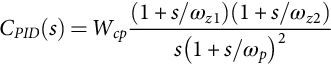
The PID notch filter type (35.52) scheme is used in converters with two lightly damped complex poles, to increase the response speed, while ensuring zero steady-state error. In most switching power converters, the two complex zeros are selected to have a damping factor greater than the converter complex poles and slightly smaller oscillating frequency. The high-frequency pole is placed to achieve the needed phase margin [9]. The design is correct if the complex pole loci, heading to the complex zeros in the system root locus, never enter the right half plane:
CPIDnf(s)=Tcps2+2ξcpω0cps+ω20cps(1+s/ωp1)=Tcps1+s/ωp1+2Tcpξcpω0cp1+s/ωp1+Tcpω20cps(1+s/ωp1)=Tcps1+s/ωp1+Tcpω20pc(1+2sξcp/ω0cp)s(1+s/ωp1)
For systems with a high-frequency zero placed at least one decade above the two lightly damped complex poles, the compensator (35.53), with ωz1≈ωz2<ωp, can be used. Usually, the two real zeros present frequencies slightly lower than the frequency of the converter complex poles. The two high-frequency poles are placed to obtain the desired phase margin [9]. The obtained overall performance will often be inferior to that of the PID type notch filter:
CPID(s)=Wcp(1+s/ωz1)(1+s/ωz2)s(1+s/ωp)2
35.2.5.2 Compensator Selection and Design
The procedure to select the compensator and to design its parameters can be outlined as follows:
1. Compensator selection: In general, since VDC perturbations exist, null steady-state error guarantee is needed. High-frequency poles are usually necessary, if the transfer function shows a −6 dB/octave roll-off due to high-frequency left plane zeros. Therefore, in general, two types of compensation schemes with integral action (35.51) or (35.50) and (35.52) or (35.53) can be tried. Compensator (35.52) is usually convenient for systems with lightly damped complex poles.
2. Unity gain frequency ω0dB choice:
• If the selected compensator has no complex zeros, it is better to be conservative, choosing ω0dB sufficiently below the frequency of the lightly damped poles of the converter (or the frequency of the right half-plane zeros if lower). However, because of the resonant peak of most converter transfer functions, the phase margin can be obtained at a frequency near the resonance. If the phase margin is not enough, the compensator gain must be lowered.
• If the selected compensator has complex zeros, ω0dB can be chosen slightly above the frequency of the lightly damped poles.
3. Desired phase margin (φM) specification φM≥30° (preferably between 45 and 70°).
4. Compensator zero-pole placement to achieve the desired phase margin:
• With the integral plus zero-pole compensation type (35.51), the compensator phase φcp, at the maximum frequency of unity gain (often ω0dB), equals the phase margin (φM) minus 180° and minus the converter phase φcv,(φcp=φM−180°−φcv). The zero-pole position can be obtained calculating the factor fct=tg (π/2+ φcp/2) being ωz=ω0dB/fct and ωM=ω0dBfct.
• With the PID notch filter type (35.52) controller, the two complex zeros are placed to have a damping factor ξp roughly equal to two times the damping ξz of the converter complex poles and oscillating frequency ω0cp 30% smaller than the complex poles frequency ωp. The high-frequency pole ωp1 is placed to achieve the needed phase margin (ωp1≈(ω0cp·ω0dB)1/2fct2 with fct=tg (π/2+φcp/2) and φcp=φM−180°−φcv [5]). Alternatively, since for stability ξz ω0cp>ξp ωp and ωp√1−ξ2p>ω0cp√1−ξ2z![]() , it is obtained 1>ξz>ξp and using the geometric mean, ω0cp=ωp√ξpξz√1−ξ2p1−ξ2z
, it is obtained 1>ξz>ξp and using the geometric mean, ω0cp=ωp√ξpξz√1−ξ2p1−ξ2z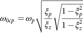 .
.
5. Compensator gain calculation (the product of the converter and compensator gains at the ω0dB frequency must be one).
6. Stability margin verification using Bode plots and root locus.
7. Result evaluation. Restarting the compensator selection and design, if the attained results are still not good enough.
Note that several modern computer programs, such as MATLAB, provide very easy and efficient tools (such as SISOTOOL) to design these controllers, even considering that switching power converters are discrete systems. Optimum controllers such as linear-quadratic-Gaussian (LQG, LQR) controllers, whose performances might be much better than linear controllers, can also be designed using the same tools. However, in evaluating optimum controller results, care must be taken in order to guarantee that the controlled converter frequency bandwidth and gain are not beyond the validity limits of the used models.
35.2.6 Examples: Buck–Boost DC/DC Converter, Forward DC/DC Converter, 12 Pulse Rectifiers, Buck–Boost DC/DC Converter in the Discontinuous Mode (Voltage and Current Mode), Three-phase PWM Inverters
Example 35.4
Feedback design for the buck–boost dc/dc converter
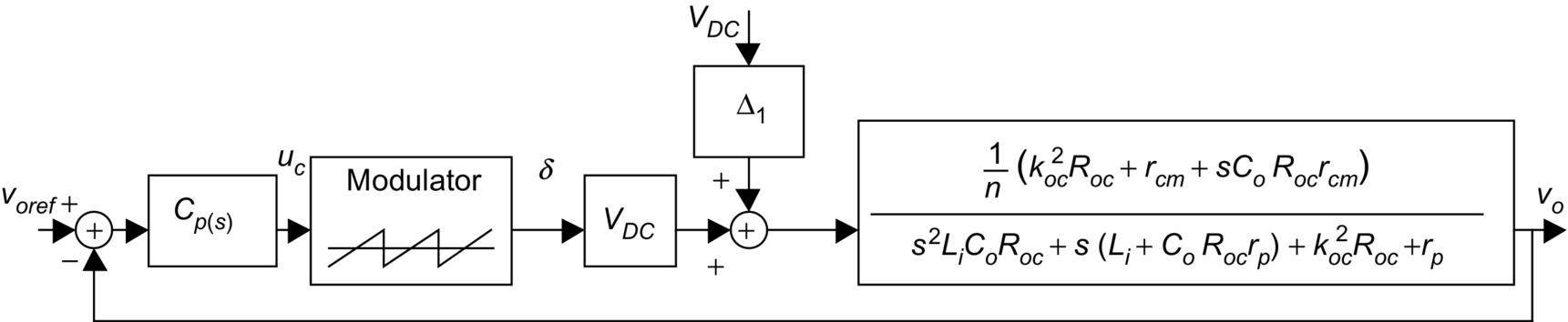
Consider the converter output voltage vo (Fig. 35.1) to be the controlled output. From Example 35.2 and Eqs. (35.33) and (35.35), the block diagram of Fig. 35.7 is obtained. The modulator transfer function is considered a pure gain (GM=0.1). The magnitude and phase of the open-loop transfer function vo/uc (Fig. 35.8A trace 1) shows a resonant peak due to the two lightly damped complex poles and the associated −12 dB/octave roll-off. The right half-plane zero changes the roll-off to −6 dB/octave and adds −90° to the converter phase (nonminimum-phase converter).
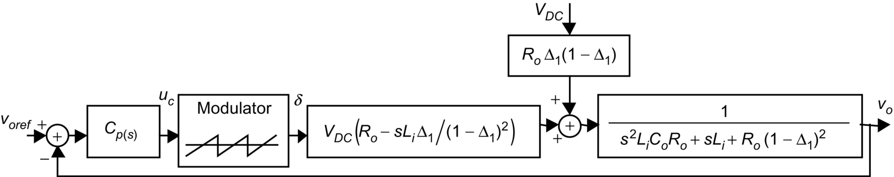
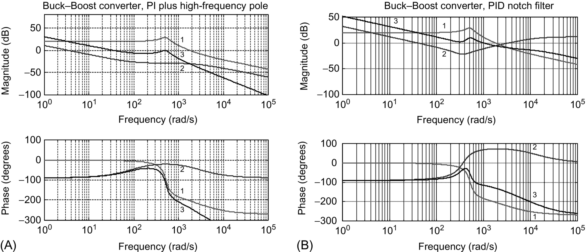
Compensator selection. As VDC perturbations exist, null steady-state error guarantee is needed. High-frequency poles are needed given the −6 dB/octave final slope of the transfer function. Therefore, two compensation schemes (35.51) and (35.52) with integral action are tried here. The buck-boost converter controlled with integral plus zero-pole compensation presents, in closed-loop, two complex poles closer to the imaginary axes than in open loop. These poles should not dominate the converter dynamics. Instead, the real pole resulting from the open-loop pole placed at the origin should be almost the dominant one, thus slightly lowering the calculated compensator gain. If the ω0dB frequency is chosen too low, the integral plus zero-pole compensation turns into a pure integral compensator (ωz=ωM=ω0dB). However, the obtained gains are too low, leading to very slow transient responses.
Results showing the transient responses to voref and VDC step changes, using the selected compensators and converter Bode plots (Fig. 35.8), are shown (Fig. 35.9). The compensated real converter transient behavior occurs in the buck and in the boost regions. Notice the nonminimum-phase behavior of the converter (mainly in Fig. 35.9B), the superior performance of the PID notch filter compensator, and the unacceptable behavior of the PI with high-frequency pole. Care should be taken with load changes, when using this compensator, since instability can easily occur.
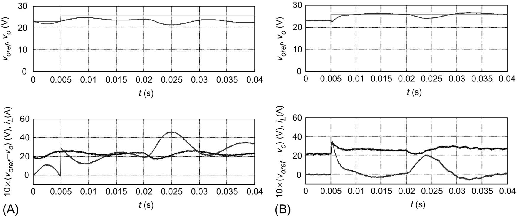
The compensator critical values, obtained with the root-locus studies, are Wcpcrit=700 s−1 for the integral plus zero-pole compensator, Tcpcrit=0.0012 s for the PID notch filter, and WIcpcrit=18 s−1 for the integral compensation derived from the integral plus zero-pole compensator (ωz=ωM). This confirms the Bode-plot design and allows stability estimation with changing loads and power supply.
Example 35.5
Feedback design for the forward dc/dc converter
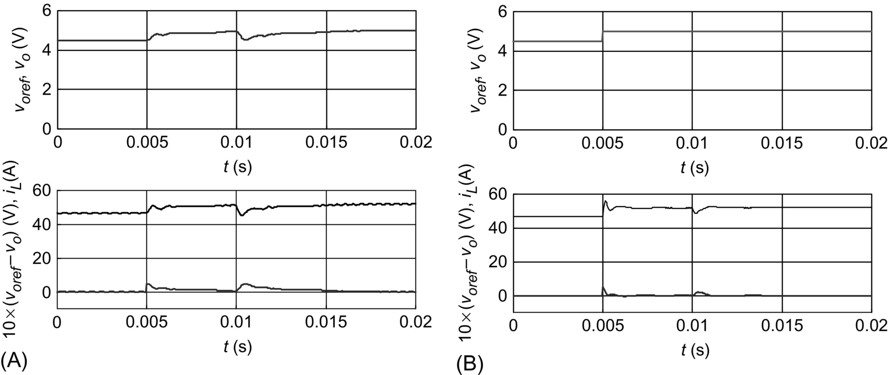
Consider the output voltage vo of the forward converter (Fig. 35.4A) to be the controlled output. From Example 35.3 and Eqs. (35.45) and (35.47), the block diagram of Fig. 35.10 is obtained. As in Example 35.4, the modulator transfer function is considered as a pure gain (GM=0.1). The magnitude and phase of the open-loop transfer function vo/uc (Fig. 35.11A trace 1) shows an open-loop stable system. Since integral action is needed to have some disturbance rejection of the voltage source VDC, the compensation schemes used in Example 35.4, obtained using the same procedure (Fig. 35.11), were also tested.
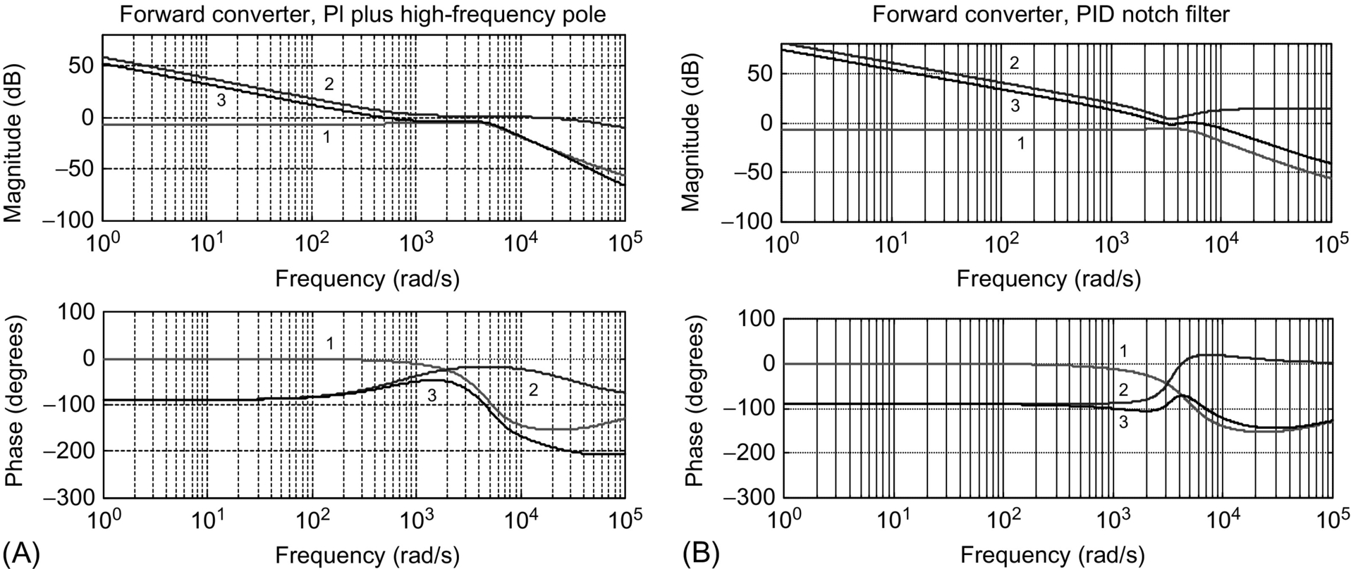
Results, showing the transient responses to voref and VDC step changes, are shown (Fig. 35.12). Both compensators (35.51) and (35.52) are easier to design than the ones for the buck-boost converter, and both have acceptable performances. Moreover, the PID notch filter presents a much faster response.
Alternatively, a PID feedback controller such as Eq. (35.53) can be easily hand-adjusted, starting with the proportional, integral, and derivative gains all set to zero. In the first step, the proportional gain is increased until the output presents an oscillatory response with nearly 50% overshoot. Next, the derivative gain is slowly increased until the overshoot is eliminated. Finally, the integral gain is increased to eliminate the steady-state error as quickly as possible.
Example 35.6
Feedback design for phase controlled rectifiers in the continuous mode
Phase-controlled, p pulse (p>1), thyristor rectifiers (Fig. 35.13A), operating in the continuous mode, present an output voltage with p identical segments within the mains period T. Given this cyclic waveform, the A, B, C, and D matrices for all these p intervals can be written with the same form, in spite of the topological variation. Hence, the state-space averaged model is obtained simply by averaging all the variables within the period T/p. Assuming small variations, the mean value of the rectifier output voltage UDC can be written as [4]:

UDC=Uppπsin(πp)cosα
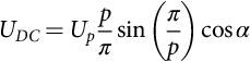
where α is the triggering angle of the thyristors and Up the maximum peak value of the rectifier output voltage, determined by the rectifier topology and the ac supply voltage. The α value can be obtained (α=(π/2)×(1−uc/ucmax)) using the modulator of Fig. 35.6B, where ω=2π/T is the mains frequency. From Eq. (35.54), the incremental gain KR of the modulator plus rectifier yields
KR=∂UDC∂uc=Upp2ucmaxsin(πp)cos(πuc2ucmax)

For a given rectifier, this gain depends on uc and should be calculated for a certain quiescent point. However, for feedback design purposes, keeping in mind that the rectifier could be required to be stable in all operating points, the maximum value of KR, denoted KRM, can be used:
KRM=Upp2ucmaxsin(πp)
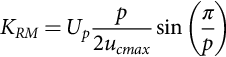
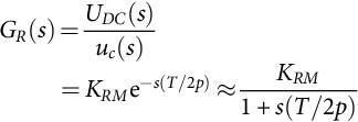
The operation of the modulator, coupled to the rectifier thyristors, introduces a nonnegligible time delay, with mean value T/2p. Therefore, from Eq. (35.48), the modulator-rectifier transfer function GR(s) is
GR(s)=UDC(s)uc(s)=KRMe−s(T/2p)≈KRM1+s(T/2p)
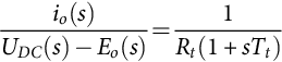
Considering zero Up perturbations, the rectifier equivalent averaged circuit (Fig. 35.13B) includes the loss-free rectifier output resistance Ri, due to the overlap in the commutation phenomenon caused by the mains inductance. Usually, Ri≈pωl/π where l is the equivalent inductance of the lines paralleled during the overlap, half of the line inductance for most rectifiers, except for single-phase bridge rectifiers where l is the line inductance. Here, Lo is the smoothing reactor, and Rm, Lm, and Eo are, respectively, the armature internal resistance, inductance, and back electromotive force of a separately excited dc motor (typical load). Assuming the mean value of the output current as the controlled output, making Lt=Lo+Lm, Rt=Ri+Rm, and Tt=Lt/Rt, and applying Laplace transforms to the differential equation obtained from the circuit of Fig. 35.13B, the output current transfer function is
io(s)UDC(s)−Eo(s)=1Rt(1+sTt)
The rectifier and load are now represented by a perturbed (Eo) second-order system (Fig. 35.14). To achieve zero steady-state error, which ensures steady-state insensitivity to the perturbations, and to obtain closed-loop second-order dynamics, a PI controller (35.50) was selected for Cp(s) (Fig. 35.14). Canceling the load pole (−1/Tt) with the PI zero (−1/Tz) yields

Tz=Lt/Rt
The rectifier closed-loop transfer function io(s)/ioref (s), with zero Eo perturbations, is
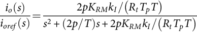
io(s)ioref(s)=2pKRMkI/(RtTpT)s2+(2p/T)s+2pKRMkI/(RtTpT)
The final value theorem enables the verification of the zero steady-state error. Comparing the denominator of Eq. (35.60) with the second-order polynomial s2+2ςωns+ω2n![]() yields
yields
ω2n=2pKRMkI/(RtTpT)4ζ2ω2n=(2p/T)2

Since only one degree of freedom is available (Tp), the damping factor ζ is imposed. Usually, ζ=√2/2![]() is selected, since it often gives the best compromise between response speed and overshoot. Therefore, from Eq. (35.61), Eq. (35.62) arises:
is selected, since it often gives the best compromise between response speed and overshoot. Therefore, from Eq. (35.61), Eq. (35.62) arises:
Tp=4ζ2KRMkIT/(2pRt)=KRMkIT/(pRt)
Note that both Tz (35.59) and Tp (35.62) are dependent upon circuit parameters. They will have the correct values only for dc motors with parameters closed to the nominal load value. Using Eq. (35.62) in Eq. (35.60) yields Eq. (35.63), the second-order closed-loop transfer function of the rectifier, showing that, with loads close to the nominal value, the rectifier dynamics depend only on the mean delay time T/2p:
io(s)ioref(s)=12(T/2p)2s2+sT/p+1
From Eq. (35.63), ωn=√2p/T![]() results, which is the maximum frequency allowed by ωT/2p<√2/2
results, which is the maximum frequency allowed by ωT/2p<√2/2![]() , the validity limit of Eq. (35.48). This implies that ζ≥√2/2
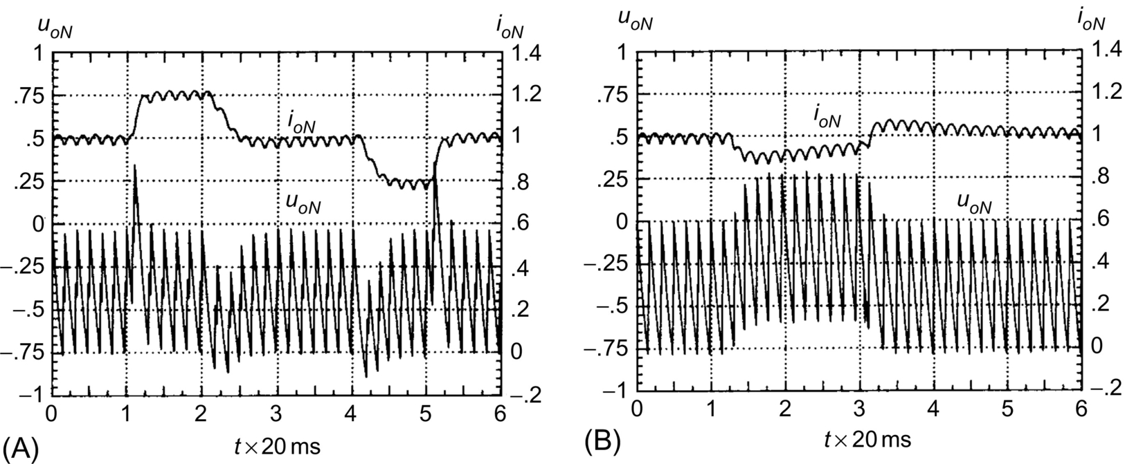
, the validity limit of Eq. (35.48). This implies that ζ≥√2/2![]() , which confirms the preceding choice. For Up=300 V, p=6, T=20 ms, l=0.8 mH, Rm=0.5 Ω, Lt=50 mH, Eo=−150 V, ucmax=10 V, and kI=0.1, Fig. 35.15A shows the rectifier output voltage uoN (uoN=uo/Up) and the step response of the output current ioN (ioN=io/40) in accordance with Eq. (35.63). Notice that the rectifier is operating in the inverter mode. Fig. 35.15B shows the effect, in the io current, of a 50% reduction in the Eo value. The output current is initially disturbed, but the error vanishes rapidly with time.
, which confirms the preceding choice. For Up=300 V, p=6, T=20 ms, l=0.8 mH, Rm=0.5 Ω, Lt=50 mH, Eo=−150 V, ucmax=10 V, and kI=0.1, Fig. 35.15A shows the rectifier output voltage uoN (uoN=uo/Up) and the step response of the output current ioN (ioN=io/40) in accordance with Eq. (35.63). Notice that the rectifier is operating in the inverter mode. Fig. 35.15B shows the effect, in the io current, of a 50% reduction in the Eo value. The output current is initially disturbed, but the error vanishes rapidly with time.
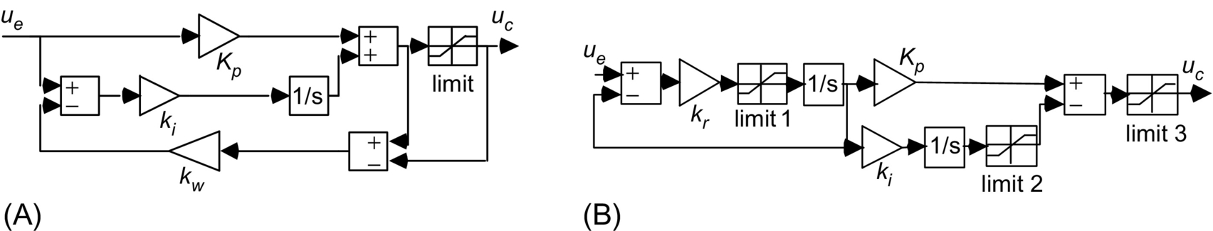
These modeling and compensator design are valid for small perturbations. For large perturbations, the rectifier firing angles will either saturate at the zero value or originate large current overshoots. For large signals, antiwindup schemes (Fig. 35.16A) or error ramp limiters (or soft starters) and limiters of the PI integral component (Fig. 35.16B) must be used. These solutions will also work with other switching power converters.
To use this rectifier current controller as the inner control loop of a cascaded controller for the dc motor speed regulation, a useful first-order approximation of Eq. (35.63) is io(s)/ioref(s)≈1/(sT/p+1).
Although allowing a straightforward compensator selection and precise calculation of its parameters, the rectifier modeling presented here is not suited for stability studies. The rectifier root locus will contain two complex conjugate poles in branches parallel to the imaginary axis. To study the current controller stability, at least the second-order term of Eq. (35.48) in Eq. (35.57) is needed. Alternative ways include the first-order Padé approximation of e−sT/2p, e−sT/2p≈(1−sT/4p)/(1+sT/4p), or the second-order approximation, e−sT/2p≈(1−sT/4p+(sT/2p)2/12)/(1+sT/4p+(sT/2p)2/12). These approaches introduce zeros in the right half-plane (nonminimum-phase systems) and/or extra poles, giving more realistic results. Taking a first-order approximation and root-locus techniques, it is found that the rectifier is stable for Tp>KRM kI T/(4pRt) (ζ>0.25). Another approach uses the conditions of magnitude and angle of the delay function e−sT/2p to obtain the system root locus. Also, the switching power converter can be considered as a sampled data system, at frequency p/T, and Z transform can be used to determine the critical gain and first frequency of instability p/(2 T), usually half the switching frequency of the rectifier.
Example 35.7
Buck–Boost dc/dc converter feedback design in the discontinuous mode
The methodologies just described do not apply to switching power converters operating in the discontinuous mode. However, the derived equivalent averaged circuit approach can be used, calculating the mean value of the discontinuous current supplied to the load, to obtain the equivalent circuit. Consider the buck-boost converter of Example 35.1 (Fig. 35.1) with the new values Li=40 μH, Co=1000 μF, and Ro=15 Ω. The mean value of the current iLo, supplied to the output capacitor and resistor of the circuit operating in the discontinuous mode, can be calculated noting that, if the input VDC and output vo voltages are essentially constant (low ripple), the inductor current rises linearly from zero, peaking at IP=(VDC/Li)δ1 T (Fig. 35.17A). As the mean value of iLo, supposed linear, is ILo=(IPδ2T)/(2 T), using the steady-state input-output relation VDCδ1=Voδ2 and the above IP value, ILo can be written as
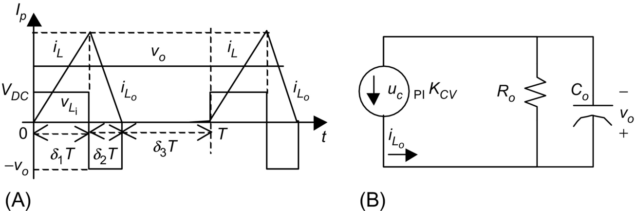
ILo=δ21V2DCT2LiVo

This is a nonlinear relation that could be linearized around an operating point. However, switching power converters in the discontinuous mode seldom operate just around an operating point. Therefore, using a quadratic modulator (Fig. 35.18), obtained integrating the ramp r(t) (Fig. 35.6A) and comparing the quadratic curve to the term ucPIvo/VDC2 (which is easily implemented using the Unitrode UC3854 integrated circuit), the duty cycle δ1 is δ1=√ucPIVo/(ucmaxV2DC)![]() , and a constant incremental factor KCV can be obtained:
, and a constant incremental factor KCV can be obtained:
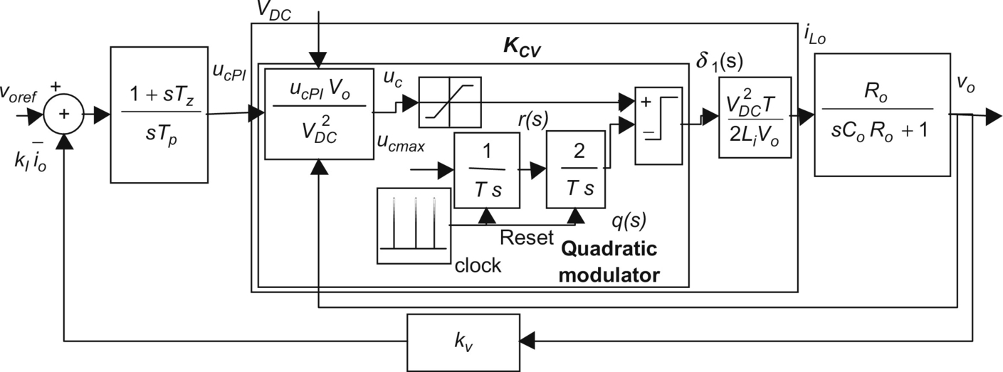
KCV=∂ILo∂ucPI=T2ucmaxLi

Considering zero-voltage perturbations and neglecting the modulator delay, the equivalent averaged circuit (Fig. 35.17B) can be used to derive the output voltage to input current transfer function vo(s)/iLo(s)=Ro/(sCoRo+1). Using a PI controller (35.50), the closed-loop transfer function is
vo(s)voref(s)=KCV(1+sTz)/(CoTp)s2+s(Tp+TzKCVkvRo)/(CoRoTp)+KCVkV/(CoTp)

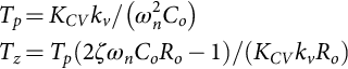
Since two degrees of freedom exist, the PI constants are derived imposing ζ and ωn for the second-order denominator of Eq. (35.66), usually ζ≥√2/2![]() and ωn≤2πfs/10. Therefore,
and ωn≤2πfs/10. Therefore,
Tp=KCVkv/(ω2nCo)Tz=Tp(2ζωnCoRo−1)/(KCVkvRo)
The transient behavior of this converter, with ζ=1 and ωn≈πfs/10, is shown in Fig. 35.19A. Compared with Example 35.2, the operation in the discontinuous conduction mode reduces, by 1, the order of the state-space averaged model and eliminates the zero in the right half of the complex plane. The inductor current does not behave as a true state variable, since during the interval δ3T this current is zero, and this value is always the iLo current initial condition. Given the differences between these two examples, care should be taken to avoid the operation in the continuous mode of converters designed and compensated for the discontinuous mode. This can happen during turn-on or step load changes, and if not prevented, the feedback design should guarantee stability in both modes (Example 35.8 and Fig. 35.20).

Example 35.8
Feedback design for the buck–boost dc/dc converter operating in the discontinuous mode and using current-mode control
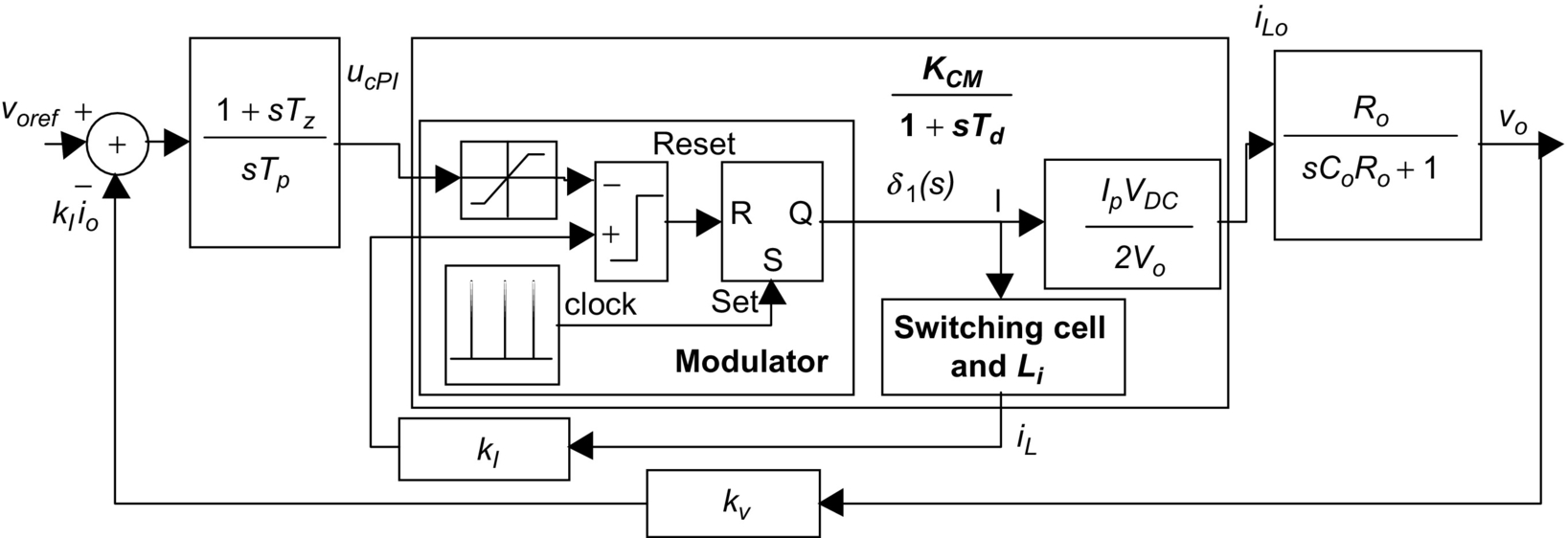
The performances of the buck-boost converter operating in the discontinuous mode can be greatly enhanced if a current-mode control scheme is used, instead of the voltage-mode controller designed in Example 35.7. Current-mode control in switching power converters is the simplest form of state feedback. Current mode needs the measurement of the current iL (Fig. 35.1) but greatly simplifies the modulator design (compare Fig. 35.18 with Fig. 35.20), since no modulator linearization is used. The measured value, proportional to the current iL, is compared with the value ucPI given by the output voltage controller (Fig. 35.20). The modulator switches off the power semiconductor when kIIP=ucPI.
Expressed as a function of the peak iL current IP, ILo becomes (Example 35.7) ILo=IPδ1VDC/(2Vo), or considering the modulator task ILo=ucPIδ1VDC/(2kIVo). For small perturbations, the incremental gain is KCM=∂ILo/∂ucPI=δ1VDC/(2kIVo). An ILo current delay Td=1/(2fs), related to the switching frequency fs, can be assumed. The current-mode control transfer function GCM (s) is
GCM(s)=ILo(s)ucPI(s)≈KCM1+sTd≈δ1VDC2kIVo(1+sTd)

Using the approach of Example 35.6, the values for Tz and Tp are given by Eq. (35.69).
Tz=RoCoTp=4ζ2KCMkvRoTd

The transient behavior of this converter, with ζ=1 and maximum value for Ip, Ipmax=15 A, is shown in Fig. 35.19B. The output voltage step response presents no overshoot, no steady-state error, and better dynamics, compared with the response (Fig. 35.19A) obtained using the quadratic modulator (Fig. 35.18). Notice that, with current-mode control, the converter behaves like a reduced-order system and the right half-plane zero is not present.
The current-mode control scheme can be advantageously applied to converters operating in the continuous mode, guarantying short-circuit protection, system order reduction, and better performances. However, for converters operating in the step-up (boost) regime, a stabilizing ramp with negative slope is required, to ensure stability. The stabilizing ramp will transform the signal ucPI in a new signal ucPI−rem(ksrt/T) where ksr is the needed amplitude for the compensation ramp and the function rem is the remainder of the division of ksrt by T. In the next section, current control of switching power converters will be detailed.
Closed-loop control of resonant converters can be achieved using the outlined approaches, if the resonant phases of operation last for small intervals compared with the fundamental period. Otherwise, the equivalent averaged circuit concept can often be used and linearized, now considering the resonant converter input-output relations, normally functions of the driving frequency and input or output voltages, to replace the δ1 variable.