
Power Factor Correction Circuits
Abdallah Kouzou Ziane Achour University of Djelfa, Djelfa, Algeria
Abstract
This chapter presents an overview of various active harmonic reduction and power factor correction (PFC) techniques applied in single-phase power supply feeding DC-DC conversion stage that have been presented in the open literature up to date. The primary objective of writing this chapter is to give a brief introduction of these techniques and the basic topologies of DC-DC converters based on switched-mode topologies, especially those used in low and medium power level, where the main aim is to provide references for future researchers in this area. The discussion here includes some important points that are essential for understanding the PFC circuits in single-phase dedicated for DC power supply. This chapter starts with the presentation of the definition of total harmonics distortion (THD) and power factor (PF), the classical passive power factor correctors, and the basic circuit topologies of active power factor correctors. The second part of this chapter deals with the commonly used control strategies of active power factor correctors such as continuous conduction mode (CCM) shaping techniques, the discontinuous conduction mode (DCM) input technique, and the critical conduction mode (CRM) technique, where some applications on various types of converter topologies are presented. Finally, the possible future research trends are stressed in the summary section, and some selected literature references are presented for further reading.
Keywords
Power factor correction (PFC); Harmonics; Single-phase power supply; Power factor correctors; Continuous conduction mode for PFC; Discontinuous conduction mode for PFC; Critical conduction mode for PFC
16.1 Introduction
Today, there is an increased proliferation of power electronics converters, mainly in industrial and domestic applications due to their high inherent flexibility for ensuring the power conversion management at all power levels. Unfortunately, these converters are considered to be the major sources of power quality degradation in terms of current and voltage waveform distortion and power factor degradation. Indeed, power electronics converter is characterized by a nonlinear behavior which contributes to the pollution of the main utility power supply. On the other side, since ac electric energy is the most convenient form of energy to be generated, transmitted, and distributed through the main ac power systems, the stage of power conversion is primordial to ensure the required converted forms to the consumers in industry and residence applications. Therefore, the power electronics converter is unavoidable to be as an essential part of different power supply and a flexible control device in many applications. During the last years, large electricity consumers such as electrochemical and electrometallurgical industries applied capacitors as static var compensator (SVC) to their systems to ensure an effective cost solution by minimizing the demanded charges from utility companies and to ensure the dynamic voltage stabilization support, the efficiency, and the required reliability of the supply voltages. Indeed, this solution was highly recommended due to its low-cost, its high reliability, and its simple and easy integration within the existing and new infrastructures without the necessity of adding other new network extensions. As these capacitors present low impedance in the system, they contribute remarkably in drawing harmonic currents from the power supply. It is well evident that due to the nonzero system impedance along the lines, the circulating of the harmonic currents through these lines will create distorted drop voltages that will propagate. Consequently, the voltages at the points of different users' connection will be contaminated. The contaminative harmonics can decline power quality and affect the system performance in several ways [1–15]:
(a) The line rms current harmonics do not deliver any real power in watts to the load that is supplied by a sine waveform voltage, resulting in inefficient use of equipment capacity (i.e., low-power factor).
(b) Harmonics will increase conductor loss and iron loss in transformers of the transmission system. Therefore, the thermal problems will be increased, and the systems transmission system efficiency will be decreased.
(c) Beside the current unbalance in three-phase system, the odd harmonics are extremely harmful, contributing to the overload of the neutral conductor.
(d) The propagation of harmonics within the power system may cause oscillations that will absolutely affect the stability of system operation.
(e) High peak harmonic currents may cause automatic relay protection devices to mistrigger.
(f) Harmonics could cause other problems such as electromagnetic interference to interrupt communication, degrading reliability of electric equipment, increasing product defective ratio, insulation failure, and audible noise.
Perhaps the greatest impact of harmonic pollution appeared in the early 1970s when SVCs were extensively used for electric arc furnaces, metal rolling mills, and other high-power appliances. The harmonic currents produced by partial conduction of SVC are odd order, which are especially harmful to three-phase power system, especially for the star connection; if the star connection point is connected to the neutral line, this line will be overloaded; otherwise, this point will be supporting nonzero voltage. Harmonics can affect operations of other devices that are connected to the same system and, in some situation, the operations of themselves that generate the harmonics.
The ever deteriorated supply environment did not become a major concern until the early 1980s when the first technical standard IEEE519-1981 with respect to harmonic control at point of common coupling (PCC) was issued [16]. The significance of issuing this standard was not only that it provided the technical reference for design engineers and manufactures but also that it opened the door of research area of harmonic reduction and power factor correction (PFC). These two main objectives are really meaning the input current shaping (ICS), although most researchers refer their work as PFC. This is why the term “PFC” is used through the whole chapter.
Stimulated by the harmonic control regulation, researchers and industry users started to develop low-cost devices and power electronic systems to reduce harmonics since it is neither economical nor necessary to eliminate the harmonics.
Research on harmonic reduction and PFC has become intensified in the early 1990s. With the rapid development in power semiconductor devices, power electronic systems have matured and expanded to new and wide application range from residential, commercial, and aerospace to military and others. Power electronic interfaces, such as switch-mode power supplies (SMPS), are now clearly superior over the traditional linear power supplies, resulting in more and more interfaces switched into power systems. While the SMPSs are highly efficient, but because of their nonlinear behavior, they draw distorted current from the line, resulting in high total harmonic distortion (THD) and low power factor (PF). To achieve a smaller output voltage ripple, practical SMPSs use a large electrolytic capacitor in the output side of the single-phase rectifier. Since the rectifier diodes conduct only when the line voltage is higher than the capacitor voltage, the power supply draws high rms pulsating line current. As a result, high THD and poor PF (usually less than 0.67) are present in such power systems [1,7,8,17–19].
Even though each device, individually, does not present much serious problem with the harmonic current, utility power supply condition could be deteriorated by the massive use of such systems. In recent years, declining power quality has become an important issue and continues to be recognized by government regulatory agencies. With the introduction of compulsory and more stringent technical standard such as IEC1000-3-2, more and more researchers from both industries and universities are focusing in the area of harmonic reduction and PFC, resulting in numerous circuit topologies and control strategies. Generally, the solution for harmonic reduction and PFC are classified into passive approach and active approach. The passive approach offers the advantages of high reliability, high-power-handling capability, and easy to design and maintain. However, the operation of passive compensation system is strongly dependent on the power system and does not achieve high PF. While the passive approach can be still the best choice in many high-power applications, the active approach dominates the low to medium power applications due to their extraordinary performance (PF and efficiency approach to 100%), regulation capabilities, and high density. With the power-handling capability of power semiconductor devices being extended to megawatts, the active power electronic systems tend to replace most of the passive power processing devices [1,3–5].
Actually, harmonics reduction and PFC techniques to improve the power quality within the network power supply are attracting very important researches in different applications for the lower power level, the medium power level, and the high-power level. Indeed power supply industries are undergoing the change of adopting more and more PFC techniques in all off-line power supplies. This chapter presents an overview of various active harmonic reduction and PFC techniques in the open literature up to date. The primary objective of writing this chapter is to give a brief introduction of these techniques and provide references for future researchers in this area. The discussion here includes definition of THD and PF, commonly used control strategies, and various types of converter topologies. Finally, the possible future research trends are stressed in the summary section.
16.2 Definition of PF and THD
Power factor is a very important parameter in power electronics because it gives a measure of how effective the real power utilization in the system is. It also represents a measure of distortion of the line voltage and the line current and phase shift between them. Referring to Fig. 16.1A, the input PF at terminals ![]() is defined as the ratio of the average of the instantaneous power or the real instantaneous power and the apparent power measured at terminals
is defined as the ratio of the average of the instantaneous power or the real instantaneous power and the apparent power measured at terminals ![]() as described in Eq. (16.1) [1,16,18,19]:
as described in Eq. (16.1) [1,16,18,19]:

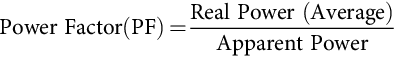
where the apparent power is defined as the product of rms values of instantaneous voltage vs(t) and instantaneous current is(t). It is well-known that if the load is linear, it draws purely sinusoidal current under sinusoidal voltage. In this case, the PF is only determined by the phase shift between vs(t) and is(t). Hence, Eq. (16.1) becomes

where Is,rms and Vs,rms are rms values of the current drawn by the load and the voltage applied to the load, respectively, and θ is the phase shift between instantaneous drawn current and instantaneous applied voltage. Hence, if the power system delivers a pure sine waveform voltage and the load is linear, the PF is simply equal to the cosine of the phase shift angle between the instantaneous current and instantaneous voltage. However, in power electronics system, due to the nonlinear behavior of active switching power devices, Eq. (16.2) is not valid anymore, and the phase-angle representation alone is not enough for the calculation of the PF which becomes more delicate. Fig. 16.1B shows a typical distorted current drawn from the pure sinusoidal power source. It is obvious that the calculation of the PF for distorted waveforms of the current or/and voltage is more complex when compared with the sinusoidal current and voltage waveforms. If both line voltage and line current are distorted, in this case Eqs. (16.3) and (16.4) give the Fourier expansion representations for the instantaneous drawn current and instantaneous power source voltage, respectively [1]:


Practically, the two DC (average value) of the instantaneous current and voltage that are expected to be seen from the power supply side are equal to zero due to the symmetry of the positive and negative parts of the voltage and current during one period; therefore, IDC=VDC=0. Applying the definition of PF given in Eq. (16.1) to the distorted current and voltage waveforms of Eqs. (16.3) and (16.4), PF may be expressed as:
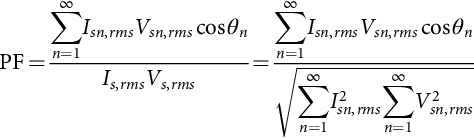
where Vsn,rms and Isn,rms are the rms values of the nth harmonic voltage and current, respectively, and θn is the phase shift between the instantaneous voltage and current corresponding to the nth harmonic ![]() .
.
Since most of power electronic systems draw their input voltage from a pure sine waveform power supply voltage vs(t), the above expression can be significantly simplified by assuming that the power supply voltage has a pure sine waveform and the distortion is only included in the instantaneous current is(t), that is,
Then, it can be shown that the PF can be expressed as

where
θ1: the phase-angle between the voltage vs(t) and the fundamental component of is(t),
Is1,rms: rms value of the fundamental component in line current,
Is,rms: total rms value of line current,
![]() : distortion factor,
: distortion factor,
![]() : displacement factor.
: displacement factor.
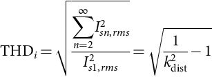
Another important parameter which measures the percentage of current distortion is known as the current total harmonic distortion (THDi), which is defined as follows:
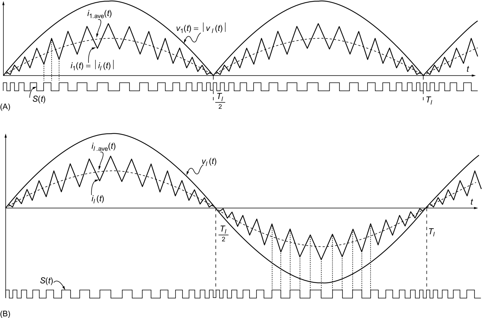
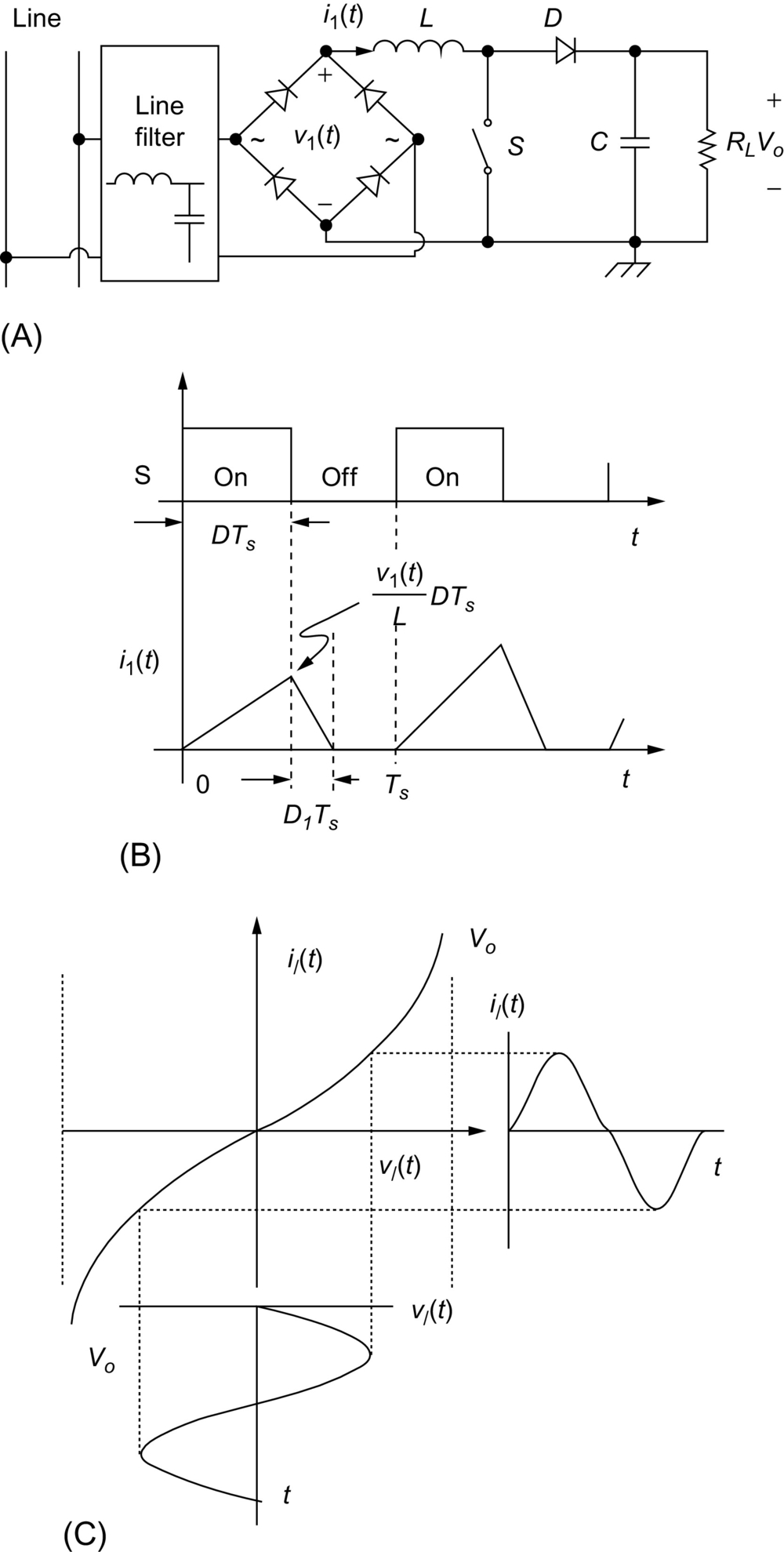
Conventionally, SMPSs use capacitive rectifiers in front of the ac line that results in the capacitor voltage vc and high rms pulsating line current il(t) as shown in Fig. 16.2, when vl(t) is the line voltage. The typical input current harmonic distortion THDi for this kind of rectification is usually in the range of 55%–65%, and the PF is about 0.65 [20,21]. It can be said also that the actual current wave shape and the resulting harmonics depend on the line impedance. This input current character creates several problems within the distribution network and consequently affecting the other electric apparatus in the vicinity of the rectifier. However, some solution has been proposed to overcome these drawbacks especially for high-power. The present chapter is focusing mainly on the study of the improvement of the current shape and PFC related to line current of single-phase rectifier followed by DC-DC converter that are mainly used for limited power level.

As we can see from Eqs. (16.8) and (16.9), PF and THD are related to distortion and displacement factors. Therefore, improvement in PF, that is, PFC, also implies harmonic reduction, especially the low order harmonics [1].
16.3 Power Factor Correction
16.3.1 Energy Balance in PFC Circuits
Fig. 16.3 shows a diagram of an AC-DC PFC unit. Let vi(t) and il(t) be the line voltage (the power source voltage) and line current (the drawn current from the power source), respectively. For an ideal PFC unit (![]() ), we assume
), we assume

where Vlm and Ilm are amplitudes of line voltage and line current, respectively, and ωl is the angular line frequency. The instantaneous input power is given by
where ![]() is constant value that is presenting the average of the instantaneous input power pin(t). It is important to clarify that only this part of power is contributing for the production of the effective energy that can be used by the load; therefore, it is often called the real power. On the other side, pin(t) possesses also an alternative component with frequency 2ωl as shown in Fig. 16.4 (i.e., 100 or 120 Hz, following the used power supply 50 or 60 Hz, respectively). Therefore, the operation principle of a PFC circuit is to process the input power in a certain way that it stores the excessive input energy when pin(t) is greater than
is constant value that is presenting the average of the instantaneous input power pin(t). It is important to clarify that only this part of power is contributing for the production of the effective energy that can be used by the load; therefore, it is often called the real power. On the other side, pin(t) possesses also an alternative component with frequency 2ωl as shown in Fig. 16.4 (i.e., 100 or 120 Hz, following the used power supply 50 or 60 Hz, respectively). Therefore, the operation principle of a PFC circuit is to process the input power in a certain way that it stores the excessive input energy when pin(t) is greater than ![]() and releases the stored energy when pin(t) is less than
and releases the stored energy when pin(t) is less than ![]() , where a compensation is achieved between the stored energy and the released energy in these two stages (Fig. 16.4). The average value between these two terms of energy is equal to zero. We can estimate the instantaneous excessive power as
, where a compensation is achieved between the stored energy and the released energy in these two stages (Fig. 16.4). The average value between these two terms of energy is equal to zero. We can estimate the instantaneous excessive power as

Hence, the instantaneous excessive input energy, wex(t), is given by

At ![]() and
and ![]() , the excessive input energy is null, and at
, the excessive input energy is null, and at ![]() , the excessive input energy reaches the peak value
, the excessive input energy reaches the peak value
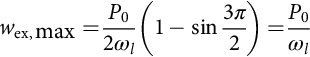
To achieve this concept of the dynamic behavior of the excessive input energy variation, the PFC circuit has to ensure this both functionality of storing the excessive energy and realizing the stored excessive energy by integrating the basic dynamic components (inductor and capacitor) in the PFC circuit. Indeed, in most of the PFC circuits that have been used in such applications, an input inductor is used to carry the line current. To obtain a unity PF, it is well obvious that the inductor current (or averaged inductor current in switch-mode PFC circuit) must be a pure sinusoidal and in phase with the line voltage. The energy stored in the inductor (1/2LiL2(t)) cannot completely match the change of the excessive energy as shown in Fig. 16.4. Therefore, to maintain the output power constant, another energy storage component (usually the output capacitor) is needed [1].
16.3.2 Passive Power Factor Corrector
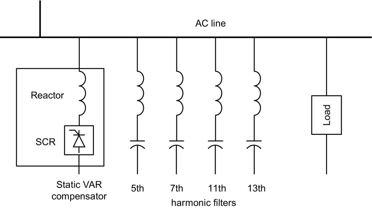
Because of their high reliability and high-power-handling capability, passive power factor correctors are normally used in high-power-line applications. Series-tuned LC harmonic filter is commonly used for heavy plant loads such as arc furnaces, metal rolling mills, and electric locomotives [1]. Fig. 16.5 shows a connection diagram of a selective low frequency harmonic filter together with line frequency switched reactor SVC. By tuning the filter branches to odd harmonic of low frequencies, the filter shunts the harmonic currents. Since each branch presents capacitive at line frequency, the filter also provides capacitive SVC for the system, whereas the integration of the thyristor-controlled reactor (TCR) in parallel with this selected group of low frequency filters keeps an optimized static var compensation for the system so that higher PF can be maintained.
The design of the tuned filter PF corrector is particularly difficult because of the uncertainty of the system impedance and the characteristics of the harmonic sources. Besides, this method involves too many expensive components and takes huge space in comparison with the active PFC method.
For the applications where the power level is less than 10 kW, the tuned filter PF corrector may not be a better choice. The most common off-line passive PF corrector is the inductive-input filter, shown in Fig. 16.6. This filter can operate either in the continuous conduction mode (CCM), in which the rectifier bridge is always conducting, or in the discontinuous conduction mode (DCM) where the rectifier is off during a portion of the line period [22,23]. A conduction parameter Kl is defined in the literature based on the values of the filter parameters, the inductance L, the assumed resistor R, and the line input frequency ωl as follows:

The assumed resistor represents the ratio between the average value of the voltage and the average value of the current at the output side of the filter.
For operation in CCM, the PF is defined as [22,23]:
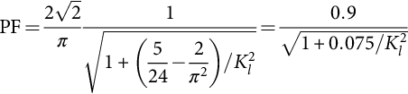
Depending on the filter inductance, this circuit can achieve a maximum PF of 90%, which is corresponding to the theoretical value of ![]() . On the other side, it was found in [22,23] that the critical value of Kl(Klcrit) that makes the minimum of the inductor current reach the zero value is
. On the other side, it was found in [22,23] that the critical value of Kl(Klcrit) that makes the minimum of the inductor current reach the zero value is ![]() ; this value makes the PF to fall to the value of 73.2%. In case where
; this value makes the PF to fall to the value of 73.2%. In case where ![]() , the current passes to the DCM [23].
, the current passes to the DCM [23].
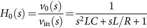
The PF corrector is simply a low-pass inductive filter as shown in Fig. 16.7, whose transfer function and input impedance are given by [1]


This kind of filter shown in Fig. 16.6 is characterized by the following main advantages:
(a) It has a simple structure.
(b) It is reliable.
(c) The cost is very low because only a filter is required.
(d) The high-frequency switching losses are absent, and it is not sensitive to noises and surges.
(e) The equipments used in this circuit do not generate high-frequency EMI.
The above equations show that the unavoidable phase displacement is incurred in the inductive filter corrector. Because the filter frequency of operation is low (line frequency), large value inductor and capacitor have to be used. As a result, the following main disadvantages are presented in the most passive PF correctors:
(a) Only less than 0.9 PF can be achieved.
(b) The output voltage cannot be regulated under uncontrolled rectifier.
(c) The efficiency is low.
(d) THD is high.
(e) It cannot provide satisfactory results for wide load range.
(f) They are heavy and bulky, because, for achieving a better power factor, the size of the filter increases.
(g) The output is unregulated.
(h) The dynamic response is poor due to the time lag associated with the passive elements.
(i) They are sensitive to circuit parameters.
(j) Although by filtering the harmonics that can be filtered out, the fundamental component may get phase-shifted, thus reducing the power factor.
(k) The shape of input current is dependent upon what kind of load is connected.
(l) Optimization of the design is difficult.
16.3.3 Basic Circuit Topologies of Active Power Factor Correctors
In recent years, using the switched-mode topologies, many circuits and control methods are developed up to date to comply with certain standard (such as IEEE Std 519 and IEC1000-3-2). To achieve this, high-frequency switching techniques have been used to shape the input current waveform successfully [1]. Basically, the active PF correctors that are used to accomplish the PFC function in single-phase power supply are based on the well-known basic converter topologies or their developed versions.
16.3.3.1 The Buck Corrector
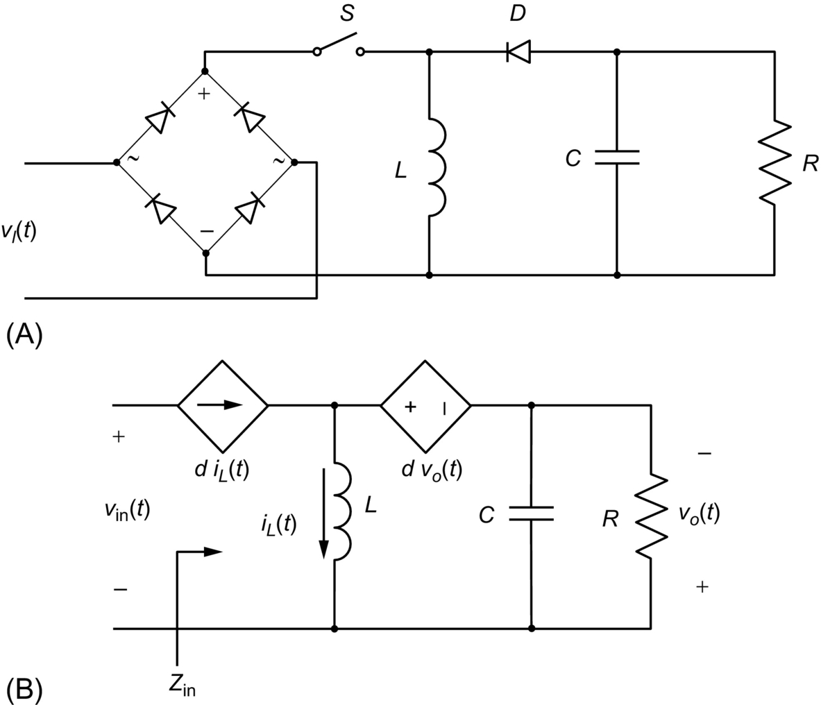
Fig. 16.8A shows the buck PF corrector. By using PWM switch modeling technique [24], the circuit topology can be modeled by the equivalent circuit shown in Fig. 16.8B. It should be pointed out that the circuit model is a large signal model; therefore, analysis of PF performance based on this model is valid. It can be shown that the transfer function and input impedance are given by [1]


where d is the duty ratio of the switching signal.
Notice that Eqs. (16.18) and (16.19) are different from Eqs. (16.16) and (16.17), in that they have introduced the control variable d. By properly controlling the switching duty ratio to modulate the input impedance and the transfer function, a pure resistive input impedance and constant output voltage can be approached [1]. Thereby, unity PF and output regulation can both be achieved. These control techniques will be discussed in the next section.
Comparing with the other type of high-frequency PFC circuits, the buck corrector offers inrush-current limiting, overload or short-circuit protection, and overvoltage protection for the converter due to the existence of the power switch in front of the line. Another advantage is that the output voltage is lower than the peak of the line voltage, which is usually the case normally desired. The drawbacks of using buck corrector may be summarized as follows [1]:
(a) When the output voltage is higher than the line voltage, the converter draws no current from the line, resulting in significant line current distortion near the zero-across of the line voltage.
(b) The input current is discontinuous, leading to high differential mode EMI.
(c) The current stress on the power switch is high.
(d) The power switch needs a floating drive.
16.3.3.2 The Boost Corrector
The boost corrector and its equivalent PWM switch modeling circuit are shown in Fig. 16.9A and B. Its transfer function and input impedance are given by [1]


where ![]() .
.
Unlike in the buck case, it is interesting to note that in the boost case, the equivalent inductance is controlled by the switching duty ratio. Consequently, both the magnitude and the phase of the impedance, and both the dc gain and the pools of the transfer function are modulated by the duty ratio, which implies a tight control of the input current and the output voltage. Other advantages of boost corrector include less EMI and lower switch current and grounded drive. The shortcomings with the boost corrector are summarized as [1]
(a) the output voltage must be higher than the peak of line voltage;
(b) inrush-current limiting, overload, and overvoltage protections are not available.
16.3.3.3 The Buck-Boost Corrector
The buck-boost corrector and its equivalent circuit are shown in Fig. 16.10A and B. The expressions for transfer function and input impedance are [1]


The buck-boost corrector combines some advantages of the buck corrector and the boost corrector. Like a buck corrector, it can provide circuit protections and step-down output voltage, and like a boost corrector its input current waveform and output voltage can be tightly controlled. However, the buck-boost corrector has the following disadvantages [1]:
(a) The input current is discontinued by the power switch, resulting in high differential mode EMI.
(b) The current stress on the power switch is high.
(c) The power switch needs a floating drive.
(d) The polarity of output voltage is reversed.
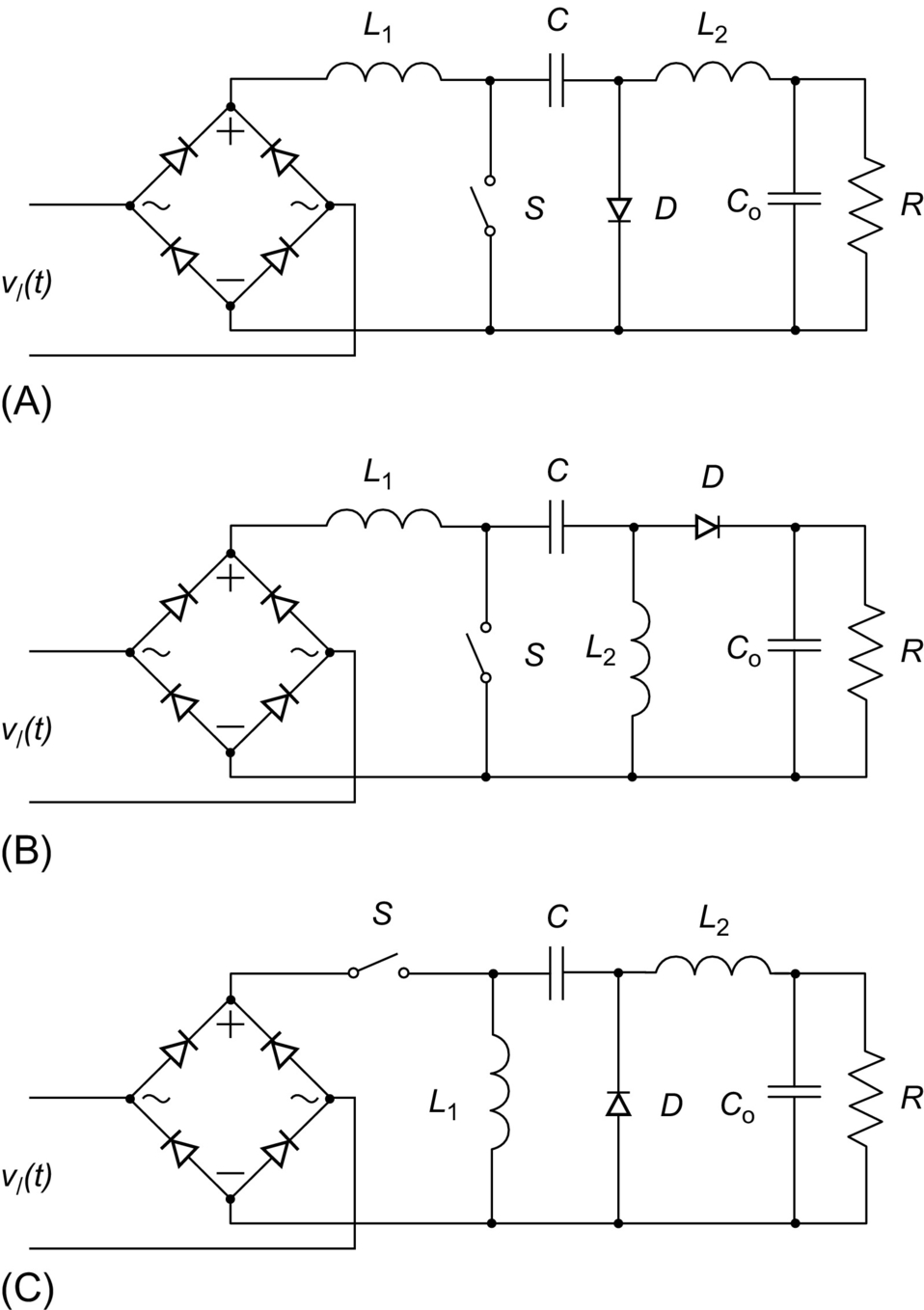
16.3.3.4 The Cuk, Sepic, and Zeta Correctors
Unlike the previous converters, the Cuk, Sepic, and Zeta converters are fourth-order switching-mode circuits. Their circuit topologies for PFC are shown in Fig. 16.11A–C, respectively. Because there are four energy storage components available to handle the energy balancing involved in PFC, second-harmonic output voltage ripples of these correctors are smaller when compared with the second-order buck, boost, and buck-boost topologies. These PF correctors are also able to provide overload protection. However, the increased count of components and current stress are undesired [1].
16.3.3.5 Flyback Corrector
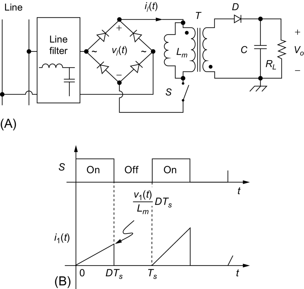
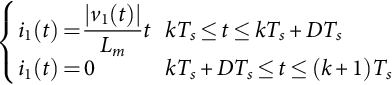
The flyback corrector allows to the input current to be shaped into a rectified sine wave, which is in phase with the input voltage, thus achieving a high PF and low harmonics content. Indeed, it is one of the most used active PFC converters, which has been widely used as an isolated front-stage PFC converter [25,26] and as a single-stage PFC [27–32]. Indeed, this topology presents many advantages such as isolation between input and output, low-cost, and simple structure. However, the large voltage stress on the primary switch and the large current stress through the output diode have limited its application to low-power level Fig. 16.12 [33–39].

The flyback PFC topology can operate under the three modes: continuous current mode (CCM), discontinuous current mode (DCM), and critical conduction mode (CRM). The operating mode is chosen upon the behavior of the freewheeling diode at the isolating transformer secondary side when the main switch “S” is turned off in one switch period.
The CCM operation of the flyback PFC converter requires two control loops. The first control loop is used to control the current to ensure the line current wave shape and a zero shift phase between the line voltage and line current, consequently a unity PF, can be obtained. The second control loop is used to control the output voltage to achieve its regulation. For DCM and CRM flyback PFC converters, only voltage control loop is required, which allows to obtained circuits that are simpler than that of CCM flyback PFC converter, this makes the DCM and CRM flyback PFC converters to be more widely used [35–42].
16.3.3.6 Forward, Forward-Flyback Correctors
The forward converter is presenting the simplest isolated buck-type converter, which has been widely applied for DC/DC conversions. The use of the basic topology and the practical topology shown in Fig. 16.13A and B of the forward converter for PFC applications include several disadvantages: (1) The typical single-ended forward converter requires a third additional auxiliary winding to ensure the transformer energy reset demagnetization [43], (2) it has the same drawbacks and limits of the basic topology of the buck PFC converter [43–45], and (3) as shown in Fig. 16.13A, when the output voltage V0 is greater than the input rectified voltage Vin, dead zones appear in the input current waveforms iin, that can degrade the PF and contribute to the increase of the harmonics content. These main disadvantages make the basic topology forward PFC difficult to be used in PFC applications. However, many works have presented improved topologies of this kind of converter to fulfill the requirement of decreased input current harmonics distortion and higher PF. One of such topologies that was proposed to overcome the main disadvantages of the basic topology of the forward converter is the forward-flyback PFC topology that combines the basic forward topology and the basic flyback topology, where only one common switch and one common transfer are used as shown in Fig. 16.13C [46–50]. In this topology, when the input voltage is not large enough to enable the forward operation, the flyback converter contributes to the power transfer. The main advantages of the proposed topology are the following [24,46–50]:

1. The dead zones existing in the convention forward PFC topology are eliminated.
2. The transformer is reset during the flyback converter operation.
3. The additional reset winding for the forward converter is no more needed.
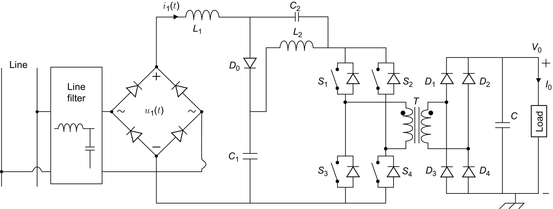
16.3.3.7 A Single-Stage Quasi Z-Source Corrector
The quasi-Z-Source (qZS) topology and their different improved topologies have been introduced recently in several DC-DC converter applications [51–53]. The single-stage qZS converter topology was proposed to ensure the PFC converter in single-phase application [54,55]. This topology, even it is different from the other topologies DC-DC converter topologies previously presented, but it has several features such as low-voltage stress on switches; lossless clamping, without using auxiliary switch; and duty-cycle-control scheme and improved efficiency. The circuit of this PFC converter is shown in Fig. 16.14. The single-phase power supply provides the line input to the load via the qZS, the full-bridge diode rectifier, and the transformer and the second full-bridge diode rectifier. The same control strategies that are used for the other DC-DC converter topologies are used for these topologies with more or less modifications, where the main aim is to shape the input line current into a sinusoidal wave and in phase with the input line voltage to obtain a unity PF.
16.3.4 System Configurations of PFC Power Supply
The most common configurations of AC-DC power supply with PFC are two-stage scheme and one-stage (or single-stage) scheme. In two-stage scheme as shown in Fig. 16.15A, a nonisolated PFC AC-DC converter is connected to the line to create an intermediate DC bus. This DC bus voltage is usually full of second-harmonic ripple and which is followed by a cascaded DC-DC converter to provide electric isolation and tight voltage regulation. The advantage of two-stage structure PFC circuits is that the two power stages can be controlled separately, and thus, it makes it possible to have both converters optimized. The drawbacks of this scheme are lower efficiency due to twice processing of the input power, two control systems which leads to complex control circuits, higher cost, bulky due to the used intermediary circuits between the two stages, and low reliability. Although the two-stage scheme approach is commonly adopted in several industrial applications, it received limited attention by the common research, since the input stage and the output stage can be studied independently. One-stage scheme possesses a simplified structure that combines the PFC circuit and the power conversion circuit in one-stage as shown in Fig. 16.15B. Therefore, this topology is potentially more efficient and is very attractive in low to medium power level applications, particularly in those cost-sensitive applications. The one-stage scheme, therefore, becomes the main stream of contemporary research due to the ever-increasing demands for inexpensive power supply applications, such as residential and office appliance [1].


For many single-stage PFC converters, one of the most important issues is the slow dynamic response under line and load changes. To remove the low frequency ripple caused by the line (120 or 100 Hz) from the output and keep a nearly constant operation duty ratio, a large volume output capacitor is normally used. Consequently, a low frequency pole (typically less than 20 Hz) must be introduced into the feedback loop. This results in very slow dynamic response of the system [1,56,57].
The behavior of energy transfer in single-phase PFC converter and the behavior of the required storage decoupling element can be understood through the representation of the converter instantaneous input power and the average output power waveforms in more details as shown in Fig. 16.17. It can be seen clearly that the converter has to transfer a peak power equals to twice the average output power, whereas this power has to be stored and then restored to the converter output side. Typically, an output capacitor (placed at the output side of the converter) is not the desired solution to store this energy for two reasons. Firstly, the output voltage possesses voltage fluctuation with double line frequency because tight output voltage regulation will require a small output capacitor. Secondly, the converter requires a holdup time. Therefore, the right solution is the use of a decoupling capacitor to ensure the main operation of storing and restoring the energy during the two stages. The location of the energy storage element becomes critical and general configuration of the topology will play an important role [58]. The waveform presented in Fig. 16.17 can be used to find the relation between P1 and P2 based on the calculation of the areas corresponding to each power:


It is found that 68.17% ![]() of the energy can be transferred directly to the output, and only 31.83%
of the energy can be transferred directly to the output, and only 31.83% ![]() of the energy has to be stored and then reprocessed to the output.
of the energy has to be stored and then reprocessed to the output.
It is obvious that the double frequency will be hidden from the output voltage ripple if P1 energy is directly transferred to the output due to the power storage excesses. Based on this analysis, improved and modified topologies of the basic converter topologies can be attained to achieve the direct energy transfer topology and the parallel energy transfer topology. Indeed, several works have been presented focusing mainly on the improvement of the PFC converter topology structure to ensure reduced number of components while delivering maximum energy directly to the output under enhanced efficiency [58–65].
To avoid twice power process in two-stage scheme, two converters can be connected in parallel to form so-called parallel PFC scheme (PPFC) as shown in Fig. 16.18 [66,67]. In parallel PFC circuit, power from the ac main to the load flows through two parallel paths, shown in Fig. 16.15C. The main path is a rectifier, in which power is not processed twice for PFC (about 68% of the average input power), whereas the other path processes the input power twice for PFC purpose. It is shown that to achieve both unity PF and tight output voltage regulation, only the difference between the input and output power within a half cycle (about 32% of the average input power) needs to be processed twice [1,66,67]. Therefore, high efficiency can be obtained by this method. In the PPFC topology, the common connection point of the two parallel paths appears at the output, where an isolation transformer is required for each stage (Fig. 16.18). Hence, this converter can be used effectively for the applications where the power level is high enough to justify the using of two isolations transformers that are too expensive and add more complexity to the converter topology [67].

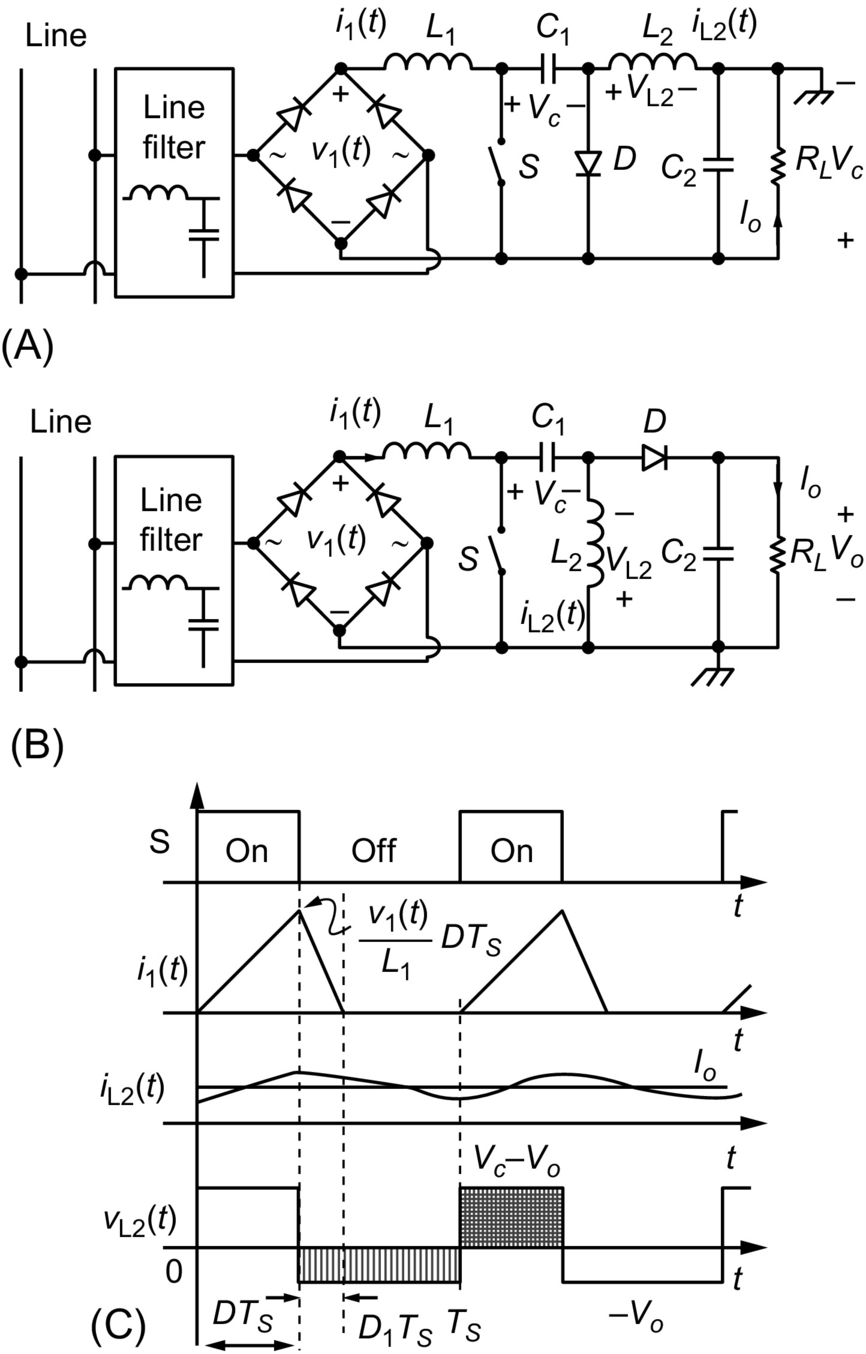
An improved topology has been used to avoid the main disadvantages of the presented PPFC of Fig. 16.18. It combines the auxiliary stage with the main stage, and, therefore, only one isolation transformer is required. This used PPFC topology power process transfer principle is shown in Fig. 16.19, where only one power stage is used to transfer the input power (Pin) and the extra 32% power (P2). Two application have been presented based on this PPFC topology, single-stage flyback PPFC converter and single-stage boost PPFC as shown in Fig. 16.20A and B; both topologies are using only one isolation transformer [67].

The continuous research in improving system PF up to date has resulted in countless circuit topologies and control strategies. Classified by their principles to realize PFC, they can be mainly categorized into three categories depending especially on the conduction current behavior of the input current of the converter that is related generally to the inductance of the equalizer PFC:
• Continuous conduction mode (CCM) that is based on the techniques of current shaping (current shaping technique (CST)) in Fig. 16.21
• Discontinuous conduction mode (DCM) that is based on current input control technique (CICT) in Fig. 16.22

• Critical conduction mode (CRM) that is similar to boundary conduction mode (BCM) or transition mode (TM) in Fig. 16.23

The recent research interest in DCM input technique is focused on developing PFC circuit topologies with a single power switch, result in single-stage single-switch converter (so-called S4-converter) [1]. The CCM shaping technique emphasizes on the used control strategies and on the improved topologies to achieve high input PF for medium and high-power levels. When this technique is applied for the control of a continuous flow of current, a fixed or a variable switching frequency can be used [68].
The CRM technique is on the boundary between CCM and DCM techniques. It was proved that it can ensure moderate switch losses, and in the same time, it can reduce the eventual diode reverse-recovery problems. The two main CRM PFC controller strategies of voltage mode and current mode can be used; however, the need to the voltage or the current sensors, depending on the used control strategy, adds more complexity to the used circuits [69].
The hot topics in this line of research are concentrated on degrading complexity of the control circuit and enhancing dynamic response of the system, resulting in some new control methods. Fig. 16.16 shows an overview of these techniques based on conduction mode and system configuration types [1]. It is obvious that the new developed and improved topologies based on the existing classical basic topologies can achieve the main objective of higher PF and lower THD than those of traditional topologies; this can be fulfilled by improving at the same time the control strategies for different modes of conduction.
16.4 CCM Shaping Technique
Like other power electronic apparatus, the core of a PFC unit is its converter, which can operate either in DCM, in CCM, or in CRM. As shall be discussed in the next section, the benefit from DCM technique is that low-cost power supply can be achieved because of its simplified control circuit. However, the peak input current of a DCM converter is at least twice as high as its corresponding average input current, which causes higher current stresses on switches than that in a CCM converter, resulting in intolerable conduction and switching losses and transformer copper losses in high-power applications. In practice, DCM technique is only suitable for low- to medium-level power application, whereas CCM is used in high-power cases. However, a converter operating in CCM does not have PFC ability inherently, that is, unless a certain control strategy is applied, the input current will not follow the waveform of line voltage. This is why most of the research activities in improving PF under CCM condition have been focused on developing new current shaping control strategies. Depending on the system variable being controlled (either current or voltage), PFC control techniques may be classified as current control and voltage control. Current control is the most common control strategy since the primary objective of PFC is to force the input current to trace the shape of line voltage [1].
To achieve both PFC and output voltage regulation by using a converter operating in CCM, multiloop controls are generally used. Fig. 16.24 shows the block diagram of AC-DC PFC converter with CCM shaping technique, where Hl is a line voltage compensator, Hx is a controlled variable compensator, and x(t) is the control variable that can be either current or voltage [1].

Normally, in order to obtain a sinusoidal line current and a constant dc output voltage, line voltage vl(t), output voltage Vo, and a controlled variable x(t) need to be sensed. Depending on whether the controlled variable x(t) is a current (usually the line current or the switch current) or a voltage (related to the line voltage or rectified line voltage), the control technique is called “current mode control” or “voltage mode control,” respectively. In Fig. 16.24, two control loops have been applied: the feedforward loop and the feedback loops. The feedforward loop is also called “inner loop,” which keeps the line current to follow the line voltage in shape and phase, while the feedback loop (also called “outer loop”) keeps the output voltage to be tightly controlled. These two loops share the same control command generated by the product of output voltage error signal and the line voltage (or rectified line voltage) signal [1].
16.4.1 Current Mode Control
Over many years, different current mode control techniques were developed. In this section, we will review several known methods.
16.4.1.1 Average Current Control
In average current control (ACM) strategy, the average line current of the converter is controlled to be shaped to a sine waveform which in phase with the line voltage. It is more desired than the other control strategies because the line current in a SMPS can be approximated by the average current (per switching cycle) through an input EMI filter. This control strategy is widely used in several industries due to the improved noise immunity, the lower input ripple, and the stable operation [56,70–73].
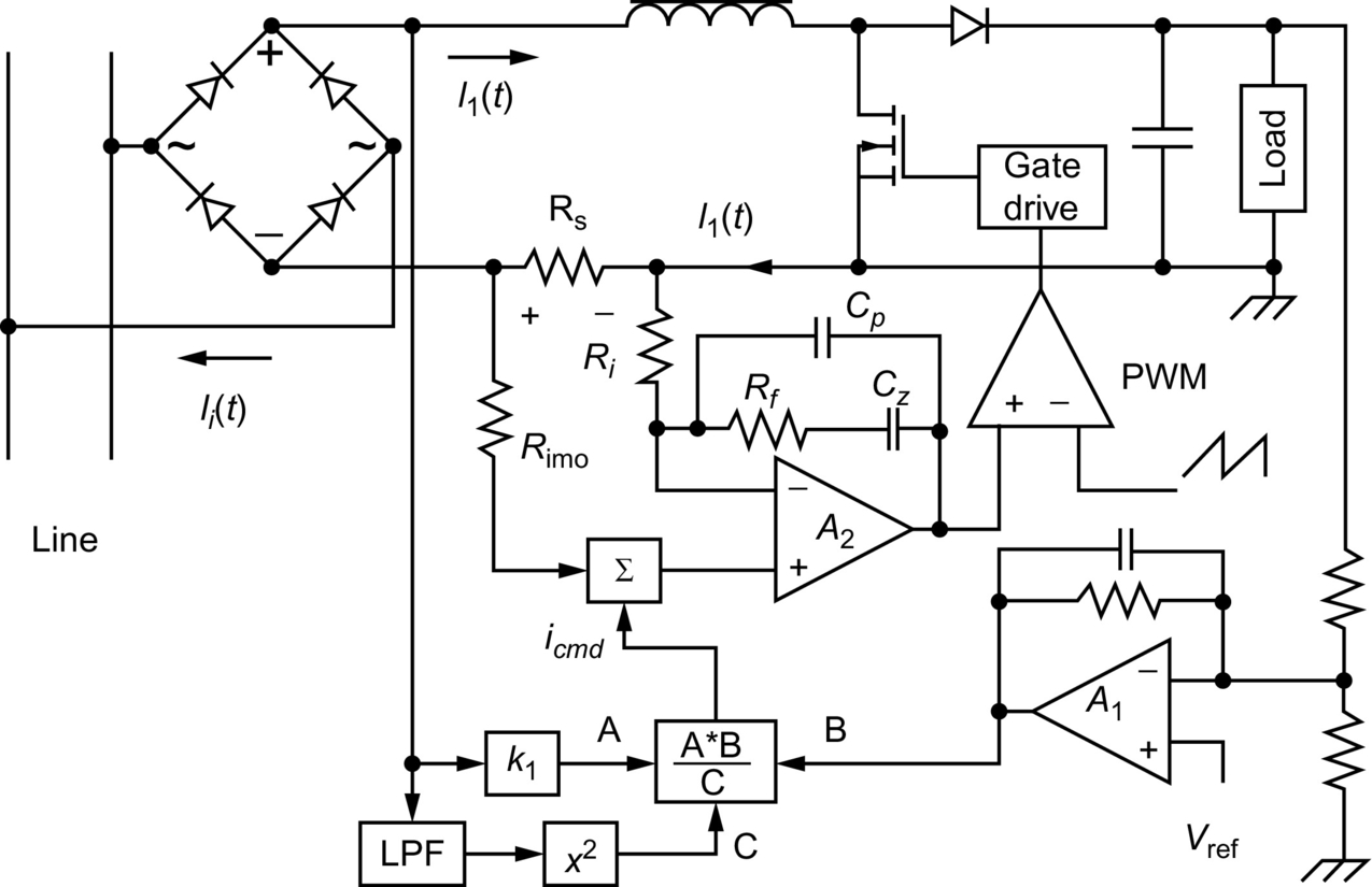
Fig. 16.22 shows a boost PFC circuit using ACM strategy. In the feedforward loop, a low value resistor Rs is used to sense the line current. Through the op-amp network formed by Ri,Rimo,Rf,Cp,Cz,andA2, average line current is detected and compared with the command current signal, icmd, which is generated by the product of line voltage signal and the output voltage error signal.
There is a common issue in CCM shaping technique, that is, when the line voltage increases, the line voltage sensor provides an increased sinusoidal reference for the feedforward loop. Since the response of feedback loop is much slow than the feedforward loop, both the line voltage and the line current increase, that is, the line current is heading to wrong changing direction (with the line voltage increasing, the line current should decrease). This results in excessive input power, causing overshoot in the output voltage. The square block, x2, in the line voltage-sensing loop shown in Fig. 16.25 provides a typical solution for this problem. It squares the output of the low-pass filter (LPF), which is in proportion to the amplitude of the line voltage and provides the divider ![]() with a squared line voltage signal for its denominator. As a result, the amplitude of the sinusoidal reference icmd is negatively proportional to the line voltage, that is, when the line voltage changes, the control circuit leads the line current to change in the opposite direction, which is the desired situation. The detailed analysis and design issues can be found in [1,70–72].
with a squared line voltage signal for its denominator. As a result, the amplitude of the sinusoidal reference icmd is negatively proportional to the line voltage, that is, when the line voltage changes, the control circuit leads the line current to change in the opposite direction, which is the desired situation. The detailed analysis and design issues can be found in [1,70–72].
As it can be seen, the ACM is a very complicated control strategy. It requires sensing the inductor current, the input voltage, and the output voltage. An amplifier for calculating the average current and a multiplier are needed. Actually, due to the advances made in IC technology, these circuits are integrated in a single chip, where many control ICs are available from different manufacturers.
16.4.1.2 I2 Average Current Mode Control
This control technique is proposed to improve the transient response and the light load efficiency of the existing average current mode control [74]. The main principle of this control technique is applied to buck converter as shown in Fig. 16.26. It is based on the use of three loops, two current inner loops and one voltage outer loop. The first current loop presents a slow integral feedback that integrates the error between the output voltage of the voltage loop Vc and the current through Ls. The second current loop presents a fast direct feedback of the current through Ls without LPF that is compared with the integrator output of the first current loop to generate the PWM signal. The third loop is dedicated to ensure the output voltage regulation. As the current through Ls is measured once and it is used twice in the two control loops, the proposed control technique is named as I2 control. In general, this concept is applicable to constant frequency modulations and variable frequency modulations [74,75].

16.4.1.3 Variable Frequency Peak Current Control
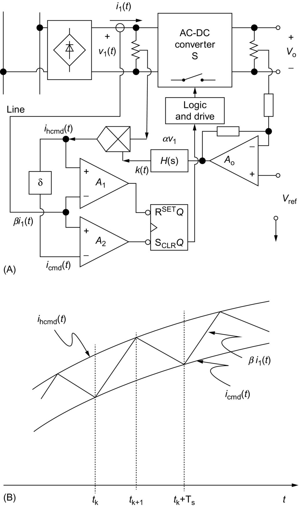
Although the ACM is a more desired strategy, the peak current control has been widely accepted because it improves the converter efficiency and has a simpler control circuit [57,76–80]. In variable frequency peak control strategy, shown in Fig. 16.27, the output error signal k(t) is fed back through its outer loop. This signal is multiplied by the line voltage signal αv1(t) to form a line current command signal icmd(t) (![]() ). The command signal icmd(t) is the desired line current shape since it follows the shape of the line voltage. The actual line current is sensed by a transducer, resulting in signal βi1(t) that must be reshaped to follow icmd(t) by feeding it back through the inner loop. After comparing the line current signal βi1(t) with the command signal icmd(t), the following control strategies can be realized, depending on its logic circuit [1]:
). The command signal icmd(t) is the desired line current shape since it follows the shape of the line voltage. The actual line current is sensed by a transducer, resulting in signal βi1(t) that must be reshaped to follow icmd(t) by feeding it back through the inner loop. After comparing the line current signal βi1(t) with the command signal icmd(t), the following control strategies can be realized, depending on its logic circuit [1]:

Constant on-time control: Its input current waveform is given in Fig. 16.28A. Letting the fixed on time to be Ts, the control rules are the following:

• At ![]() , S is turned off.
, S is turned off.
Constant off-time control: The input current waveform is shown in Fig. 16.28B. Assuming the offtime is Toff, the control rules are the following:
• At ![]() , S is turned on.
, S is turned on.
16.4.1.4 Constant Frequency Peak Current Control
Generally speaking, to make it easier to design the EMI filter and to reduce harmonics, constant switching frequency AC-DC PFC converter is preferred. Based on the block diagram shown in Fig. 16.29, with Ts is the switching period, the following control rules can be considered to realize a constant frequency peak current control (shown in Fig. 16.30B) [1]:


• At ![]() when
when ![]() , S is turned off.
, S is turned off.
The logic circuit for the above control rules can be realized by using an R-S flip-flop with a constant frequency setting clock pulse (CP), as shown in Fig. 16.29. Unfortunately, this logic circuit will result in instability when the duty ratio exceeds 50%. This problem can be solved by subtracting a stabilizing ramp signal from the original command signal. Fig. 16.30A shows a complete block diagram for typical constant frequency peak current control strategy. The line current waveform is shown in Fig. 16.30B [1].
It should be noticed that in both variable frequency and constant frequency peak current control strategies, either the input current or the switch current could be controlled. Thus, it makes possible to apply these control methods to buck-type converters. There are several advantages of using peak current control [1]:
• The peak current can be sensed by current transformer, resulting in reduced transducer loss.
• The current-error compensator for average control method has been eliminated.
• Low gain in the feedforward loop enhances the system stability.
• The instantaneous pulse-by-pulse current limit leads to increased reliability and response speed.
However, the three signals, line voltage, peak current, and output voltage signals, are still necessary to be sensed and multiplier is still needed in each of the peak current control method. Comparing with the ACM method, the input current ripple of these peak current control methods may be high when the line voltage is near the peak value. As a result, considerable line current distortion exists under high-line voltage and light low operation conditions [1].
16.4.1.5 Hysteresis Control
Unlike the constant on-time (COT) and the constant off-time control, in which only one current command is used to limit either the minimum input current or the maximum input current, the hysteresis control has two current commands, ihcmd(t) and ilcmd(t) (![]() ); δis the hysteresis band width which is supposed to be constant to limit both the minimum and the maximum of input current [81–84]. To achieve smaller ripple in the input current, we desire a narrow hysteresis band. However, with a reduced hysteresis band width a higher switching frequency is required. Therefore, the hysteresis bandwidth should be optimized based on circuit components such as switching devices and magnetic components. Moreover, the switching frequency varies with the change of line voltage, resulting in difficulty in the design of the EMI filter. The circuit diagram and input current waveform are given in Fig. 16.31A and B, respectively. When
); δis the hysteresis band width which is supposed to be constant to limit both the minimum and the maximum of input current [81–84]. To achieve smaller ripple in the input current, we desire a narrow hysteresis band. However, with a reduced hysteresis band width a higher switching frequency is required. Therefore, the hysteresis bandwidth should be optimized based on circuit components such as switching devices and magnetic components. Moreover, the switching frequency varies with the change of line voltage, resulting in difficulty in the design of the EMI filter. The circuit diagram and input current waveform are given in Fig. 16.31A and B, respectively. When ![]() , a negative pulse is generated by comparator A1 to reset the R-S flip-flop. When
, a negative pulse is generated by comparator A1 to reset the R-S flip-flop. When ![]() , a negative pulse is generated by comparator A2 to set the R-S flip-flop. The control rules are the following:
, a negative pulse is generated by comparator A2 to set the R-S flip-flop. The control rules are the following:
• At ![]() when
when ![]() , S is turned off.
, S is turned off.
Like the above mentioned peak current control methods, the hysteresis control method has simpler implementation, enhanced system stability, and increased reliability and response speed. In addition, it has better control accuracy than that the peak current control methods have. However, this improvement is achieved on the penalty of wide range of variation in the switching frequency. It is also possible to improve the hysteresis control in a constant frequency operation [85,86], but usually, this will increase the complexity of the control circuit [1].
16.4.1.6 Charge Control
In order to make the average control method to be applicable for buck-derived topologies where the switch current instead of the inductor current needs to be controlled, an alternative method to realize ACM, namely, charge control was proposed in [87–89]. Since the total charge of the switch current per switching cycle is proportional to the average value of the switch current, the average current can be detected by a capacitor-switch network. Fig. 16.32 shows a block diagram for charge control. The switch current is sensed by current transformer T1 and charges the capacitor CT to form average line current signal. As the switch current increases, the charge on capacitor CT also increases. When the voltage reaches the control command vc, the power switch turns off. At the same time, the switch Sd turns on to reset the capacitor. The next switching cycle begins with the power switch turning on and the switch Sd turning off by a CP [1].

The advantages of charge control are the following:
• Ability to control average switch current
• Better switching noise immunity than peak current control
• Good dynamic performance
• Elimination of turn-off failure in some converters (e.g., multiresonant converter) when the switch current reaches its maximum value
The disadvantages are the following:
• Synthesis of the reference vc still requires sensing both input and output voltage and use of a multiplier.
• Subharmonic oscillation may exist.
16.4.1.7 Nonlinear-Carrier Control
To further simplify the control circuitry, nonlinear-carrier (NLC) control methods were introduced [90,91]. In CCM operation, since the input voltage is related to the output voltage through the conversion ratio, the input voltage information can be recovered by the sensed output voltage signal. Thus, the sensing of input voltage can be avoided, and therefore, the multiplier is not needed, resulting in significant simplification in the control circuitry. However, complicated NLC waveform generator and its designs are involved. Fig. 16.33 shows the block diagram of the NLC charge control first introduced in [90,1].

16.4.2 Voltage Mode Control
Generally, current mode control is preferred in current source driven converters, as the boost converter. To develop controllers for voltage source driven converter, like the buck converter and to improve dynamic response, voltage mode control (VMC) strategy was proposed [92,93]. Fig. 16.34 shows the input circuit of an AC-DC converter and its phasor diagram representation, where ϕ is the phase shift between the line current and the capacitor voltage. An LC network could be added to the input either before a switch-mode rectifier (SMR) or after a passive rectifier to perform such kind of control. In boost type converter, the inductor Li is the input inductor. It can be seen from the phasor diagram that to keep the line current in phase with the line voltage, we can control either the capacitor voltage or the inductor voltage. If the capacitor voltage is chosen as controlled variable, the control strategy is known as delta modulation control [1].
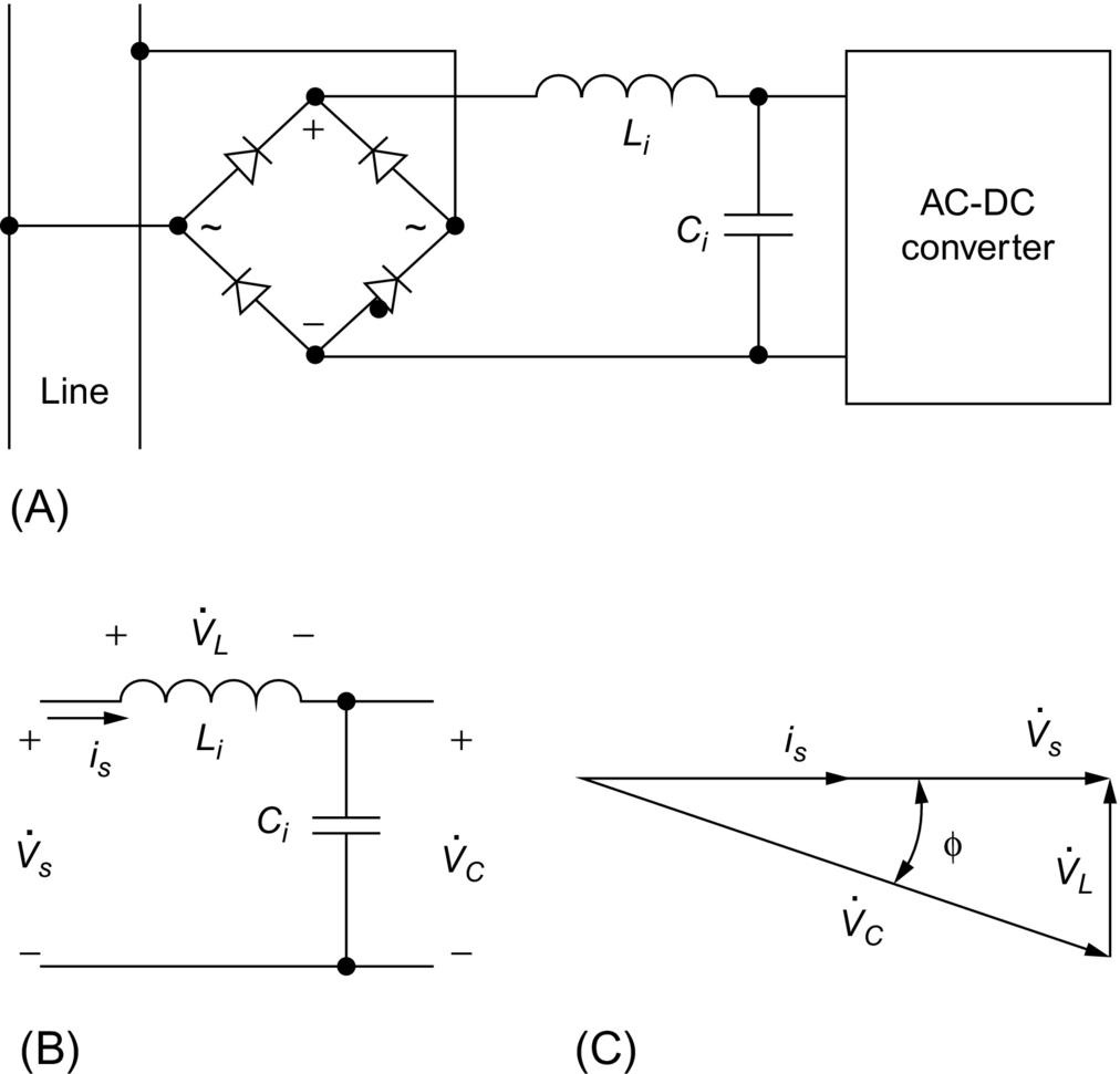
16.4.2.1 Capacitor Voltage Control
Fig. 16.35 gives a SMR with PFC using capacitor voltage control [92]. The capacitor voltage vc1(t) is forced to track a sinusoidal command signal vc1⁎(t) to indirectly adjust the line current il(t) to be in phase with the line voltage vl(t). The command signal is the product of the line voltage signal with a phase shift of ϕ and the feedback error signal. The phase shift ϕ that has to be measured accurately is a function of the magnitudes of line voltage and line current; therefore, achieving the delta modulation control is not really simple. In addition, since ϕ is usually very small, a small change in capacitor voltage that may occur due to small load change or to small output voltage reference change Vref will cause a large change in the inductor voltage and hence in the line current. Thus, it makes the circuit very sensitive to parameter variations and perturbations [1].

16.4.2.2 Inductor Voltage Control
To overcome the above shortcomings, inductor voltage control (IVC) strategies were reported in [93]. Fig. 16.36 shows an SMR with PFC using IVC. As the phase difference between the line voltage and the inductor voltage is fixed at 90 degrees ideally, the control circuit is simpler in implementation than that of capacitor voltage control. As the inductor voltage is sensitive to the phase shift ϕ, but not sensitive to the change in magnitude of reference, the IVC method is more effective in keeping the line current in phase with the line voltage. However, in the implementations of both the two kinds of voltage control methods hysteresis technique is normally used. Therefore, unlike the previous current mode control, variable frequency problem is encountered in these control methods [1].

Generally speaking, by using CCM shaping technique, the input current can trace the wave shape of the line voltage well. Hence, the PF can be improved efficiently. However, this technique involves in the designing of complicated control circuits. Multiloop control strategy is needed to perform ICS and output regulation. In most CCM shaping techniques, current sensor and multiplier are required, which result in higher cost in practical applications. In some cases, variable frequency control is inevitable, resulting in additional difficulties in its closed-loop design. Table 16.1 gives a comparison among these control methods [1].
Table 16.1
Comparison of CCM shaping techniques
| Average current | I2 average current | VF peak current | CF peak current | Hysteresis | Charge | Nonlinear-carrier | Capacitor voltage | Inductor voltage | |
| Input ripple | Low | Low | High | High | Low | Low | Low | Low | Low |
| Switching frequency | Constant | Constant and variable | Variable | Constant | Variable | Constant | Constant | Variable | Variable |
| Dynamic response | Slow | Improved transient response | Slow | Slow | Fast | Fast | Fast | Fast | Fast |
| Control signal sensed for inner loop | Input current and input voltage | Two input current and input voltage | Input (or switch) current and input voltage | Input (or switch) current and input voltage | Input current and input voltage | Input (or switch) current and input voltage | Input (or switch) current | Input voltage and capacitor voltage | Input voltage and inductor voltage |
| Inner loop E/A | Yes | Yes | No | No | Yes | No | No | No | No |
| Multiplier | Yes | No | Yes | Yes | Yes | Yes | No | Yes | Yes |

16.5 DCM Input Technique
The DCM can be considered as a special case of the CCM. It presents more than one structural change during one switching period. To get rid of the complicated control circuit invoked by CCM shaping technique and reduce the cost of the electronic interface, DCM input technique can be adopted in low-power to medium power level application.
In DCM, the inductor current of the core converter is no longer a valid state variable since its state in a given switching cycle is independent of the value in the previous switching cycle [94]. The peak of the inductor current is sampling the line voltage automatically, resulting in sinusoidal-like average input current (line current). This is why DCM input circuit is also called “voltage follower” or “automatic controller” [1]. The benefit of using DCM input circuit for PFC is that no feedforward control loop is required, because with this approach, the internal current loop is completely eliminated, so that the switch is operated at COT and frequency. This is also the main advantage over a CCM PFC circuit, in which multiloop control strategy is essential. However, the input inductor operating in DCM cannot hold the excessive input energy because it must release all its stored energy before the end of each switching cycle. As a result, a bulky capacitor is used to balance the instantaneous power between the input and output. In addition, in DCM, the input current is normally a train of triangle pulses with nearly constant duty ratio. In this case, an input filter is necessary for smoothing the pulsating input current [1]. With the converter working in DCM, the DCM PWM control technique allows unity PF when used with converter topologies like flyback, Cuk, and Sepic. Instead, with the boost PFC, this technique causes some harmonic distortion in the line current [95].
16.5.1 PFC Capabilities of the Basic Converter Topologies in DCM
The DCM input circuit can be one of the basic DC-DC converter topologies. However, when they are applied to the rectified line voltage, they may draw different shapes of average line current. In order to examine the PFC capabilities of the basic converters, we first investigate their input characteristics. Because the input currents of these converters are discrete when they are operating in DCM, only averaged input currents are considered. Since switching frequency is much higher than the line frequency, let's assume the line voltage is constant in a switching cycle. In steady state operation, the output voltage is nearly constant, and the variation in duty ratio is slight. Therefore, constant duty ratio is considered in deriving the input characteristics [1]. To simplify the analysis of different topologies of converter working in DCM for achieving the main objective of current shaping, the following assumptions were made:
2. The duty ratio of the converter is kept constant throughout the entire line cycle.
3. The switching frequency is much higher than the line frequency.
4. The leakage inductances of transformers are negligible.
5. Despite of slight changes in DC bus voltage, it is considered to be constant during each line cycle.
16.5.1.1 Buck Converter
The basic buck converter topology and its input current waveform when operating in DCM are shown in Fig. 16.37A and B, respectively. The instantaneous output current of the rectifier is presented as follows:
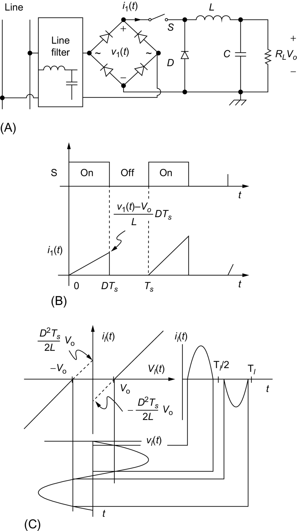

It can be shown that the average output current of the rectifier in one switching cycle is given by
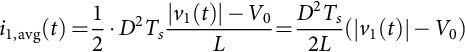
The average line current or the average input current of the rectifier during one switching cycle is given as follows:
Where it is supposed that the input voltage waveform is sinusoidal and the drop voltage along the rectifier is neglected. Based on Eq. (16.27), Fig. 16.37C shows that the input voltage-input current I-V characteristic consists of two straight lines in quadrants I and III. These straight lines that are presenting the average instantaneous input current versus the input voltage do not go through the origin. It is obvious that the instantaneous average value of the input current is equal to zero within the interval ![]() . When
. When ![]() , positive input current would occurs when
, positive input current would occurs when ![]() and negative input current occurs. As a result, due to the zero regions of the input current as shown in Fig. 16.37C. The input current is distorted simply because the buck converter can work only under the condition when the input voltage is larger than the output voltage. Therefore, the basic buck converter cannot fulfill the requirement of a good candidate that can be used to achieve the DCM input PFC.
and negative input current occurs. As a result, due to the zero regions of the input current as shown in Fig. 16.37C. The input current is distorted simply because the buck converter can work only under the condition when the input voltage is larger than the output voltage. Therefore, the basic buck converter cannot fulfill the requirement of a good candidate that can be used to achieve the DCM input PFC.
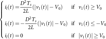
16.5.1.2 Boost Converter
The basic boost converter and its input current waveform are shown in Fig. 16.38A and B, respectively. This current can be presented by the following expression:

The average instantaneous input current of the boost converter in one switching cycle is given as follows:

where DTs is the interval of time during which the inductor current increases from zero to the current peak and D1Ts is the time during which the inductor current decreases from the current peak to zero.
The average line current or the average input current of the rectifier during one switching cycle is given as follows:
By plotting Eq. (16.32), we obtain the input I-V characteristic curve as given in Fig. 16.35C. As we can see that as long as the output voltage is larger than the peak value of the line voltage in certain range, the relationship between v1(t) and i1,avg(t) is nearly linear. When the boost converter is connected to the line, it will draw almost sinusoidal average input current from the line, shown as in Fig. 16.38C [1].
Because of the above reasons, boost converter is comparably superior to most of the other converters when applied to do PFC. However, it should be noted that boost converter can operate properly only when the output voltage is higher than its input voltage. When low-voltage output is needed, a step-down DC-DC converter must be cascaded [1].
16.5.1.3 Buck-Boost Converter
Fig. 16.39A shows a basic buck-boost converter topology; its input current waveform is shown in Fig. 16.39B. This current can be presented by the following expression:


The averaged input current of this converter can be found according to Eq. (16.33) as follows:

The average line current or the average input current of the rectifier during one switching cycle is given as follows:
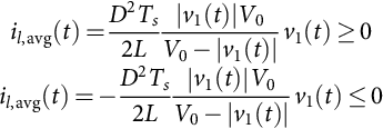
Eq. (16.35) gives a perfect linear relationship between il,avg(t) and v1(t), which proves that the buck-boost topology has an excellent automatic PFC property. It is obvious that the input current of this kind of converter is independent of the discharging behavior of the inductor. Its input I-V characteristics and input voltage and current waveforms are shown in Fig. 16.39C. Furthermore, the main objective of the buck-boost converter is to ensure an output voltage that can be either higher or lower than the input voltage; in the same time and due to the continuous linear relationship between il,avg(t) and v1(t) based on the DCM technique, this topology demonstrates strong availability to achieve a sine waveform of the input current and in phase with the input voltage that means a good PFC function.
Theoretically, buck-boost converter is a perfect candidate. Unfortunately, this topology has two limitations: (1) The polarity of its output voltage is reversed, that is, the input voltage and the output voltage cannot have the common ground, and (2) it needs floating drive for the power switch. The first limitation circumscribes this circuit into a very narrow scope of applications. As a result, it is not widely used [1].
16.5.1.4 Flyback Converter
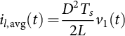
Flyback converter is an isolated converter whose topology is presented in Fig. 16.40A; its input current waveform is shown in Fig. 16.40B, and it is presented by the following equation:
It can be seen clearly that this current is similar to the buck-boost converter input current, where Lm is the magnetizing inductance of the output transformer. The averaged input current of this converter can be found according to Eq. (16.36) as follows:
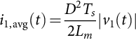
The average line current or the average input current of the rectifier during one switching cycle is given as follows:

Therefore, the flyback converter topology has the same input I-V characteristic as the buck-boost converter topology, and hence, it has the same input voltage and input current waveforms as shown in Fig. 16.40C.
Comparing with buck-boost converter, flyback converter has all the advantages of the buck-boost converter. What's more, input-output isolation can be provided by flyback converter. These advantages make flyback converter well suitable for PFC with DCM input technique. Comparing with boost converter, the flyback converter has better PFC, and the output voltage can be either higher or lower than the input voltage. However, due to the use of power transformer, the flyback converter has some drawbacks such as high di/dt noise, lower efficiency, and lower density (larger size and heavier weight) [1].
16.5.1.5 Forward Converter
The forward converter topology is shown in Fig. 16.41. In order to avoid transformer saturation, it is well-known that forward converter needs the third winding to demagnetize (reset) the transformer.

The forward converter topology, when compared with the flyback topology, has the advantages of lower peak output current and less leakage energy-related problems; it is generally more energy efficient, and it is used for applications requiring little higher power output (in the range of 100–200 W). However, the circuit topology, especially the output filtering circuit, is not as simple as in the flyback converter, and when its basic topology is connected to the rectified line voltage, the path of the demagnetizing current through the third winding is blocked by the rectifier bridge diodes during the turn-off period of the main switch S. Moreover, energy transfer to output ceases during the interval when the rectified input voltage |v1(t)| is lower than the reflected output voltage on the primary (i.e., ![]() ), resulting in distorted input current. Therefore, this basic topology cannot be used to achieve the PFC purpose unless a certain circuit modification is applied such as forward converter with a resistor-capacitor-diode (RCD) clamp circuit, the forward converter with an active clamp (FAC).
), resulting in distorted input current. Therefore, this basic topology cannot be used to achieve the PFC purpose unless a certain circuit modification is applied such as forward converter with a resistor-capacitor-diode (RCD) clamp circuit, the forward converter with an active clamp (FAC).
16.5.1.6 Cuk Converter and Sepic Converter
It can be shown that Cuk converter and Sepic converter given in Fig. 16.42A and B, respectively, have the same input I-V characteristic. Each of these converter topologies has two inductors, with one located at its input and the other at its output. Let's consider the case when the input inductor operates in DCM, while the output inductor operates in CCM. In this case, the capacitor C1 can be designed with large value to balance the instantaneous input/output power, resulting in high PF in the input and low second-harmonic ripple in the output voltage. To investigate the input characteristic of these converters, let's take the Cuk converter as an example. One should note that the results from the Cuk converter are also suitable for Sepic converter [1].
For the Cuk converter shown in Fig. 16.42A, the waveforms for input inductor current (the same as the input current), output inductor current, and the voltage across the output inductor are depicted in Fig. 16.42C [1]. Assume that the capacitor C1 is large enough to be considered as a voltage source Vc, in steady state, employing volt-second equilibrium principle on L2, we obtain
The input inductor current (the same as the input converter current) can be presented by the following expression:

The input inductor current reset time ratio D1 is given by

Therefore the averaged input current can be found as
It can be seen that Eq. (16.42) is very similar to Eq. (16.32) except that the denominator in the former equation is (![]() ) instead of (
) instead of (![]() ). This will lead to some improvement in that I-V characteristic in Cuk converter. Referring to the I-V characteristic shown in Fig. 16.38C, Cuk converter has a curve more close to a straight line. Such improvement, however, is achieved at the expense of using more circuit components. It can be proved that the same results can be obtained by the Sepic converter [1].
). This will lead to some improvement in that I-V characteristic in Cuk converter. Referring to the I-V characteristic shown in Fig. 16.38C, Cuk converter has a curve more close to a straight line. Such improvement, however, is achieved at the expense of using more circuit components. It can be proved that the same results can be obtained by the Sepic converter [1].
16.5.1.7 Zeta Converter
Fig. 16.43A gives a Zeta converter connected to the line. In DCM operation, the key waveforms are illustrated in Fig. 16.43B, where we presume the capacitor being equivalent to a voltage source Vc. As we can see that the converter input current waveform is exactly the same as that drawn by a buck-boost converter [1]. Thus, the instantaneous input current for the Zeta converter is identical to that for the buck-boost converter. It is expressed as follows:

The averaged input current of this converter can be found according to Eq. (16.43) as follows:
The average line current or the average input current of the rectifier during one switching cycle is given as follows:
which is the same as the one given by Eq. (16.33). As a result, the Zeta converter has as good automatic PFC capability as the buck-boost converter. The improvement achieved here is the noninverted output voltage. However, like the buck converter, floating drive is required for the power switch [1].
Based on the above discussion, we may conclude that all the eight basic converters except forward converter have good inherent PFC capability and are available for DCM PFC usage. Among them, boost converter and flyback converter are especially suitable for single-stage PFC scheme because they have minimum component count and grounded switch drive, and their power switches are easy to be shared with the output DC-DC converter. Hence, these two converters are most preferable by the designers for PFC purpose. The other converters could also be used to perform certain function such as circuit protection and small output voltage ripple. The characteristics of the eight basic converter topologies are summarized in Table 16.2 [1].
Table 16.2
Comparison of basic converter topologies operating for DCM input technique
| Buck | Boost | Buck-boost | Flyback | Forwarda | Cuk and Sepic | Zeta | |
| Line current waveform |  |
 |
 |
 |
– |  |
 |
| Switch drive | Floating | Grounded | Floating | Grounded | Grounded | Grounded | Floating |
| Peak input current | High | Lower | High | High | — | Lower | High |
| Inrush and overload protection | Yes | No | Yes | Yes | — | Yes | Yes |
| Output voltage | Inverted | — | |||||
| Power level | Low to medium | Low to medium | Low to medium | Low | — | Low to medium | Low to medium |

a The standard forward converter is not recommended as a PF corrector since the rectifier at the input will block the demagnetizing current through the tertiary winding.
16.5.1.8 Flyboost Converter
Unlike the aforementioned converter used for PFC applications, the flyboost converter was proposed in [96,97] to benefit simultaneously from the advantages of both flyback power transfer and boost power transfer. This proposed topology gains the features of the flyback and boost converter from point of view of power transfer process to achieve a unify PF and a very reduced input current harmonics. Indeed, it can be said that the difference of this topology from the basic topologies such as boost, SEPIC, buck-boost, Cuk, and buck is not so important; however, the operation principle is very different. It is obvious that there are only two operation modes for flyboost converter, the flyback mode and the boost mode. A derived flyboost converter topology has been used as shown in Fig. 16.44. It consists mainly of one switch, a flyboost transformer T1, tow input transformer T2, two capacitor, an output inductor, and six diodes [98,99]. This derived PFC topology has some advantages in comparison with other PFC topologies such as [96]

• one switch is used that means easy control implementation,
• high-performance capability for power transfer process,
• high PF and high efficiency,
• automatic clamping of the intermediate dc bus voltage within a desirable range,
• relatively low-voltage stress on power devices,
• capability to support input inrush and to ensure self-surge current protection,
• can be used in medium power level with low-cost.
16.5.2 AC-DC Power Supply with DCM Input Technique
In two-stage PFC power supply, the DCM converter is connected in front of the ac line to achieve high input PF and provide a roughly regulated dc bus voltage, as shown in Fig. 16.45. This stage is also known as “preregulator.” The duty ratio of the preregulator should be maintained relatively stable so that high PF is ensured. To stabilize the dc bus voltage, a bank capacitor is used at the output of the preregulator. The second stage, followed by the preregulator, is a DC-DC converter, called postregulator, with its output voltage being tightly controlled. This stage can operate either in DCM or in CCM. However, CCM is normally preferred to reduce the output voltage ripple [1].

DCM input technique has been widely used in one-stage PFC circuit configurations. Using a basic converter (usually boost or flyback converter) operating in DCM, combining it with another isolation converter can form a one-stage PFC circuit. A storage capacitor is generally required to hold the dc bus voltage in these combinations. Unlike the two-stage PFC circuit, in which the bus voltage is controlled, the single-stage PFC converter has only one feedback loop from the output. The input circuit and the output circuit must share the same control signal. In [100–102], a number of combinations have been studied. Figs. 16.46 and 16.47 show a few examples of successful combinations. Since the input circuit and the output circuit are in a single-stage, it is possible for them to share the same power switch. Thus it results in single-stage single-switch PFC (S4-PFC) circuit, as shown in Fig. 16.47 [100,103,104,1].
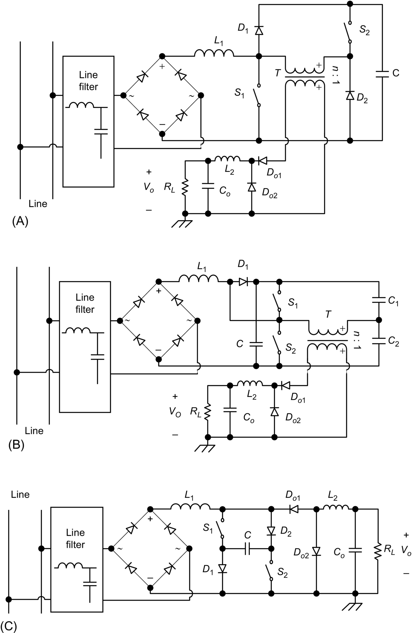

The boost integrated with flyback rectifier/energy storage/dc-dc converter (BIFRED) and boost integrated with buck rectifier/energy storage/dc-dc converter (BIBRED) are two single-stage converters of the integrated high-quality rectifier-regulator (IHQRR) family that have been firstly presented by [103–106]. Both topologies are able to ensure an input current with a low harmonic content and, also, a regulated and isolated output voltage bus using only one switch. The two topologies of BIFRED and BIBRED are designed so that the input inductor and the output inductive element both operate in the DCM mode. It is obvious that BIFRED topology presents a strong similarity with the isolated version of the Sepic converter. Furthermore, the BIBRED topology resembles to the isolated version of the Cuk converter [107]. As it was explained, the two topologies of the BIFRED and BIBRED converters are composed of two integrated converters, where only one switch is used. The BIFRED converter is an integration of a discontinuous conduction mode (DCM) boost converter and a flyback converter. In the BIBRED, the corresponding parts are a DCM boost converter and a forward converter. Schematics of the BIFRED and BIBRED converters are shown in Fig. 16.47A and B, respectively.
Due to the simplicity and low-cost, DCM boost converter is most commonly used for unity PF operation. The main drawback of using boost converter is that it shows considerable distortion of the average line current owing to the slow discharging of the inductor after the switch is turned off [1].
The output DC-DC converter can operate either in DCM or in CCM if small output ripple is desired. If the output circuit operates in CCM, there exists a power unbalance in S4-PFC converter when the load changes. Because the duty ratio is only sensitive to the output voltage in CCM operation, when the output power (output current) decreases, the duty ratio will keep unchanged. As both the input and the output circuit share the power switch, the input circuit will draw an unchanged power from the ac source. As a result, the input power is higher than the output power. The difference between the input power and the output power has to be stored in the storage capacitor, and hence, increase in the dc bus voltage occurs. With the dc bus voltage's rising, the duty ratio decreases. This process will be finished until a new power balance is built. As we can see, the new power balance is achieved at the penalty of increased voltage stress, resulting in high conduction losses in circuit components. Particularly, the high bus voltage causes difficulties in developing S4-converter for universal input (input line voltage rms value from ac 90–260 V) application [1].
Recent research on solving this problem can be found in [108–116]. The circuit in [108] uses two bulk capacitors that share the dc bus voltage change, shown in Fig. 16.48A. As a result, lower voltage is present at each of the capacitor. Ref. [109] proposed a modified boost-forward PFC converter, in which a negative current feedback is introduced to the input circuit by the coupled windings of forward transformer, shown in Fig. 16.48B. In [110], a series resonant circuit called charge pump circuit is introduced into S4-PFC circuit, shown in Fig. 16.48C. As the load decrease, the charge pump circuit can suppress the dc bus voltage automatically [1].
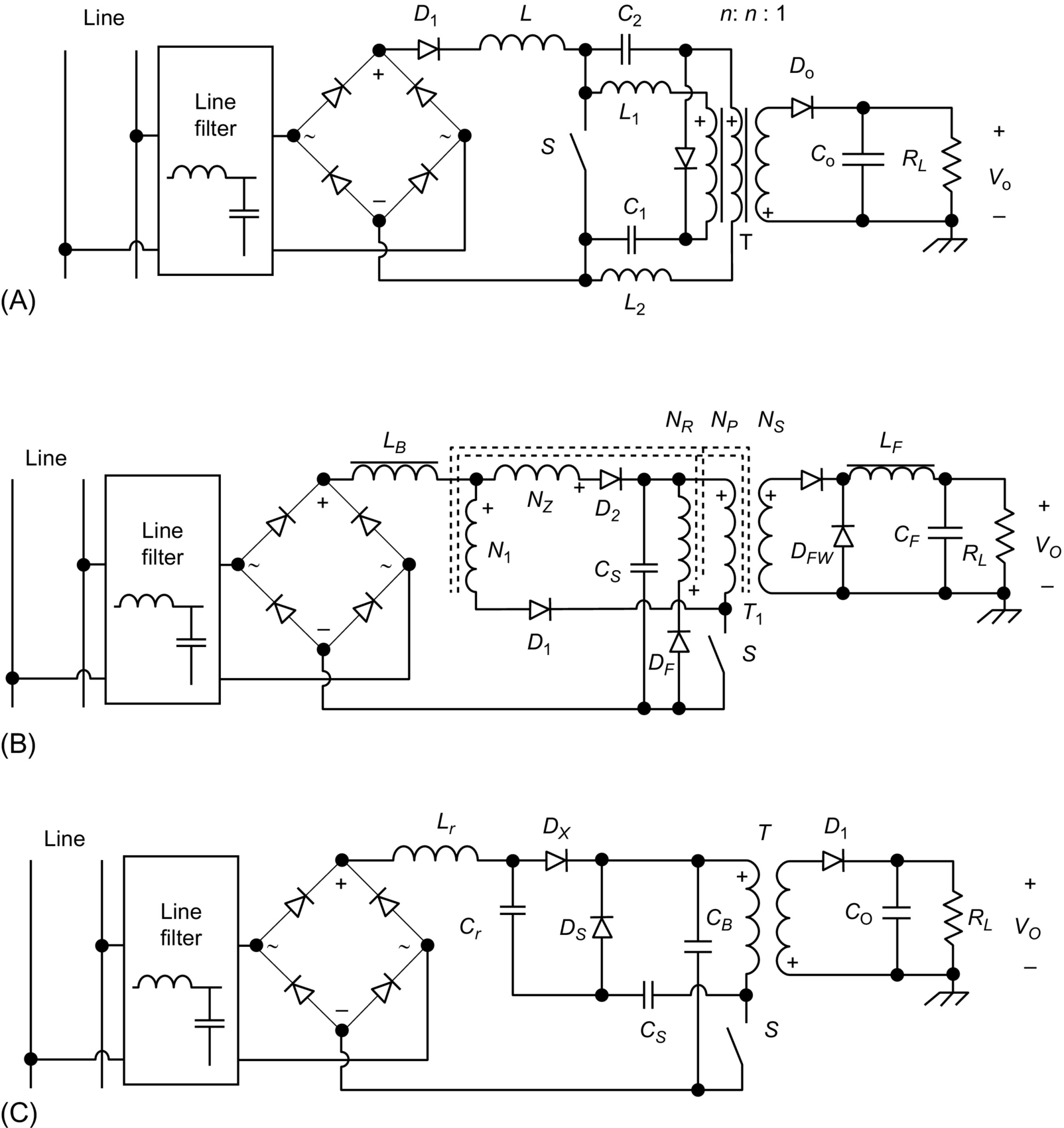
16.5.3 CRM Technique
In this control technique, the switch is turned on when the inductor current falls to zero (when it reaches the time axis), where the switch is kept on for a constant duration during the line cycle and the switch off duration is controlled by a given signal loop. It is clear that the converter operates at the boundary between the continuous and discontinuous current mode (CCM-DCM) [117,118]. It can be said that this type of control is a particular case of hysteretic control in which the lower current command is zero anywhere.
It was proved that the CRM technique has some interesting advantages when it is applied to the boost converter, where the line current is shaped to be sinusoid under COT control [117,119]. Unfortunately, the CRM technique when it is applied to the buck and flyback converters and their derived topologies such as buck-boost, Sepic, and Cuk under COT control leads to a somewhat distorted line current. Hence, the application of CRM technique to these kinds of converters will not allow to meet the PF and THD requirements within the known standards [117,119,120]. To overcome the drawbacks of the CRM control technique, variable on-time (VOT) control technique was proposed and applied to the buck PFC converter [121,122] to achieve high PF and low THD requirement given by the standards. In the same way, based on the input voltage, an improved CRM technique is applied on flyback PFC converter by modulating the turn-on time, However, as the output voltage is not used to modulate the on-time of the switch, when output voltage is varying under constant output current power supply, unity PF is very difficult to be ensured [123]. It is important to clarify that in this control technique, the inductor and switch peak currents are twice the ac system input current peak value. Therefore, the CRM technique is not suitable for high-power applications. However, the CRM technique is attractive in low-power applications such as the PFC for “electronic ballasts” where the following advantages can be achieved: (1) the switch can be easily oversized without increasing cost; (2) the switch operates under zero-current turn-on, avoiding turn-on losses and electromagnetic interference problems; and (3) the smaller sized inductor can be used to reduce the size and cost of the system.
16.5.4 Other PFC Techniques
Extensive research in PFC continues to yield countless new techniques [58,61,124–152]. The research topics are mainly focused on improvements of the PFC circuit performs such as fast performance, high efficiency, low-cost, small input current distortion, and output ripple. The classification of PFC techniques presented here can only cover those methods that are frequently documented in the open literature. There are still many PFC methods that do not fall into the specified categories. The following are some examples [1]:
• Second-harmonic-injected method [126]: In DCM input technique, even the converter operates at constant duty ratio, current distortion still exists. The basic idea of second-harmonic-injected method is compensating the duty ratio by injecting a certain amount of second-harmonic into the duty ratio to modify the input I-V characteristic of the input converter. However, the output voltage may be affected by the modified duty ratio.
• Cycle control technique [127]: It is a new a method recently proposed for harmonics reduction in dc-dc converter that has the simplicity of voltage follower technique. In this technique, a periodic signal proportional to the rectified ac line voltage is used to modulate the duty-cycle of the power switch, where the main goal is to reduce the line current THD and to improve the PF; it offers the following advantages: (1) The generation of the injected signal is based on sensing the output voltage of the bridge rectifier that permits to have a simpler circuit without any additional circuit of phase detecting and phase synchronization, and (2) the modulation index can be used to obtain constant content of harmonics under a wide range of load variation, just with a simple PI controller, and (3) can have a good dynamic behavior under input voltage and load transients.
• Interleaved method [128]: An interleaved PFC circuit composed of several input converters in parallel. The peak input current of these converters follow the line voltage and are interleaved. A sinusoidal total line current is obtained by superimposing all the input current of the converters. The advantage of this method is that the converter input current can be easily smoothed by input EMI filter.
• Waveform synthesis method [129]: This method combines passive and active PFC techniques. Since the rectifier in the passive inductive-input PF corrector has a limited conduction angle, the input current is a single pulse around the peak of the line voltage, whereas the boost converter draws a nonzero current around the zero cross of the line voltage. By controlling the operation mode of the active switch (enable and disable the boost converter at certain line voltage), the waveforms of active and passive PFC circuits are tailored to extend the conduction angle of the rectifier. The resulting current waveform has a PF greater than 0.9 and a THD lower than 20%.
• Digital PFC control technique [130–152]: The digital control of PFC (DPFC) is expected to replace the analog PFC control, especially in medium- and high-power-level applications, due to its several advantages and to the great development in digital circuits. The main advantages of digital PFC control that push and motivate the application of the digital PFC control over other control techniques are mainly summarized in the following points [135]:
a. Reduced sensitivity to circuits' parameter changes.
b. Reduced of analog electronics components.
c. An easy implementation of the controller.
d. An easy adjustment of control parameters.
e. An easy adaptation of the control against the changes of the measured or sensed variables.
f. Digital controller is less expensive compared with the analog controller.
g. Digital controller can be modified easily.
In this chapter, we are not focusing in digital PFC control; however, all the control techniques that have been presented in this chapter in DCM, CCM, and CRM modes can be furthermore extended to digital application for medium- and high-power-level applications (output power range between 200 and 2 kW) when high converter efficiency is desired. As an example, the following digital PFC control techniques have been already investigated:
1. Digital average current mode PFC control (DACM) [135–138]: In this PFC control, the instantaneous sensed variables of the rectified input voltage, the input/inductor current, and the output voltage are digitized. On the other side, a digital PWM (DPWM) is used for the output of the digital-current-loop compensator feeds, a DPWM that generates a discrete time gate driving waveform.
2. Predictive PFC control [139–141]: This control technique allows the computing of the next control value using the current sensed values based on the equations presenting the behavior of the concerned converter to fulfill the requirement of tracking the input reference current shape. The performance of this PFC control is depending on the used sampling frequency; therefore, under high sampling frequency, better result and performance are obtained.
3. Hybrid PFC control [135–146]: This control technique has several advantages that make it a very attractive technique. It is based on combining the digital and the analog techniques, where the analog technique is used for the current loop and the digital technique is used for the voltage loop. The HPFCC gains the merit of both techniques for obtaining improved performances for tracking the input current shape and the desired output voltage under ease and less cost of the hardware implementation, reduced control circuit, rapid dynamic response, and compacted topology.
4. Other digital PFC control techniques [135–152]: All the techniques mentioned in Sections 16.4 and 16.5 can be used under the digital PFC control technique and under the hybrid PFC technique, where in all case the main aim is that the technical advantages and economical advantages have to be respected during the design of the appropriated PFC control technique for the concerned converter topology and the level of the required power.
16.6 Summary
To reduce losses and decrease weight and size associated with converting ac power to dc power in linear power supply, SMPSs were introduced. The high nonlinearity of this kind of power electronic systems that are connected to the power systems supply, handicaps itself by providing the utility power system with low PF and high THD. These unwanted harmonics are commonly corrected by incorporating PFC technique into the SMPS. This chapter gives a technical review of current research in high-frequency PFC, including the definition of PF and THD, configuration of PFC circuit, DCM input technique, CRM technique, and CCM shaping technique. The common issue of these techniques is to properly process the power flow so that the constant power dissipation at the output is reflected into ac power dissipation with two times the line frequency. Technically, PFC techniques encounter the following trade-offs:
(a) Simplicity and accuracy: Single-stage PFC circuit has simple topology and simple control circuit but has less control accuracy, while two-stage PFC circuit has the contrary performance.
(b) Control simplicity and power-handling capability: DCM input technique requires no input current control but has less power-handling capability, while CCM has multiloop control and has more power-handling capability;
(c) Switching frequency and conversion efficiency: To reduce weight and size of the PFC converter, higher switching frequency is desired. However, the associated switching losses result in decrease in conversion efficiency.
(d) Frequency response and bandwidth: To have good dynamic response, wider bandwidth is desired; however, to achieve high PF, bulk storage capacitor and output capacitor have to be used.
In the past decades, research in PFC techniques has led to the development of more efficient circuits and control strategies in order to optimize the design without compromising the above trade-offs. Moreover, since the growth in power electronics strongly relies on the development of semiconductor devices and the recent advent of higher rating power devices, it is believed that the switching-mode PF correctors will completely replace the existing passive reactive compensators in power system. In the distributed power system (DPS) where small size and high efficiency are of extreme importance, a new soft-switching technique has been used in designing PFC circuits. With the ever-increasing market demanding for ultrafast computer, the need for low output voltage (typically less than 1 V) with high output currents and high efficiency converters has never been greater. Research efforts in developing high-frequency high efficiency PFC circuits will continue to grow.