
Average current-mode control of the 12-pulse rectifier
For comparison purposes, a PI-based controller structure is designed (Fig. 35.36B), taking into account that small mismatches of the line voltages or of the trigger angles can completely destroy the current share of the four paralleled rectifiers, in spite of the current equalizing inductances (l and l′). Output voltage control sensing only the output voltage is, therefore, not feasible. Instead, the slow and fast manifold approach is selected. For the fast manifold, four internal current control loops guarantee the same dc current level in each three-phase rectifier and limit the short-circuit currents. For the output slow dynamics, an external cascaded output voltage control loop (Fig. 35.36B), measuring the voltage applied to the load, is the minimum.
For a straightforward design, given the much slower dynamics of the capacitor voltages compared with the input current, the PI current controllers are calculated as shown in Example 35.6, considering the capacitor voltage constant during a switching period and rt≈1 Ω the intrinsic resistance of the transformer windings, thyristor overlap, and inductor l. From Eq. (35.59), Tz=l/rt≈0.044 s. From Eq. (35.62), with the common assumptions, Tp≈0.16 kI s (p=3). These values guarantee a small overshoot (≈5%) and a current rise time of approximately T/3.
To design the external output voltage control loop, each current-controlled rectifier can be considered a voltage-controlled current source iL1(s)/4![]() , since each half-wave rectifier current response will be much faster than the filter output voltage response. Therefore, in the equivalent circuit of Fig. 35.35B, the current source iL1(s)
, since each half-wave rectifier current response will be much faster than the filter output voltage response. Therefore, in the equivalent circuit of Fig. 35.35B, the current source iL1(s)![]() substitutes the input inductor, yielding the transfer function vc2(s)/iL1(s)
substitutes the input inductor, yielding the transfer function vc2(s)/iL1(s)![]() :
:
Vc2(s)iL1(s)=RoC2C1L2Ros3+C1L2s2+(C2Ro+C1Ro)s+1

Given the real pole (p1=−6.7) and two complex poles (p2,3=−6.65±j140.9) of Eq. (35.126), the PI voltage controller zero (1/Tzv=p1) can be chosen with a value equal to the transfer function real pole. The integral gain Tpv can be determined using a root-locus analysis to determine the maximum gain that still guarantees the stability of the closed-loop controlled system. The critical gain for the PI was found to be Tzv/Tpv≈0.4 and then Tpv>0.37. The value Tpv≈2 was selected to obtain weak oscillations, together with almost no overshoot.
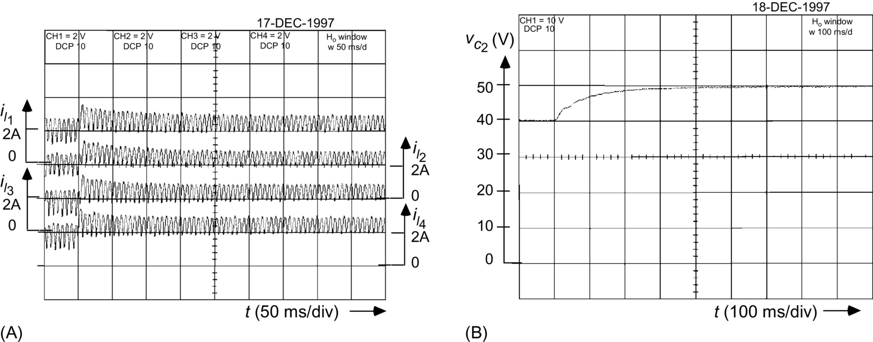
The dynamic and steady-state responses of the output currents of the four rectifiers (il1,il2,il3,il4)![]() and the output voltage Vc2
and the output voltage Vc2![]() were analyzed using a step input from 2 to 2.5 A applied at t=1.1 s, for the currents, and from 40 to 50 V for the Vc2
were analyzed using a step input from 2 to 2.5 A applied at t=1.1 s, for the currents, and from 40 to 50 V for the Vc2![]() voltage. The PI current controllers (Fig. 35.37) show good sharing of the total current, slight overshoot (ζ=0.7), and response time 6.6 ms (T/p).
voltage. The PI current controllers (Fig. 35.37) show good sharing of the total current, slight overshoot (ζ=0.7), and response time 6.6 ms (T/p).
 closed-loop currents and (B) open-loop output voltage Vc2
 .
.The open-loop voltage Vc2![]() presents a rise time of 0.38 s. The PI voltage controller (Fig. 35.38) shows a response time of 0.4 s, no overshoot. The four three-phase half-wave rectifier output currents (il1,il2,il3,andil4)
presents a rise time of 0.38 s. The PI voltage controller (Fig. 35.38) shows a response time of 0.4 s, no overshoot. The four three-phase half-wave rectifier output currents (il1,il2,il3,andil4)![]() present nearly the same transient and steady-state values, with no very high current peaks. These results validate the assumptions made in the PI design.
present nearly the same transient and steady-state values, with no very high current peaks. These results validate the assumptions made in the PI design.
 closed-loop currents and (B) closed output voltage Vc2 and lvc2
 output voltage error.
The closed-loop performance of the fixed-frequency sliding-mode controller (Fig. 35.39) shows that all the il1,il2,il3,andil4![]() currents are almost equal and have peak values only slightly higher than those obtained with the PI linear controllers. The output voltage presents a much faster response time (150 ms) than the PI linear controllers, negligible or no steady-state error, and no overshoot. From these waveforms, it can be concluded that the sliding-mode controller provides a much more effective control of the rectifier, as the output voltage response time is much lower than the obtained with PI linear controllers, without significantly increasing the thyristor currents, overshoots, or costs. Furthermore, sliding mode is an elegant way to know the variables to be measured and to design all the controller and the modulator electronics.
currents are almost equal and have peak values only slightly higher than those obtained with the PI linear controllers. The output voltage presents a much faster response time (150 ms) than the PI linear controllers, negligible or no steady-state error, and no overshoot. From these waveforms, it can be concluded that the sliding-mode controller provides a much more effective control of the rectifier, as the output voltage response time is much lower than the obtained with PI linear controllers, without significantly increasing the thyristor currents, overshoots, or costs. Furthermore, sliding mode is an elegant way to know the variables to be measured and to design all the controller and the modulator electronics.
 closed-loop currents and (B) closed output voltage Vc2 and evc2
 output voltage error.
35.3.5.3 Example 35.13: Sliding-Mode Control of Pulse Width Modulation Audio Power Amplifiers
Linear audio power amplifiers can be astonishing but have efficiencies as low as 15%–20% with speech or music signals. To improve the efficiency of audio systems while preserving the quality, PWM switching power amplifiers, enabling the reduction of the power supply cost, volume, and weight and compensating the efficiency loss of modern loudspeakers, are needed. Moreover, PWM amplifiers can provide a complete digital solution for audio power processing.
For high-fidelity systems, PWM audio amplifiers must present flat passbands of at least 16–20 kHz (±0.5 dB), distortions less than 0.1% at the rated output power, fast dynamic response, and signal-to-noise ratios above 90 dB. This requires fast power semiconductors (usually metal-oxide-semiconductor field-effect transistor (MOSFET) transistors), capable of switching at frequencies near 500 kHz, and fast nonlinear controllers to provide the precise and timely control actions needed to accomplish the mentioned requirements and to eliminate the phase delays in the LC output filter and loudspeakers.
A low-cost PWM audio power amplifier, able to provide over 80 W to 8 Ω loads (Vdd=50 V), can be obtained using a half-bridge power inverter (switching at fPWM≈450 kHz), coupled to an output filter for high-frequency attenuation (Fig. 35.40). A low-sensitivity, doubly terminated passive ladder (double LC), low-pass filter using fourth-order Chebyshev approximation polynomials is selected, given its ability to meet, while minimizing the number of inductors, the following requirements: passband edge frequency 21 kHz, passband ripple 0.5 dB, stopband edge frequency 300 kHz, and 90 dB minimum attenuation in the stopband (L1=80 μH, L2=85 μH, C1=1.7 μF, C2=820 nF, R2=8 Ω, and r1=0.47 Ω).

Modeling the PWM audio amplifier
The two half-bridge switches must always be in complementary states, to avoid power supply internal short circuits. Their state can be represented by the time-dependent variable γ, which is γ=1 when Q1 is on and Q2 is off, and is γ=−1 when Q1 is off and Q2 is on.
Neglecting switch delays, on-state semiconductor voltage drops, and auxiliary networks and supposing small dead times, the half-bridge output voltage (vPWM) is vPWM=γVdd. Considering the state variables and circuit components of Fig. 35.40 and modeling the loudspeaker load as a disturbance represented by the current io (ensuring robustness to the frequency -dependent impedance of the speaker), the switched state-space model of the PWM audio amplifier is
ddt[iL1vc1iL2vo]=[−r1/L1−1/L1001/C10−1/C1001/L20−1/L2001/C20][iL1vc1iL2vo]+[1/L1000000−1/C2][γVddio]

This model will be used to define the output voltage vo controller.
Sliding-mode control of the PWM audio amplifier
The filter output voltage vo, divided by the amplifier gain (1/kv), must follow a reference vor![]() . Defining the output error as evo=vor−kvvo
. Defining the output error as evo=vor−kvvo![]() and also using its time derivatives (eθ, eγ, and eβ) as a new state vector e=[evo,eθ,eγ,eβ]T
and also using its time derivatives (eθ, eγ, and eβ) as a new state vector e=[evo,eθ,eγ,eβ]T![]() , the system equations, in the phase canonical (or controllability) form, can be written in the form
, the system equations, in the phase canonical (or controllability) form, can be written in the form
ddt[evo,eθ,eγ,eβ]T=[eθ,eγ,eβ−f(evo,eθ,eγ,eβ)+pe(t)−γVdd/C1L1C2L2]T

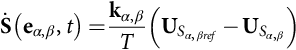
Sliding-mode control of the output voltage will enable a robust and reduced-order dynamics, independent of semiconductors, power supply, filter, and load parameters. According to Eqs. (35.91) and (35.128), the sliding surface is
S(evo,eθ,eγ,eβ,t)=evo+kθeθ+kγeγ+kβeβ=vor−kvvo+kθd(vor−kvvo)dt+kγddt(d(vor−kvvo)dt)+kβddt[ddt(d(vor−kvvo)dt)]=0

In sliding mode, Eq. (35.129) confirms the amplifier gain (vo/vor=1/kv)![]() . To obtain a stable system and the smallest possible response time tr, a pole placement according to a third-order Bessel polynomial is used. Taking tr inversely proportional to a frequency just below the lowest cutoff frequency (ω1) of the double LC filter (tr≈2.8/ω1≈2.8/(2π×21 kHz)≈20 μs) and using Eq. (35.88) with m=3, the characteristic polynomial Eq. (35.130), verifying the Routh-Hurwitz criterion, is obtained:
. To obtain a stable system and the smallest possible response time tr, a pole placement according to a third-order Bessel polynomial is used. Taking tr inversely proportional to a frequency just below the lowest cutoff frequency (ω1) of the double LC filter (tr≈2.8/ω1≈2.8/(2π×21 kHz)≈20 μs) and using Eq. (35.88) with m=3, the characteristic polynomial Eq. (35.130), verifying the Routh-Hurwitz criterion, is obtained:
S(e,s)=1+str+615(str)2+115(str)3
From Eq. (35.97), the switching law for the control input at time tk, γ(tk), must be
γ(tk)=sgn{S(e,tk)+ɛsgn[S(e,tk−1)]}
To ensure reaching and existence conditions, the power supply voltage Vdd must be greater than the maximum required mean value of the output voltage in a switching period Vdd>(¯vPWMmax)![]() . The sliding-mode controller (Fig. 35.41) is obtained from Eqs. (35.129)–(35.131) with kθ=tr, kγ=6t2r/15,kβ=t3r/15
. The sliding-mode controller (Fig. 35.41) is obtained from Eqs. (35.129)–(35.131) with kθ=tr, kγ=6t2r/15,kβ=t3r/15![]() . The derivatives can be approximated by the block diagram of Fig. 35.41B, where h is the oversampling period.
. The derivatives can be approximated by the block diagram of Fig. 35.41B, where h is the oversampling period.
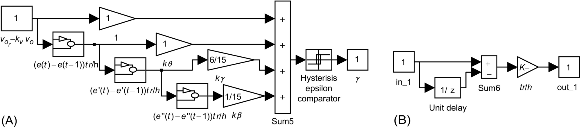
Fig. 35.42A shows the vPWM, vor![]() , vo/10, and error 10×(vor−vo/10)
, vo/10, and error 10×(vor−vo/10)![]() waveforms for a 20 kHz sine input. The overall behavior is much better than the obtained with the sigma-delta controllers (Figs. 35.43 and 35.44) explained below for comparison purposes. There is no 0.5 dB loss or phase delay over the entire audio band; the Chebyshev filter behaves as a maximally flat filter, with higher stopband attenuation. Fig. 35.42B shows vPWM, vor
waveforms for a 20 kHz sine input. The overall behavior is much better than the obtained with the sigma-delta controllers (Figs. 35.43 and 35.44) explained below for comparison purposes. There is no 0.5 dB loss or phase delay over the entire audio band; the Chebyshev filter behaves as a maximally flat filter, with higher stopband attenuation. Fig. 35.42B shows vPWM, vor![]() , and 10×(vor−vo/10)
, and 10×(vor−vo/10)![]() with a 1 kHz square input. There is almost no steady-state error and almost no overshoot on the speaker voltage vo, attesting to the speed of response (t≈20 μs as designed, since, in contrast to Example 35.12, no derivatives were neglected). The stability, the system order reduction, and the sliding-mode controller usefulness for the PWM audio amplifier are also shown.
with a 1 kHz square input. There is almost no steady-state error and almost no overshoot on the speaker voltage vo, attesting to the speed of response (t≈20 μs as designed, since, in contrast to Example 35.12, no derivatives were neglected). The stability, the system order reduction, and the sliding-mode controller usefulness for the PWM audio amplifier are also shown.

 , lower graphs trace 2 show vo/10, and lower graphs trace 3 show 10×(vor−vo/10)
 ): (A) response to a 20 kHz sine input, at 55 W output power, and (B) response to 1 kHz square wave input, at 100 W output power.
 , lower graphs trace 2 shows vo/10, and lower graphs trace 3 show 10×(vor−vo/10)): (A) response to a 20 kHz sine input, at 55 W output power, and (B) response to 1 kHz square wave input, at 100 W output power.
Sigma delta controlled PWM audio amplifier
Assume now the fourth-order Chebyshev low-pass filter, as an ideal filter removing the high-frequency content of the vPWM voltage. Then, the vPWM voltage can be considered as the amplifier output. However, the discontinuous voltage vPWM=γVdd is not a state variable and cannot follow the almost continuous reference vPWMr![]() . The new error variable evPWM=vPWMr−kvγVdd
. The new error variable evPWM=vPWMr−kvγVdd![]() is always far from the zero value. Given this nonzero error, the approach outlined in Section 35.3.4 can be used. The switching law remains Eq. (35.131), but the new control law Eq. (35.132) is
is always far from the zero value. Given this nonzero error, the approach outlined in Section 35.3.4 can be used. The switching law remains Eq. (35.131), but the new control law Eq. (35.132) is
S(evPVM,t)=k∫(vPWMr−kvγVdd)dt=0

The κ parameter is calculated to impose the maximum switching frequency fPWM. Since κ∫1/2fPWM0(vPWMrmax+kvVdd)dt=2ɛ![]() , we obtain
, we obtain
fPWM=κ(vPWMrmax+kvVdd)/4ɛ
Assuming that vPWMr![]() is nearly constant over the switching period 1/fPWM, Eq. (35.132) confirms the amplifier gain, since ¯vPWM=vPWMr/kv
is nearly constant over the switching period 1/fPWM, Eq. (35.132) confirms the amplifier gain, since ¯vPWM=vPWMr/kv![]() .
.
Practical implementation of this control strategy can be done using an integrator with gain κ (κ≈1800) and a comparator with hysteresis ɛ (ɛ≈6 mV) (Fig. 35.43A). Such an arrangement is called a first-order sigma-delta (ΣΔ) modulator.
Fig. 35.44A shows the vPWM, vor, and vo/10 waveforms for a 20 kHz sine input. The overall behavior is as expected, because the practical filter and loudspeaker are not ideal, but notice the 0.5 dB loss and phase delay of the speaker voltage vo, mainly due to the output filter and speaker inductance. In Fig. 35.44B, the vPWM, vor![]() , vo/10, and error 10×(vor−vo/10)
, vo/10, and error 10×(vor−vo/10)![]() for a 1 kHz square input are shown. Note the oscillations and steady-state error of the speaker voltage vo, due to the filter dynamics and double termination.
for a 1 kHz square input are shown. Note the oscillations and steady-state error of the speaker voltage vo, due to the filter dynamics and double termination.
A second-order sigma-delta modulator is a better compromise between circuit complexity and signal-to-quantization noise ratio. As the switching frequency of the two power MOSFET (Fig. 35.40) cannot be further increased, the second-order structure named “cascaded integrators with feedback” (Fig. 35.43B) was selected and designed to eliminate the step response overshoot found in Fig. 35.44B.
Fig. 35.45A, for 1 kHz square input, shows much less overshoot and oscillations than Fig. 35.44B. However, the vPWM, vor![]() , and vo/10 waveforms, for a 20 kHz sine input presented in Fig. 35.45B, show increased output voltage loss, compared to the first-order sigma-delta modulator, since the second-order modulator was designed to eliminate the vo output voltage ringing (therefore reducing the amplifier bandwidth). The obtained performances with these and other sigma-delta structures are inferior to the sliding-mode performances (Fig. 35.42). Sliding mode brings definite advantages as the system order is reduced, flatter passbands are obtained, power supply rejection ratio is increased, and the nonlinear effects, together with the frequency-dependent phase delays, are canceled out.
, and vo/10 waveforms, for a 20 kHz sine input presented in Fig. 35.45B, show increased output voltage loss, compared to the first-order sigma-delta modulator, since the second-order modulator was designed to eliminate the vo output voltage ringing (therefore reducing the amplifier bandwidth). The obtained performances with these and other sigma-delta structures are inferior to the sliding-mode performances (Fig. 35.42). Sliding mode brings definite advantages as the system order is reduced, flatter passbands are obtained, power supply rejection ratio is increased, and the nonlinear effects, together with the frequency-dependent phase delays, are canceled out.

 , lower graphs trace 2 show vo/10, and lower graphs trace 3 show 10×(vor−vo/10)): (A) response to 1 kHz square wave input, at 100 W output power, and (B) response to a 20 kHz sine input, at 55 W output power.
35.3.5.4 Example 35.14: Sliding-Mode Control of Near Unity Power Factor PWM Three Phase Rectifiers
Boost-type voltage-sourced three-phase rectifiers (Fig. 35.46) are multiple-input multiple-output (MIMO) systems capable of bidirectional power flow, near unity power factor operation, and almost sinusoidal input currents and can behave as ac/dc power supplies or power factor compensators.

The fast power semiconductors used (usually MOSFETs or IGBTs) can switch at frequencies much higher than the mains frequency, enabling the voltage controller to provide an output voltage with fast dynamic response.
Modeling the three phase PWM boost rectifier
Neglecting switch delays and dead times, the states of the switches of the kth inverter leg (Fig. 35.46) can be represented by the time-dependent nonlinear variables γk, defined as
γk={1>ifSukisonandSlkisoff0>ifSukisoffandSlkison

Consider the displayed variables of the circuit (Fig. 35.46), where L is the value of the boost inductors, R their resistance, C the value of the output capacitor, and Rc its equivalent series resistance (ESR). Neglecting semiconductor voltage drops, leakage currents, and auxiliary networks, the application of Kirchhoff laws (taking the load current io as a time-dependent perturbation) yields the following switched state-space model of the boost rectifier:
ddt[i1i2i3vo]=[−R/L00(−2γ1+γ2+γ3)/(3L)0−R/L0(−2γ2+γ3+γ1)/(3L)00−R/L(−2γ3+γ1+γ2)/(3L)A41A42A43A44][i1i2i3vo]+[1/L000001/L000001/L00γ1Rc/Lγ2Rc/Lγ3Rc/L−1/C−Rc][v1v2v3iodio/dt]

whereA41=γ1(1C−RRcL),A42=γ2(1C−RRcL),A43=γ3(1C−RRcL),A44=−2Rc(γ1(γ1−γ2)+γ2(γ2−γ3)+γ3(γ3−γ1))3L

Since the input voltage sources have no neutral connection, the preceding model can be simplified, eliminating one equation. Using the relationship (35.136) between the fixed frames x1, 2, 3, and xα,β, in Eq. (35.135), the state-space model (35.137), in the α,β frame, is obtained:
[x1x2]=[√2/30−√1/6√1/2][xαxβ]

ddt[iαiβvo]=[−R/Lω−γα/L0−R/L−γα/LAα31Aα32Aα33][iαiβvo]+[1/L00001/L00γαRc/LγβRc/L−1/C−Rc][vαvβiodio/dt]

whereAα31=γα(1C−RRcL),Aα32=γβ(1C−RRcL),Aα33=−Rc(γ2α+γ2β)L

Sliding-mode control of the PWM rectifier
The model (35.137) is nonlinear and time-variant. Applying the Park transformation (35.138), using a frequency ω rotating reference frame synchronized with the mains (with the q component of the supply voltages equal to zero), the nonlinear, time-invariant model (35.139) is written as
[iαiβ]=[cos(ωt)−sin(ωt)sin(ωt)cos(ωt)][idiq]

ddt[idiqvo]=[−R/Lω−γd/L−ω−R/L−γq/LAd31Ad32Ad33][idiqvo]+[1/L00001/L00γdRc/LγqRc/L−1/C−Rc][vdvqiodiodt]

whereAd31=γd(1C−RRcL),Ad32=γq(1C−RRcL),Ad33=−Rc(γ2d+γ2q)L

This state-space model can be used to obtain the feedback controllers for the PWM boost rectifier. Considering the output voltage vo and the iq current as the controlled outputs and γd and γq the control inputs (MIMO system), the input-output linearization of Eq. (35.72) gives the state-space equations in the controllability canonical form (35.140):
diqdt=−ωid−RLiq−γqLvo+1Lvqdvodt=θ

dθdt=R+Rc(γ2d+γ2q)Lθ−γ2d+γ2qLCvo+γdvd+γqvqLC−RioLC−(1C+RRcL)diodt+ω(1C−RRcL)(γdiq−γdiq)−Rcd2iodt2

where
θ=(1C−RRcL)(γdid+γqiq)−Rc(γ2d+γ2q)Lvo+RcL(γdvd+γqvq)−ioC−Rcdiodt

Using the rectifier overall power balance (from Tellegen's theorem, the converter is conservative, i.e., the power delivered to the load or dissipated in the converter intrinsic devices equals the input power) and neglecting the switching and output capacitor losses, vdid+vqiq=voio+Ri2d![]() . Supposing unity power factor (iqr≈0) and the output vo at steady state, γdid+γqiq≈io,vd=√3VRMS,vq=0,γq≈vq/vo,γd≈(vd−Rid)/vo
. Supposing unity power factor (iqr≈0) and the output vo at steady state, γdid+γqiq≈io,vd=√3VRMS,vq=0,γq≈vq/vo,γd≈(vd−Rid)/vo![]() . Then, from Eqs. (35.140) and (35.91), the following two sliding surfaces can be derived:
. Then, from Eqs. (35.140) and (35.91), the following two sliding surfaces can be derived:
Sq(eiq,t)=keiq(iqr−iq)=0
Sd(evo,eθ,t)≈[β−1(vor−vo)+dvordt+1Cio+Rcdiodt]×LCL−CRRcvo√3VRMS−Rid−id=idr−id=0

where β−1 is the time constant of the desired first-order response of output voltage vo (β≫T>0). For the synthesis of the closed-loop control system, notice that the terms of Eq. (35.142) inside the square brackets can be assumed as the id reference current idr![]() . Furthermore, from Eqs. (35.141) and (35.142), it is seen that the current control loops for id and iq are needed. Considering Eqs. (35.138) and (35.136), the two sliding surfaces can be written as
. Furthermore, from Eqs. (35.141) and (35.142), it is seen that the current control loops for id and iq are needed. Considering Eqs. (35.138) and (35.136), the two sliding surfaces can be written as
Sα(eiα,t)=iαr−iα=0
Sβ(eiβ,t)=iβr−iβ=0
The switching laws relating the sliding surfaces (35.143) and (35.144) with the switching variables γk are
{ifSαβ(eiαβ,t)>ɛtheniαβr>iαβhencechooseγktoincreasetheiαβcurrentifSαβ(eiαβ,t)<−ɛtheniαβr>iαβhencechooseγktodecreasetheiαβcurrent

The practical implementation of this switching strategy could be accomplished using three independent two-level hysteresis comparators. However, this might introduce limit cycles as only two line currents are independent. Therefore, the control laws (35.143) and (35.144) can be implemented using the block diagram of Fig. 35.47A, with d, q/α, and β (from Eq. (35.138)) and 1,2,3/α, and β (from Eq. (35.136)) transformations and two three-level hysteretic comparators with equivalent hysteresis ɛ and ρ to limit the maximum switching frequency. A limiter is included to bound the id reference current to idmax, keeping the input line currents within a safe value. This helps to eliminate the nonminimum-phase behavior (outside sliding mode) when large transients are present while providing short-circuit proof operation.

α, β space vector current modulator
Depending on the values of γk, the bridge rectifier leg output voltages can assume only eight possible distinct states represented as voltage vectors in the α and β reference frame (Fig. 35.47B), for sources with isolated neutral.
With only two independent currents, two three-level hysteresis comparators, for the current errors, must be used in order to accurately select all eight available voltage vectors. Each three-level comparator [16] can be obtained by summing the outputs of two comparators with two levels each. One of these two comparators (δLα and δLβ) has a wide hysteresis width, and the other (δNα and δNβ) has a narrower hysteresis width. The hysteresis bands are represented by ɛ and ρ. Table 35.1 represents all possible output combinations of the resulting four two-level comparators, their sums giving the two three-level comparators (δα and δβ), plus the voltage vector needed to accomplish the current tracking strategy (iα,βr−iα,β)=0![]() (ensuring (iα,βr−iα,β)×d(iα,βr−iα,β)/dt<0
(ensuring (iα,βr−iα,β)×d(iα,βr−iα,β)/dt<0![]() , plus the γk variables and the α and β voltage components).
, plus the γk variables and the α and β voltage components).
From the analysis of the PWM boost rectifier, it is concluded that, if, for example, the voltage vector 2 is applied (γ1=1, γ2=1, and γ3=0), in boost operation, the currents iα and iβ will both decrease. Oppositely, if the voltage vector 5 (γ1=0, γ2=0, and γ3=1) is applied, the currents iα and iβ will both increase. Therefore, vector 2 should be selected when both iα and iβ currents are above their respective references, that is, for δα=−1, δβ=−1, whereas vector 5 must be chosen when both iα and iβ currents are under their respective references or, for δα=1, δβ=1. Nearly all the outputs of Table 35.2 can be filled using this kind of reasoning.
Table 35.2
Two-level and three-level comparator results, showing corresponding vector choice, corresponding γk and vector α and β component voltages; vectors are mapped in Fig. 35.47B
| δLα | δNα | δLβ | δNβ | δα | δβ | Vector | γ1 | γ2 | γ3 | vα | vβ |
| −0.5 | −0.5 | −0.5 | −0.5 | −1 | −1 | 2 | 1 | 1 | 0 | vo/√6 |
vo/√2 |
| 0.5 | −0.5 | −0.5 | −0.5 | 0 | −1 | 2 | 1 | 1 | 0 | vo/√6 |
vo/√2 |
| 0.5 | 0.5 | −0.5 | −0.5 | 1 | −1 | 3 | 0 | 1 | 0 | −vo/√6 |
vo/√2 |
| −0.5 | 0.5 | −0.5 | −0.5 | 0 | −1 | 3 | 0 | 1 | 0 | −vo/√6 |
vo/√2 |
| −0.5 | 0.5 | 0.5 | −0.5 | 0 | 0 | 0 or 7 | 0 or 1 | 0 or 1 | 0 or 1 | 0 | 0 |
| 0.5 | 0.5 | 0.5 | −0.5 | 1 | 0 | 4 | 0 | 1 | 1 | −√2/3vo |
0 |
| 0.5 | −0.5 | 0.5 | −0.5 | 0 | 0 | 0 or 7 | 0 or 1 | 0 or 1 | 0 or 1 | 0 | 0 |
| −0.5 | −0.5 | 0.5 | −0.5 | −1 | 0 | 1 | 1 | 0 | 0 | √2/3vo |
0 |
| −0.5 | −0.5 | 0.5 | 0.5 | −1 | 1 | 6 | 1 | 0 | 1 | vo/√6 |
−vo/√2 |
| 0.5 | −0.5 | 0.5 | 0.5 | 0 | 1 | 6 | 1 | 0 | 1 | vo/√6 |
−vo/√2 |
| 0.5 | 0.5 | 0.5 | 0.5 | 1 | 1 | 5 | 0 | 0 | 1 | −vo/√6 |
−vo/√2 |
| −0.5 | 0.5 | 0.5 | 0.5 | 0 | 1 | 5 | 0 | 0 | 1 | −vo/√6 |
−vo/√2 |
| −0.5 | 0.5 | −0.5 | 0.5 | 0 | 0 | 0 or 7 | 0 or 1 | 0 or 1 | 0 or 1 | 0 | 0 |
| 0.5 | 0.5 | −0.5 | 0.5 | 1 | 0 | 4 | 0 | 1 | 1 | −√2/3vo |
0 |
| 0.5 | −0.5 | −0.5 | 0.5 | 0 | 0 | 0 or 7 | 0 or 1 | 0 or 1 | 0 or 1 | 0 | 0 |
| −0.5 | −0.5 | −0.5 | 0.5 | −1 | 0 | 1 | 1 | 0 | 0 | √2/3vo |
0 |

In the cases where δα=0 and δβ=−1, the vector is selected upon the value of the iα current error (if δLα>0 and δNα<0, then vector 2 and if δLα<0 and δNα>0, then vector 3). When δα=0 and δβ=1, if δLα>0 and δNα<0, then vector 6, else if δLα<0 and δNα>0, then vector 5. The vectors 0 and 7 are selected in order to minimize the switching frequency (if two of the three upper switches are on, then vector 7, otherwise vector 0). The space-vector decoder can be stored in a lookup table (or in an EPROM) whose inputs are the four two-level comparator outputs and the logic result of the operations needed to select between vectors 0 and 7.
PI output voltage control of the current-mode PWM rectifier
Using the α and β current-mode hysteresis modulators to enforce the id and iq currents to follow their reference values, idr,iqr![]() (the values of L and C are such that the id and iq currents usually exhibit a very fast dynamics compared with the slow dynamics of vo), a first-order model (35.146) of the rectifier output voltage can be obtained from Eq. (35.73):
(the values of L and C are such that the id and iq currents usually exhibit a very fast dynamics compared with the slow dynamics of vo), a first-order model (35.146) of the rectifier output voltage can be obtained from Eq. (35.73):
dvodt=(1C−RRcL)(γdidr+γqiqr)−Rc(γ2d+γ2q)Lvo+RcL(γdvd+γqvq)−ioC−Rcdiodt

Assuming now a pure resistor load R1=vo/io and a mean delay Td between the id current and the reference idr![]() , continuous transfer functions result for the id current (id=idr (1+sT d)−1) and for the vo voltage (vo=kAid/(1+skB) with kA and kB obtained from Eq. (35.146)). Therefore, using the same approach as Examples 35.6, 35.8, and 35.11, a linear PI regulator, with gains Kp and Ki (35.147), sampling the error between the output voltage reference vor
, continuous transfer functions result for the id current (id=idr (1+sT d)−1) and for the vo voltage (vo=kAid/(1+skB) with kA and kB obtained from Eq. (35.146)). Therefore, using the same approach as Examples 35.6, 35.8, and 35.11, a linear PI regulator, with gains Kp and Ki (35.147), sampling the error between the output voltage reference vor![]() and the output vo, can be designed to provide a voltage proportional (kI) to the reference current idr(idr=(Kp+Ki/s)KI(vor−vo))
and the output vo, can be designed to provide a voltage proportional (kI) to the reference current idr(idr=(Kp+Ki/s)KI(vor−vo))![]() :
:
Kp=R1+Rc4ζ2TdR1K1γd(1/C−RRc/L)Ki=Rc(γ2d+γ2q)/L+1/(R1C)4ζ2TdK1γd(1/C−RRc/L)

These PI regulator parameters depend on the load resistance R1, on the rectifier parameters (C, Rc, L, and R), on the rectifier operating point γd, on the mean delay time Td, and on the required damping factor ζ. Therefore, the expected response can only be obtained with the nominal load and input voltages, the line current dynamics depending on the Kp and Ki gains.
Results (Fig. 35.48) obtained with the values VRMS≈70 V, L≈1.1 mH, R≈0.1 Ω, C≈2000 μF with equivalent series resistance ESR≈0.1 Ω (Rc≈0.1 Ω), R1≈25 Ω, R2≈12 Ω, β=0.0012, Kp=1.2, Ki=100, and kI=1 show that the α and β space-vector current modulator ensures the current tracking needed (Fig. 35.48) [17–19]. The vo step response reveals a faster sliding-mode controller and the correct design of the current-mode/PI controller parameters. The robustness property of the sliding-mode-controlled output vo, compared with the current mode/PI, is shown in Fig. 35.49.

 and (B) experimental result (1→i1r,2→i2r (10 A/div); 3→i1,4→i2 (5 A/div)).
35.3.5.5 Example 35.15: Sliding-Mode Controllers for Multilevel Inverters
Diode-clamped multilevel inverters (Fig. 35.50) are the converters of choice for high-voltage high-power dc/ac or ac/ac (with dc link) applications, as the active semiconductors (usually gate turn-off thyristors (GTO) or IGBT transistors) of n-level power conversion systems, must withstand only a fraction (normally Ucc/(n−1)) of the total supply voltage Ucc. Moreover, the output voltage of multilevel converters, being staircase-like waveforms with n steps, features lower harmonic distortion compared with the two-level waveforms with the same switching frequency.

The advantages of multilevel converters are paid into the price of the capacitor supply voltage dividers (Fig. 35.51) and voltage equalization circuits, into the cost of extra power supply arrangements (Fig. 35.51C) and into increased control complexity. This example shows how to extend the two-level switching law (35.97) to n-level converters and how to equalize the voltage of the capacitive dividers.

Considering single-phase three-level inverters (Fig. 35.50A), the open-loop control of the output voltage can be made using three-level SPWM. The two-level modulator, seen in Example 35.9, can be easily extended (Fig. 35.52A) to generate the γIII command (Fig. 35.52B) to three-level inverter legs, from the two-level γII signal, either with a dedicated modulator or using the following relation:

γIII=γII(misin(ωt)−sgn(misin(ωt))/2−r(t)/2)−1/2+sgn(misin(ωt))/2

The required three-level SPWM modulators for the output voltage synthesis seldom take into account the semiconductors and the capacitor voltage divider nonideal characteristics. Consequently, the capacitor voltage divider tends to drift, one capacitor being overcharged and the other discharged, and an asymmetry appears in the currents of the power supply. A steady-state error in the output voltage can also be present. Sliding-mode control can provide the optimum switching timing between all the converter levels, together with robustness to supply voltage disturbances, semiconductor nonidealities, and load parameters.
Sliding-mode surface and switching law
For a variable-structure system where the control input ui(t) can present n levels, consider the n values of the integer variable γ, being−(n−1)/2≤γ≤(n−1)/2 and ui(t)=γUcc/(n−1), dependent on the topology and on the conducting semiconductors. To ensure the sliding-mode manifold invariance condition (35.92) and the reaching mode behavior, the switching strategy γ(tk+1) for the time instant tk+1, considering the value of γ(tk), must be
γ(tk+1)={γ(tk)+1ifS(exi,t)>ɛ∧˙S(exi,t)>ɛ∧γ(tk)<(n−1)/2γ(tk)−1ifS(exi,t)<−ɛ∧˙S(exi,t)<−ɛ∧γ(tk)>−(n−1)/2

This switching law can be implemented as depicted in Fig. 35.53A and for five levels in B. An alternative is shown in Fig. 35.53C and named stability condition-based modulator [20], where the switching law (35.149) is directly used, calculating the sliding-mode surface and its time derivative, implemented as a discrete time variation. They are two-level quantized, and upon their values (obtained by half of their sum), the voltage level is increased (or decreased), until it reaches the maximum (or the minimum). Therefore, the output level is increased (or decreased) if the error and its derivative are both positive (or negative), with the upper limit λmáx=(n−1)/2 and lower limit λmin=−(n−1)/2.

Other implementations are possible (Fig. 35.53D), since in every modulation method the generated pulse levels must have the same volt-second average of the fundamental sinusoidal (i.e., the integral over time of the n-level voltage waveform minus the value of the fundamental should be zero).
Control of the output voltage in single-phase multilevel converters
To control the inverter output voltage, in closed-loop and in diode-clamped multilevel inverters with n levels and supply voltage Ucc, a control law similar to Eq. (35.132), S(euo,t)=κ∫(uor−kvγ(tk)Ucc/(n−1))dt=0![]() , is suitable.
, is suitable.
Fig. 35.54A shows the waveforms of a five-level sliding-mode-controlled inverter, namely, the input sinus voltage, the generated output staircase wave, and the sliding-surface instantaneous error. This error is always within a band centered around the zero value and presents zero mean value, which is not the case of sigma-delta modulators followed by n-level quantizers, where the error presents an offset mean value in each half period.

 , the generated output staircase wave uo, and the value of the sliding surface S(exi,t)
 ; (B) scaled waveforms of a three-level neutral-point-clamped inverter showing the capacitor voltage unbalance (shown as two near-flat lines touching the tips of the PWM pulses); and (C) experimental results from a laboratory prototype of a three-level single-phase power inverter with the capacitor voltage equalization described.
Experimental multilevel converters always show capacitor voltage unbalances (Fig. 35.54B) due to small differences between semiconductor voltage drops and circuitry offsets. To obtain capacitor voltage equalization, the voltage error (vc2−Ucc/2)![]() is fed back to the controller (Fig. 35.55A) to counteract the circuitry offsets. Experimental results (Fig. 35.54C) clearly show the effectiveness of the correction made. The small steady-state error, between the voltages of the two capacitors, still present, could be eliminated using an integral regulator (Fig. 35.55B).
is fed back to the controller (Fig. 35.55A) to counteract the circuitry offsets. Experimental results (Fig. 35.54C) clearly show the effectiveness of the correction made. The small steady-state error, between the voltages of the two capacitors, still present, could be eliminated using an integral regulator (Fig. 35.55B).

Fig. 35.56 confirms the robustness of the sliding-mode controller to power supply disturbances.
 input, (B) PWM output voltage uo, and (C) the integral of the error voltage, which is maintained close to zero.
Output current control in single-phase multilevel converters
Considering an inductive load with current iL, the control law (35.107) and the switching law of (35.149) should be used for single-phase multilevel inverters. Results obtained using the capacitor voltage equalization principle just described are shown in Fig. 35.57.

35.3.5.6 Example 35.16: Sliding-Mode Controllers for Three-Phase Multilevel Inverters
Three-phase n-level inverters (Fig. 35.58) are suitable for high-voltage, high-power dc/ac applications, such as modern high-speed railway traction drives, as the controlled turn-off semiconductors must block only a fraction (normally Udc/(n−1)) of the total supply voltage Udc.

This example presents a real-time modulator for the control of the three output voltages and capacitor voltage equalization, based on the use of sliding mode and space vectors represented in the α and β frame. Capacitor voltage equalization is done with the proper selection of redundant space vectors.
Output voltage control in multilevel converters
To guarantee the topological constraints of this converter and the correct sharing of the Udc voltage by the semiconductors, the switching strategy for the k leg (k∈{1, 2, 3}) must ensure complementary states to switches Sk1 and Sk3. The same restriction applies for Sk2 and Sk4. Neglecting switching delays, dead times, on-state semiconductor voltage drops, snubber networks, and power supply variations; supposing small dead times and equal capacitor voltages UC1=UC2=Udc/2; and using the time-dependent switching variable γk(t), the leg output voltage Uk (Fig. 35.58) will be Uk=γk(t)Udc/2, with
γk(t)={1ifSk1∧Sk2areON∧Sk3∧Sk4areOFF0ifSk2∧Sk3areON∧Sk1∧Sk4areOFF−1ifSk3∧Sk4areON∧Sk1∧Sk2areOFF

The converter output voltages USk of vector US can be expressed as
US=[2/3−1/3−1/3−1/32/3−1/3−1/3−1/32/3][γ1γ2γ3]Udc2

The application of the Concordia transformation US1,2,3=[C] USα, β, o (Eq. (35.152) to (35.151))
[US1US2US3]=√23[101/√2−1/2√3/21/√2−1/2−√3/21/√2][USαUSβUSo]

gives the output voltage vector in the α and β coordinates USα,β![]() :
:
USα,β=[UsαUsβ]=√23[1−12−120√32−√32][Γ1Γ2Γ3]Udc2=[ΓαΓβ]Udc2

where
Γ1=23γ1−13γ2−13γ3;Γ2=23γ2−13γ3−13γ1;Γ3=23γ3−13γ1−13γ2

The output voltage vector in the α and β coordinates USα,β![]() is discontinuous. A suitable state variable for this output can be its average value ˉUSα,β
is discontinuous. A suitable state variable for this output can be its average value ˉUSα,β![]() during one switching period:
during one switching period:
ˉUSα,β=1T∫T0USα,βdt=1T∫T0Γα,βUdc2dt

The controllable canonical form is
ddtˉUSα,β=USα,βT=Γα,βTUdc2

Considering the control goal ˉUSα,β=ˉUSα,βref![]() and Eq. (35.91), the sliding surface is
and Eq. (35.91), the sliding surface is
S(eα,β,t)=φ∑o=1kαβoeα,βo=kα,β1eα,β1=kα,β1(ˉUSα,βref−ˉUSα,β)=kα,βT∫T0(USα,βref−USα,β)dt=0

To ensure reaching mode behavior and sliding-mode stability (35.92), as the first derivative of Eq. (35.157), ˙S(eα,β,t)![]() is
is
˙S(eα,β,t)=kα,βT(USα,βref−USα,β)
The switching law is
S(eα,β,t)>0⇒˙S(eα,β,t)<0⇒USα,β>USα,βrefS(eα,β,t)<0⇒˙S(eα,β,t)>0⇒USα,β<USα,βref

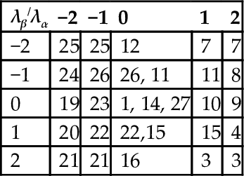
This switching strategy must select the proper values of USα,β![]() from the available outputs. As each inverter leg (Fig. 35.58) can deliver one of the three possible output voltages (Udc/2, 0, and−Udc/2), all the 27 possible output voltage vectors listed in Table 35.3 can be represented in the α and β frame of Fig. 35.59 (in per units, 1 p.u. = Udc). There are nine different levels for the α space vector component and only five for the β component. However, considering any particular value of α (or β) component, there are at most five levels available in the remaining orthogonal component. From the load viewpoint, the 27 space vectors of Table 35.3 define only 19 distinct space positions (Fig. 35.59).
from the available outputs. As each inverter leg (Fig. 35.58) can deliver one of the three possible output voltages (Udc/2, 0, and−Udc/2), all the 27 possible output voltage vectors listed in Table 35.3 can be represented in the α and β frame of Fig. 35.59 (in per units, 1 p.u. = Udc). There are nine different levels for the α space vector component and only five for the β component. However, considering any particular value of α (or β) component, there are at most five levels available in the remaining orthogonal component. From the load viewpoint, the 27 space vectors of Table 35.3 define only 19 distinct space positions (Fig. 35.59).

Table 35.3
Vectors of the three-phase three-level converter, switching variables γk, switch states skj, and the corresponding output voltages, line to neutral point, line to line, and α and β components in per units
| Vector | γ1 | γ2 | γ3 | S11 | S12 | S13 | S14 | S21 | S22 | S23 | S24 | S31 | S32 | S33 | S34 | U1 | U2 | U3 | U12 | U23 | U31 | Usα/Udc | Usβ/Udc |
| 1 | 1 | 1 | 1 | 1 | 1 | 0 | 0 | 1 | 1 | 0 | 0 | 1 | 1 | 0 | 0 | Udc/2 | Udc/2 | Udc/2 | 0 | 0 | 0 | 0.00 | 0.00 |
| 2 | 1 | 1 | 0 | 1 | 1 | 0 | 0 | 1 | 1 | 0 | 0 | 0 | 1 | 1 | 0 | Udc/2 | Udc/2 | 0 | 0 | Udc/2 | −Udc/2 | 0.20 | 0.35 |
| 3 | 1 | 1 | −1 | 1 | 1 | 0 | 0 | 1 | 1 | 0 | 0 | 0 | 0 | 1 | 1 | Udc/2 | Udc/2 | −Udc/2 | 0 | Udc | −Udc | 0.41 | 0.71 |
| 4 | 1 | 0 | −1 | 1 | 1 | 0 | 0 | 0 | 1 | 1 | 0 | 0 | 0 | 1 | 1 | Udc/2 | 0 | −Udc/2 | Udc/2 | Udc/2 | −Udc | 0.61 | 0.35 |
| 5 | 1 | 0 | 0 | 1 | 1 | 0 | 0 | 0 | 1 | 1 | 0 | 0 | 1 | 1 | 0 | Udc/2 | 0 | 0 | Udc/2 | 0 | −Udc/2 | 0.41 | 0.00 |
| 6 | 1 | 0 | 1 | 1 | 1 | 0 | 0 | 0 | 1 | 1 | 0 | 1 | 1 | 0 | 0 | Udc/2 | 0 | Udc/2 | Udc/2 | −Udc/2 | 0 | 0.20 | −0.35 |
| 7 | 1 | −1 | 1 | 1 | 1 | 0 | 0 | 0 | 0 | 1 | 1 | 1 | 1 | 0 | 0 | Udc/2 | −Udc/2 | Udc/2 | Udc | −Udc | 0 | 0.41 | −0.71 |
| 8 | 1 | −1 | 0 | 1 | 1 | 0 | 0 | 0 | 0 | 1 | 1 | 0 | 1 | 1 | 0 | Udc/2 | −Udc/2 | 0 | Udc | −Udc/2 | −Udc/2 | 0.61 | −0.35 |
| 9 | 1 | −1 | −1 | 1 | 1 | 0 | 0 | 0 | 0 | 1 | 1 | 0 | 0 | 1 | 1 | Udc/2 | −Udc/2 | −Udc/2 | Udc | 0 | −Udc | 0.82 | 0.00 |
| 10 | 0 | −1 | −1 | 0 | 1 | 1 | 0 | 0 | 0 | 1 | 1 | 0 | 0 | 1 | 1 | 0 | −Udc/2 | −Udc/2 | Udc/2 | 0 | −Udc/2 | 0.41 | 0.00 |
| 11 | 0 | −1 | 0 | 0 | 1 | 1 | 0 | 0 | 0 | 1 | 1 | 0 | 1 | 1 | 0 | 0 | −Udc/2 | 0 | Udc/2 | −Udc/2 | 0 | 0.20 | −0.35 |
| 12 | 0 | −1 | 1 | 0 | 1 | 1 | 0 | 0 | 0 | 1 | 1 | 1 | 1 | 0 | 0 | 0 | −Udc/2 | Udc/2 | Udc/2 | −Udc | Udc/2 | 0.00 | −0.71 |
| 13 | 0 | 0 | 1 | 0 | 1 | 1 | 0 | 0 | 1 | 1 | 0 | 1 | 1 | 0 | 0 | 0 | 0 | Udc/2 | 0 | −Udc/2 | Udc/2 | −0.20 | −0.35 |
| 14 | 0 | 0 | 0 | 0 | 1 | 1 | 0 | 0 | 1 | 1 | 0 | 0 | 1 | 1 | 0 | 0 | 0 | 0 | 0 | 0 | 0 | 0.00 | 0.00 |
| 15 | 0 | 0 | −1 | 0 | 1 | 1 | 0 | 0 | 1 | 1 | 0 | 0 | 0 | 1 | 1 | 0 | 0 | −Udc/2 | 0 | Udc/2 | −Udc/2 | 0.20 | 0.35 |
| 16 | 0 | 1 | −1 | 0 | 1 | 1 | 0 | 1 | 1 | 0 | 0 | 0 | 0 | 1 | 1 | 0 | Udc/2 | −Udc/2 | −Udc/2 | Udc | −Udc/2 | 0.00 | 0.71 |
| 17 | 0 | 1 | 0 | 0 | 1 | 1 | 0 | 1 | 1 | 0 | 0 | 0 | 1 | 1 | 0 | 0 | Udc/2 | 0 | −Udc/2 | Udc/2 | 0 | −0.20 | 0.35 |
| 18 | 0 | 1 | 1 | 0 | 1 | 1 | 0 | 1 | 1 | 0 | 0 | 1 | 1 | 0 | 0 | 0 | Udc/2 | Udc/2 | −Udc/2 | 0 | Udc/2 | −0.41 | 0.00 |
| 19 | −1 | 1 | 1 | 0 | 0 | 1 | 1 | 1 | 1 | 0 | 0 | 1 | 1 | 0 | 0 | −Udc/2 | Udc/2 | Udc/2 | −Udc | 0 | Udc | −0.82 | 0.00 |
| 20 | −1 | 1 | 0 | 0 | 0 | 1 | 1 | 1 | 1 | 0 | 0 | 0 | 1 | 1 | 0 | −Udc/2 | Udc/2 | 0 | −Udc | Udc | Udc/2 | −0.61 | 0.35 |
| 21 | −1 | 1 | −1 | 0 | 0 | 1 | 1 | 1 | 1 | 0 | 0 | 0 | 0 | 1 | 1 | −Udc/2 | Udc/2 | −Udc/2 | −Udc | Udc | 0 | −0.41 | 0.71 |
| 22 | −1 | 0 | −1 | 0 | 0 | 1 | 1 | 0 | 1 | 1 | 0 | 0 | 0 | 1 | 1 | −Udc/2 | 0 | −Udc/2 | −Udc/2 | Udc/2 | 0 | −0.20 | 0.35 |
| 23 | −1 | 0 | 0 | 0 | 0 | 1 | 1 | 0 | 1 | 1 | 0 | 0 | 1 | 1 | 0 | −Udc/2 | 0 | 0 | −Udc/2 | 0 | Udc/2 | −0.41 | 0.00 |
| 24 | −1 | 0 | 1 | 0 | 0 | 1 | 1 | 0 | 1 | 1 | 0 | 1 | 1 | 0 | 0 | −Udc/2 | 0 | Udc/2 | −Udc/2 | −Udc/2 | Udc | −0.61 | −0.35 |
| 25 | −1 | −1 | 1 | 0 | 0 | 1 | 1 | 0 | 0 | 1 | 1 | 1 | 1 | 0 | 0 | −Udc/2 | −Udc/2 | Udc/2 | 0 | −Udc/2 | Udc | −0.41 | −0.71 |
| 26 | −1 | −1 | 0 | 0 | 0 | 1 | 1 | 0 | 0 | 1 | 1 | 0 | 1 | 1 | 0 | −Udc/2 | −Udc/2 | 0 | 0 | −Udc/2 | Udc/2 | −0.20 | −0.35 |
| 27 | −1 | −1 | −1 | 0 | 0 | 1 | 1 | 0 | 0 | 1 | 1 | 0 | 0 | 1 | 1 | −Udc/2 | −Udc/2 | −Udc/2 | 0 | 0 | 0 | 0.00 | 0.00 |

To select one of these 19 positions from the control law (35.157) and the switching law of Eq. (35.159), two five-level hysteretic comparators (Fig. 35.53B) must be used (52=25). Their outputs are the integer variables λα and λβ, denoted λα, β (λα, λβ∈{−2; −1; 0; 1; 2}) corresponding to the five selectable levels of Γα and Γβ. Considering the sliding-mode stability, λα, β, at time step j+1, is given by Eq. (35.160), knowing their previous values at step j. This means that the output level is increased (decreased) if the error and its derivative are both positive (negative), provided the maximum (minimum) output level is not exceeded:
{(λα,β)j+1=(λα,β)j+1ifS(eα,β,t)>ɛ∧˙S(eα,β,t)>ɛ∧(λα,β)j<2(λα,β)j+1=(λα,β)j−1ifS(eα,β,t)<−ɛ∧˙S(eα,β,t)<−ɛ∧(λα,β)j>−2

The available space vectors must be chosen not only to reduce the mean output voltage errors but also to guarantee transitions only between the adjacent levels, to minimize the capacitor voltage unbalance, to minimize the switching frequency, to observe minimum on or off times if applicable, and to equally stress all the semiconductors.
Using Eq. (35.160) and the control laws S(eα, β, t) Eq. (35.157), Tables 35.4 and 35.5 can be used to choose the correct voltage vector in order to ensure stability, output voltage tracking, and DC capacitor voltage equalization. The vector with α and β components corresponding to the levels of the pair λβ and λα is selected, provided that the adjacent transitions on inverter legs are obtained. If there is no directly corresponding vector, then the nearest vector guaranteeing adjacent transitions is selected. If a zero vector must be applied, then one of the three zero vectors (1, 14, and 27) is selected, to minimize the switching frequency. If more than one vector is the nearest, then one of them is selected to equalize the capacitor voltages, as shown next.

DC capacitor voltage equalization
The discrete values of λα, β allow 25 different combinations. As only 19 are distinct from the load viewpoint, the extra ones can be used to select vectors that are able to equalize the capacitor voltages (UC1=UC2=Udc/2).
Considering the control goal UC1=UC2, since the first derivatives of UC1 and UC2 Eq. (35.161) directly depend on the γk(t) control inputs, from Eq. (35.91), the sliding surface is given by Eq. (35.162), where kU is a positive gain:
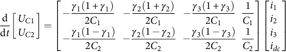
ddt[UC1UC2]=[−γ1(1+γ1)2C1−γ2(1+γ2)2C1−γ3(1+γ3)2C11C1−γ1(1−γ1)2C2−γ2(1−γ2)2C2−γ3(1−γ3)2C21C2][i1i2i3idc]
S(eUc,t)=kUeUc(t)=kU(UC1–UC2)=0
The first derivative of UC1−UC2 (the sliding surface) is (Fig. 35.58 with C1=C2=C)
ddteUc=iC1C1−iC2C2=inC=(γ23−γ21)i1+(γ23−γ22)i2C
To ensure reaching mode behavior and sliding-mode stability, from Eq. (35.92), considering a small enough eUc (t) error, ɛeU, the switching law is
S(eUc,t)>ɛeU⇒˙S(eUc,t)<0⇒in<0S(eUc,t)<−ɛeU⇒˙S(eUc,t)>0⇒in>0

From circuit analysis, it can be seen that vectors (2, 5, 6, 13, 17, and 18) result in the discharge of capacitor C1, if the converter operates in inverter mode, or in the charge of C1, if the converter operates in boost rectifier (regenerative) mode. Similar reasoning can be applied for vectors (10, 11, 15, 22, 23, and 26) and capacitor C2, since this vector set gives in currents with opposite sign relatively to the set (2, 5, 6, 13, 17, and 18). Therefore, considering the vector [Υ1,Υ2]=[(γ21−γ23),(γ22−γ23)]![]() , the switching law is the following:
, the switching law is the following:
If (UC1 – UC2)>ɛeU,
THEN{IFthecandidatevectorfrom{2,5,6,13,17,18}gives(Υ1i1+Υ2i2)>0,THENchoosethevectoraccordingtoλα,βonTable34.4;ELSE,thecandidatevectorof{10,11,15,22,23,26}gives(Υ1i1+Υ2i2)>0,thevectorbeingchosenaccordingtoλα,βfrom(table34.5)

If (UC1 – UC2)<ɛeU,
THEN{IFthecandidatevectorfrom{2,5,6,13,17,18}gives(Υ1i1+Υ2i2)<0,THENchoosethevectoraccordingtoλα,βonTable34.4;ELSE,thecandidatevectorof{10,11,15,22,23,26}gives(Υ1i1+Υ2i2)<0,thevectorbeingchosenaccordingtoλα,βfrom(table34.5)

For example, consider the case where UC1>UC2+ɛeU. Then, the capacitor C2 must be charged, and Table 35.4 must be used if the multilevel inverter is operating in the inverter mode or Table 35.5 for the regenerative mode. Additionally, when using Table 35.4, if λα=−1 and λβ=−1, then vector 13 should be used.
Experimental results shown in Fig. 35.61 were obtained with a low-power, scaled-down laboratory prototype (150 V and 3 kW) of a three-level inverter (Fig. 35.60), controlled by two four-level comparators, and described capacitor voltage equalizing procedures and EPROM-based lookup Tables 35.3–35.5. Transistors IGBT (MG25Q2YS40) were switched at frequencies near 4 kHz, with neutral clamp diodes 40HFL, C1≈C2≈20 mF. The load was mainly inductive (3×10 mH and 2 Ω).


The inverter number of levels (three for the phase voltage and five for the line voltage), together with the adjacent transitions of inverter legs between levels, is shown in Fig. 35.61A and, in detail, in Fig. 35.62A.
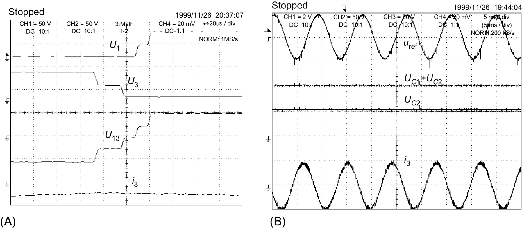
The performance of the capacitor voltage equalizing strategy is shown in Fig. 35.62B, where the reference current of phase 1 and the output current of phase 3, together with the power supply voltage (Udc≈100 V) and the voltage of capacitor C2(UC2), can be seen. It can be noted that the UC2 voltage is nearly half of the supply voltage. Therefore, the capacitor voltages are nearly equal. Furthermore, it can be stated that without this voltage equalization procedure, the three-level inverter operates only during a brief transient, during which one of the capacitor voltages vanishes to nearly 0 V and the other is overcharged to the supply voltage. Fig. 35.61B shows the harmonic spectrum of the output voltages, where the harmonics due to the switching frequency (≈4.5 kHz) and the fundamental harmonic can be seen.
On-line output current control in multilevel inverters
Considering a standard inductive balanced load (R and L) with electromotive force (u) and isolated neutral, the converter output currents ik can be expressed:
USk=Rik+Ldikdt+uek

Now analyzing the circuit of Fig. 35.58, the multilevel converter switched state-space model can be obtained:
ddt[i1i2i3]=−[RL000RL000RL][i1i2i3]−[1L0001L0001L][ue1ue2ue3]+[Γ1LΓ2LΓ3L]Udc2

The application of the Concordia matrix Eqs. (35.152)–(35.166) reduces the number of the new model equations (Eq. (35.167)) to two, since an isolated neutral is assumed:
ddt[iαiβ]=−[RL00RL][iαiβ]−[1L001L][ueαueβ]+[1L001L][USαUSβ]

The model Eq. (35.167) of this multiple-input multiple-output system (MIMO) with outputs iα and iβ reveals the control inputs USα and USβ, dependent on the control variables γk(t).
From Eqs. (35.167) and (35.91), the two sliding surfaces S(eα, β, t) are
S(eα,β,t)=kα,β(iα,βref–iα,β)=kα,βeα,β=0
The first derivatives of Eq. (35.167), denoted ˙S(eα,β,t)![]() , are
, are
˙S(eα,β,t)=kα,β(˙iα,βref−˙iα,β)=kα,β[˙iα,βref+RL−1iα,β+ueα,βL−1−USα,βL−1]

Therefore, the switching law is
S(eα,β,t)>0⇒˙S(eα,β,t)<0⇒USα,β>L˙iα,βref+Riα,β+ueα,βS(eα,β,t)<0⇒˙S(eα,β,t)>0⇒USα,β>L˙iα,βref+Riα,β+ueα,β

These switching laws are implemented using the same α and β vector modulator described above in this example.
Fig. 35.63A shows the experimental results. The multilevel converter and proposed control behavior are obtained for step inputs (4–2 A) in the amplitude of the sinus references with frequency near 52 Hz (Udc≈150 V). Observe the tracking ability, the fast transient response, and the balanced three-phase currents. Fig. 35.63B shows almost the same test (step response from 2 to 4 A at the same frequency), but now, the power supply is set at 50 V, and the inductive load was unbalanced (±30% on resistor value). The response remains virtually the same, with tracking ability, almost no current distortions due to dead times or semiconductor voltage drops. These results and other works [21,51] confirm experimentally that the designed controllers are robust concerning these nonidealities.
