Thyristors
Tanya K. Gachovska Senior Verification Engineer, Solantro Semiconductor Corp, Ottawa, ON, Canada
Jerry L. Hudgins University of Nebraska-Lincoln, Lincoln, NE, United States
Angus Bryant System Architect Amantys Power Electronics Ltd, Cambridge, UK
Patrick Palmer University of Cambridge, Cambridge, UK
Subbaraya Yuvarajan North Dakota State University, Fargo, ND, United States
Abstract
Thyristors are usually three-terminal devices that have four layers of alternating p-type and n-type material (i.e., three p-n junctions) comprising its main power handling section. In contrast to the linear relation that exists between load and control currents in a transistor, the thyristor is bistable. The control terminal of the thyristor, called the gate (G) electrode, may be connected to an integrated and complex structure as a part of the device. The other two terminals, called the anode (A) and cathode (K), handle the large applied potentials (often of both polarities) and conduct the major current through the thyristor. The anode and cathode terminals are connected in series with the load to which power is to be controlled.
Keywords
Thyristor; SCR; GTO; MOS-controlled thyristors; Static induction thyristors; Optical triggered thyristors; BY-directional controlled thyristors: Diac; Triac
3.1 Introduction
Thyristors are usually three-terminal devices that have four layers of alternating p-type and n-type material (i.e., three p-n junctions) comprising its main power handling section. In contrast to the linear relation that exists between load and control currents in a transistor, the thyristor is bistable. The control terminal of the thyristor, called the gate (G) electrode, may be connected to an integrated and complex structure as a part of the device. The other two terminals, called the anode (A) and cathode (K), handle the large applied potentials (often of both polarities) and conduct the major current through the thyristor. The anode and cathode terminals are connected in series with the load to which power is to be controlled.
Thyristors are used to approximate ideal closed (no voltage drop between anode and cathode) or open (no anode current flow) switches for control of power flow in a circuit. This differs from low-level digital switching circuits that are designed to deliver two distinct small voltage levels while conducting small currents (ideally zero). Thyristor circuits must have the capability of delivering large currents and be able to withstand large externally applied voltages. All thyristor types are controllable in switching from a forward-blocking state (positive potential applied to the anode with respect to the cathode, with correspondingly little anode current flow) into a forward-conduction state (large forward anode current flowing, with a small anode-cathode potential drop). Most thyristors have the characteristic that after switching from a forward-blocking state into the forward-conduction state, the gate signal can be removed and the thyristor will remain in its forward-conduction mode. This property is termed “latching” and is an important distinction between thyristors and other types of power electronic devices. Some thyristors are also controllable in switching from forward-conduction back to a forward-blocking state. The particular design of a thyristor will determine its controllability and often its application.
Thyristors are typically used at the highest energy levels in power-conditioning circuits because they are designed to handle the largest currents and voltages of any device technology (systems approximately with voltages above 1 kV or currents above 100 A). Many medium-power circuits (systems operating at less than 1 kV or 100 A) and particularly low-power circuits (systems operating below 100 V or several amperes) generally make use of power bipolar transistors, power metal-oxide-semiconductor field-effect transistors (MOSFETs), or insulated gate bipolar transistors (IGBTs) as the main switching elements because of the relative ease in controlling them. IGBT technology, however, continues to improve and multiple silicon die are commonly packaged together in a module. These modules are replacing thyristors in applications operating up to 3 kV that require controllable turn-off because of easier gate-drive requirements. Power diodes are used throughout all levels of power-conditioning circuits and systems for component protection and wave shaping.
A thyristor used in some ac power circuits (50 or 60 Hz in commercial utilities or 400 Hz in aircraft) to control ac power flow can be made to optimize internal power loss at the expense of switching speed. These thyristors are called phase-control devices, because they are generally turned from a forward-blocking into a forward-conducting state at some specified phase angle of the applied sinusoidal anode-cathode voltage waveform. A second class of thyristors is used in association with dc sources or in converting ac power at one amplitude and frequency into ac power at another amplitude and frequency and must generally switch on and off relatively quickly. A typical application for the second class of thyristors is in converting a dc voltage or current into an ac voltage or current. A circuit that performs this operation is often called an inverter, and the associated thyristors used are referred to as inverter thyristors.
There are four major types of thyristors: (i) the silicon-controlled rectifier (SCR), (ii) the gate turn-off thyristor (GTO) and its close relative the integrated gate-commutated thyristor (IGCT), (iii) the MOS-controlled thyristor (MCT) and its various forms, and (iv) the static induction thyristor (SITh). MCTs are so-named because many parallel enhancement-mode, MOSFET structures of one charge type are integrated into the thyristor for turn-on, and many more MOSFETs of the other charge types are integrated into the thyristor for turn-off. An SITh or field-controlled thyristor (FCTh) has essentially the same construction as a power diode with a gate structure that can pinch-off anode current flow. Although MCTs, derivative forms of the MCT and SIThs, have the advantage of being essentially voltage-controlled devices (i.e., little control current is required for turn-on or turnoff and therefore require simplified control circuits attached to the gate electrode), they are currently only found in niche applications such as pulse power. Detailed discussion of variations of MCTs and SIThs and additional references on these devices are discussed by Hudgins in [1]. Other types of thyristors include the triac (a pair of antiparallel SCRs integrated together to form a bidirectional current switch) and the programmable unijunction transistor (PUT).
The SCRs and GTOs are designed to operate at all power levels. These devices are primarily controlled using electric signals (current), though some types are made to be controlled using optical energy (photons) for turn-on. Subclasses of SCRs and GTOs are reverse conducting types and symmetrical structures that block applied potentials in the reverse and forward polarities. Other variations of GTOs are the gate-commutated turnoff thyristor (GCT), commonly available as the IGCT and the bidirectional-controlled thyristor (BCT).
All power electronic devices must be derated (e.g., power dissipation levels, current conduction, voltage blocking, and switching frequency must be reduced), when operating above room temperature (defined as approximately 25°C). Bipolar-type devices have thermal runaway problems, in that if allowed to conduct unlimited current, these devices will heat up internally causing more current to flow, thus generating more heat and so forth until destruction. Devices that exhibit this behavior are pin diodes, bipolar transistors, and thyristors.
Almost all power semiconductor devices are made from silicon (Si). Research and development continues in developing other types of devices in silicon carbide (SiC), gallium nitride (GaN), and related material systems. However, the physical description and general behavior of thyristors is unimportant to the semiconductor material system used, though the discussion and any numbers cited in the chapter will be associated with Si devices.
3.2 Basic Structure and Operation
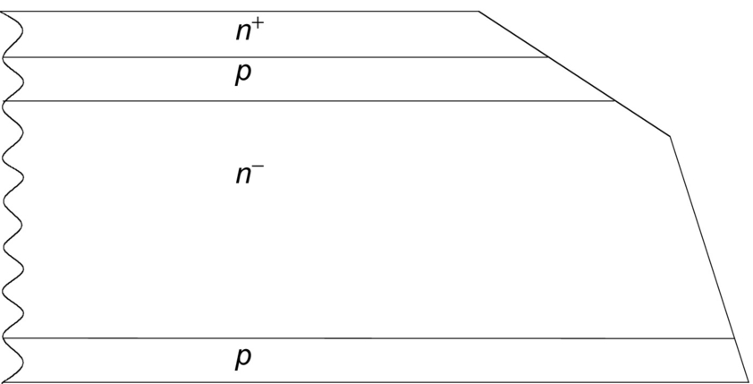
Fig. 3.1 shows a conceptual view of a typical thyristor with the three p-n junctions and the external electrodes labeled. Also shown in the figure is the thyristor circuit symbol used in electric schematics.
A high-resistivity region, n−-base, is present in all thyristors. It is this region, the n−-base and associated junction, J2 of Fig. 3.1, which must support the large applied forward voltages that occur when the switch is in its off- or forward-blocking state (nonconducting). The n−-base is typically doped with impurity phosphorous atoms at a concentration of 1013–1014 cm−3. The n−-base can be tens to hundreds of micrometer thick to support large voltages. High-voltage thyristors are generally made by diffusing aluminum or gallium into both surfaces to create p-doped regions forming deep junctions with the n−-base. The doping profile of the p-regions ranges from about 1015 to 1017 cm−3. These p-regions can be up to tens of micrometer thick. The cathode region (typically only a few micrometers thick) is formed by using phosphorous atoms at a doping density of 1017–1018 cm−3.
The higher the forward-blocking voltage rating of the thyristor, the thicker the n−-base region must be. However, increasing the thickness of this high-resistivity region results in slower turn-on and turn-off (i.e., longer switching times and/or lower frequency of switching cycles because of more stored charge during conduction). For example, a device rated for a forward-blocking voltage of 1 kV will, by its physical construction, switch much more slowly than one rated for 100 V. In addition, the thicker high-resistivity region of the 1 kV device will cause a larger forward voltage drop during conduction than the 100 V device carrying the same current. Impurity atoms, such as platinum or gold, and electron irradiation are used to create charge-carrier recombination sites in the thyristor. The large number of recombination sites reduces the mean carrier lifetime (average time that an electron or hole moves through the Si before recombining with its opposite charge-carrier type). A reduced carrier lifetime shortens the switching times (in particular the turnoff or recovery time) at the expense of increasing the forward conduction drop. There are other effects associated with the relative thickness and layout of the various regions that make up modern thyristors, but the major trade-off between forward-blocking voltage rating and switching times and between forward-blocking voltage rating and forward voltage drop during conduction should be kept in mind. (In signal-level electronics, an analogous trade-off appears as a lowering of amplification (gain) to achieve higher operating frequencies and is often referred to as the gain-bandwidth product.)
Operation of thyristors is as follows. When a positive voltage is applied to the anode (with respect to cathode), the thyristor is in its forward-blocking state. The center junction J2 (see Fig. 3.1) is reverse biased. In this operating mode, the gate current is held to zero (open circuit). In practice, the gate electrode is biased to a small negative voltage (with respect to the cathode) to reverse bias the GK junction J3 and prevent charge carriers from being injected into the p-base. In this condition, only thermally generated leakage current flows through the device and can often be approximated as zero in value (the actual value of the leakage current is typically many orders of magnitude lower than the conducted current in the on-state). As long as the forward applied voltage does not exceed the value necessary to cause excessive carrier multiplication in the depletion region around J2 (avalanche breakdown), the thyristor remains in an off-state (forward-blocking). If the applied voltage exceeds the maximum forward-blocking voltage of the thyristor, it will switch to its on-state. However, this mode of turn-on causes nonuniformity in the current flow, is generally destructive, and should be avoided.
When a positive gate current is injected into the device, J3 becomes forward biased and electrons are injected from the n-emitter into the p-base. Some of these electrons diffuse across the p-base and get collected in the n−-base. This collected charge causes a change in the bias condition of J1. The change in bias of J1 causes holes to be injected from the p-emitter into the n−-base. These holes diffuse across the n−-base and are collected in the p-base. The addition of these collected holes in the p-base acts the same as gate current. The entire process is regenerative and will cause the increase in charge carriers until J2 also becomes forward biased and the thyristor is latched in its on-state (forward conduction). The regenerative action will take place as long as the gate current is applied in sufficient amount and for a sufficient length of time. This mode of turn-on is considered to be the desired one as it is controlled by the gate signal.
This switching behavior can also be explained in terms of the two-transistor analog shown in Fig. 3.2. The two transistors are regeneratively coupled so that if the sum of their forward current gains (α's) exceeds unity, each drives the other into saturation. Eq. (3.1) describes the condition necessary for the thyristor to move from a forward-blocking state to the forward-conduction state. The forward current gain (expressed as the ratio of collector current to emitter current) of the pnp transistor is denoted by αp and that of the npn as αn. The α's are current dependent and increase slightly as the current increases. The center junction J2 is reverse biased under forward applied voltage (positive, vAK). The associated electric field in the depletion region around the junction can result in significant carrier multiplication, denoted as a multiplying factor M on the current components, Ico and iG.

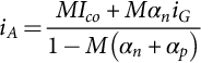
In the forward-blocking state, the leakage current Ico is small, both α's are small, and their sum is less than unity. Gate current increases the current in both transistors, increasing their α's. Collector current in the npn transistor acts as base current for the pnp, and analogously, the collector current of the pnp acts as base current driving the npn transistor. When the sum of the two α's equals unity, the thyristor switches to its on-state (latches). This condition can also be reached, without any gate current, by increasing the forward applied voltage so that carrier multiplication (M≫1) at J2 increases the internal leakage current, thus increasing the two α's. A third way to increase the α's exists by increasing the device (junction) temperature. Increasing the temperature causes a corresponding increase in the leakage current Ico to the point where latching can occur. The typical manifestation of this temperature dependence is to cause an effective lowering of the maximum blocking voltage that can be sustained by the thyristor.
Another way to cause a thyristor to switch from forward-blocking to forward-conduction exists. Under a forward applied voltage, J2 is reverse biased, while the other two junctions are forward biased in the blocking mode. The reverse-biased junction of J2 is the dominant capacitance of the three and determines the displacement current that flows. If the rate of increase in the applied vAK(dvAK/dt) is sufficient, it will cause a significant displacement current through the J2 capacitance. This displacement current can initiate switching similar to an externally applied gate current. This dynamic phenomenon is inherent in all thyristors and causes there to be a limit (dv/dt) to the time rate of applied vAK that can be placed on the device to avoid uncontrolled switching. Alterations to the basic thyristor structure can be produced that increase the dv/dt limit.
Once the thyristor has moved into forward conduction, any applied gate current is superfluous. The thyristor is latched and, for SCRs, cannot be returned to a blocking mode by using the gate terminal. Anode current must be commutated away from the SCR for a sufficient time to allow stored charge in the device to recombine. Only after this recovery time has occurred, can a forward voltage be reapplied (below the dv/dt limit of course), and the SCR again be operated in a forward-blocking mode. If the forward voltage is reapplied before sufficient recovery time has elapsed, the SCR will move back into forward conduction. For GTOs and IGCTs, a large applied reverse gate current (typically in the range of 10%–50% of the anode current for GTOs and 100% of the anode current for IGCTs) applied for a sufficient time can remove enough charge near the GK junction to cause it to turn off. This interrupts the base current to the pnp transistor, leaving the pnp open base, causing thyristor turn-off. This is similar in principle to use negative base current to quickly turn off a traditional bipolar transistor.
3.3 Static Characteristics
3.3.1 Current–Voltage Curves for Thyristors
A plot of the anode current (iA) as a function of anode-cathode voltage (vAK) is shown in Fig. 3.3. The forward-blocking mode is shown as the low-current portion of the graph (solid curve around operating point “1”). With zero gate current and positive vAK, the forward characteristic in the off- or blocking state is determined by the center junction J2, which is reverse biased. At operating point “1,” very little current flows (Ico only) through the device. However, if the applied voltage exceeds the forward-blocking voltage, the thyristor switches to its on- or conducting state (shown as operating point “2”) because of carrier multiplication (M in Eq. (3.1)). The effect of gate current is to lower the blocking voltage at which switching takes place. The thyristor moves rapidly along the negatively sloped portion of the curve until it reaches a stable operating point determined by the external circuit (point “2”). The portion of the graph indicating forward conduction shows the large values of iA that may be conducted at relatively low values of vAK, similar to a power diode.

As the thyristor moves from forward-blocking to forward-conducting, the external circuit must allow sufficient anode current to flow to keep the device latched. The minimum anode current that will cause the device to remain in forward conduction as it switches from forward-blocking is called the latching current IL. If the thyristor is already in forward conduction and the anode current is reduced, the device can move its operating mode from forward conduction back to forward-blocking. The minimum value of anode current necessary to keep the device in forward conduction after it has been operating at a high anode current value is called the holding current IH. The holding current value is lower than the latching current value as indicated in Fig. 3.3.
The reverse thyristor characteristic, quadrant III of Fig. 3.3, is determined by the outer two junctions (J1 and J3), which are reverse biased in this operating mode (applied vAK is negative). Symmetrical thyristors are designed so that J1 will reach reverse breakdown due to carrier multiplication at an applied reverse potential near the forward breakdown value (operating point “3” in Fig. 3.3). The forward- and reverse-blocking junctions are usually fabricated at the same time with a very long diffusion process (10–50 h) at high temperatures (>1200°C). This process produces symmetrical blocking properties. Wafer-edge termination processing causes the forward-blocking capability to be reduced to about 90% of the reverse-blocking capability. Edge termination is discussed below. Asymmetrical devices are made to optimize forward conduction and turnoff properties and as such reach reverse breakdown at a lower voltage than that applied in the forward direction. This is accomplished by designing the asymmetrical thyristor with a much thinner n−-base than is used in symmetrical structures. The thin n−-base leads to improved properties such as lower forward drop and shorter switching times. Asymmetrical devices are generally used in applications when only forward voltages (positive, vAK) are to be applied (including many inverter designs).
The form of the gate-to-cathode i-v characteristic of SCRs, GTOs, and IGCTs is similar to that of a diode. With positive gate bias, the gate-cathode junction is forward biased and permits the flow of a large current in the presence of a low voltage drop. When negative gate voltage is applied to an SCR, the gate-cathode junction is reverse biased and prevents the flow of current until the avalanche breakdown voltage is reached. In a GTO or IGCT, a negative gate voltage is applied to provide a low-impedance path for anode current to flow out of the device instead of out the cathode. In this way, the cathode region (base-emitter junction of the equivalent npn transistor) turns off, thus pulling the equivalent npn transistor out of conduction. This causes the entire thyristor to return to its blocking state. The problem with the GTO and IGCT is that the gate-drive circuitry is typically required to sink 10%–50% (for the GTO) or 100% (for the IGCT) of the anode current to achieve turn-off.
3.3.2 Edge and Surface Terminations
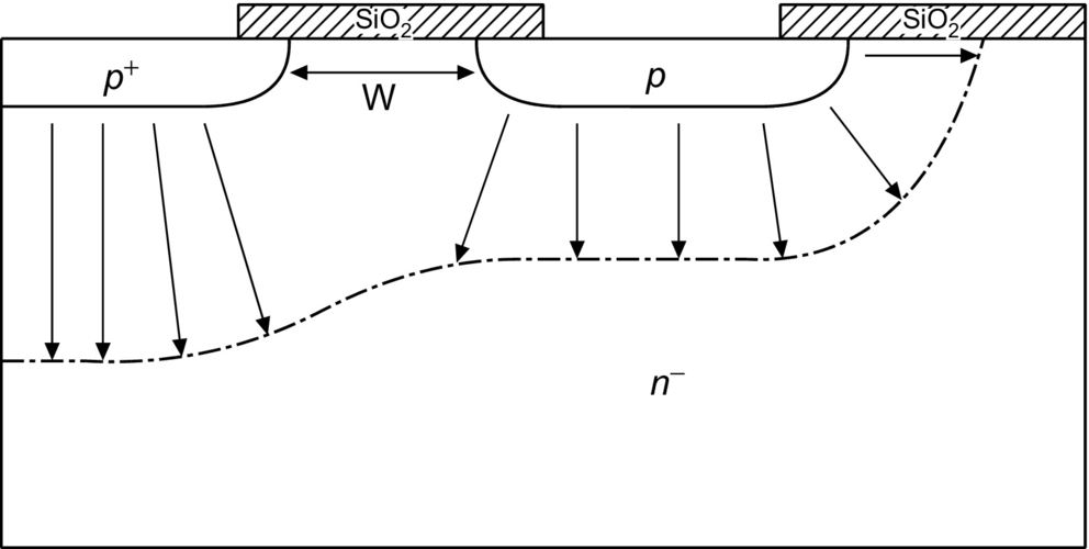
Thyristors are often made with planar diffusion technology to create the cathode region. Formation of these regions creates cylindrical curvature of the metallurgical gate-cathode junction. Under reverse bias, the curvature of the associated depletion region results in electric field crowding along the curved section of the p+ diffused region. The field crowding seriously reduces the breakdown potential below that expected for the bulk semiconductor. A floating field ring, an extra p diffused region with no electric connection at the surface, is often added to modify the electric field profile and thus reduce it to a value below or at the field strength in the bulk. An illustration of a single floating field ring is shown in Fig. 3.4. The spacing, W, between the main anode region and the field ring is critical. Multiple rings can also be employed to further modify the electric field in high-voltage rated thyristors.
Another common method for altering the electric field at the surface is by using a field plate as shown in cross section in Fig. 3.5. By forcing the potential over the oxide to be the same as at the surface of the p+ region, the depletion region can be extended so that the electric field intensity is reduced near the curved portion of the diffused p+ region. A common practice is to use field plates with floating field rings to obtain optimum breakdown performance.

High-voltage thyristors are made from single wafers of Si and must have edge terminations other than floating field rings or field plates to promote bulk breakdown and limit leakage current at the surface. Controlled bevel angles can be created using lapping and polishing techniques during production of large-area thyristors. Two types of bevel junctions can be created: (i) a positive bevel defined as one in which the junction area decreases when moving from the highly doped to the lightly doped side of the depletion region and (ii) a negative bevel defined as one in which the junction area increases when moving from the highly doped to the lightly doped side of the depletion region. In practice, the negative bevel must be lapped at an extremely shallow angle to reduce the surface field below the field intensity in the bulk. All positive bevel angles between 0 and 90 degrees result in a lower surface field than in the bulk. Fig. 3.6 shows the use of a positive bevel for the J1 junction and a shallow negative bevel for the J2 and J3 junctions on a thyristor cross section to make maximum use of the Si area for conduction and still reduce the surface electric field. Further details of the use of beveling, field plates, and field rings can be found in Ghandi [1] and Baliga [2].
3.3.3 Packaging
Thyristors are available in a wide variety of packages, from small plastic ones for low-power (i.e., TO-247), to stud-mount packages for medium-power, to press pack (also called flat pack) for the highest power devices. The press packs must be mounted under pressure to obtain proper electric and thermal contact between the device and the external metal electrodes. Special force-calibrated clamps are made for this purpose. Large-area thyristors cannot be directly attached to the large copper pole piece of the press pack because of the difference in the coefficient of thermal expansion (CTE), hence the use of a pressure contact for both anode and cathode. Fig. 3.7 shows typical thyristor stud-mount and press-pack packages.

Many medium-power thyristors are appearing in modules where a half- or full bridge (and associated antiparallel diodes) is put together in one package. A power module package should have five characteristics:
(i) Electric isolation of the baseplate from the semiconductor
(ii) Good thermal performance
(iii) Good electric performance
(iv) Long life/high reliability
(v) Low cost
Electric isolation of the baseplate from the semiconductor is necessary in order to contain both halves of a phase leg in one package and for convenience (modules switching different phases can be mounted on one heat sink) and safety (heat sinks can be held at ground potential).
Thermal performance is measured by the maximum temperature rise in the Si die at a given power dissipation level with a fixed heat sink temperature. The lower the die temperature, the better the package. A package with a low thermal resistance from junction-to-sink can operate at higher power densities for the same temperature rise or lower temperatures for the same power dissipation than a more thermally resistive package. While maintaining low device temperature is generally preferable, temperature variation affects majority carrier and bipolar devices differently. Roughly speaking, in a bipolar device such as a thyristor, switching losses increase and conduction losses decrease with increasing temperature. In a majority carrier device, such as a MOSFET, conduction losses increase with increasing temperature. The thermal conductivity of typical materials used in thyristor packages is shown in Table 3.1.
Table 3.1
Thermal conductivity of thyristor package materials
| Material | Thermal conductivity (W/m·K) at 300 K |
| Silicon | 150 |
| Copper (baseplate and pole pieces) | 390–400 |
| AlN substrate | 170 |
| Al2O3 (alumina) | 28 |
| Aluminum (Al) | 220 |
| Tungsten (W) | 167 |
| Molybdenum (Mo) | 138 |
| Metal matrix composites (MMC) | 170 |
| Thermal grease (heat sink compound) | 0.75 |
| 60/40 solder (Pb/Sn eutectic) | 50 |
| 95/5 solder (Pb/Sn high temperature) | 35 |
Electric performance refers primarily to the stray inductance in series with the die and the capability of mounting a low-inductance bus to the terminals. Another problem is the minimization of capacitive cross talk from one switch to another, which can cause an abnormal on-state condition by charging the gate of an off-state switch or from a switch to any circuitry in the package (as would be found in a hybrid power module). Capacitive coupling is a major cause of electromagnetic interference (EMI). As the stray inductance of the module and the bus sets a minimum switching loss for the device—because the switch must absorb the stored inductive energy—it is very important to minimize inductance within the module. Reducing the parasitic inductance reduces the high-frequency ringing during transients that is another cause of radiated EMI. Since stray inductance can cause large peak voltages during switching transients, minimizing it helps to maintain the device within its safe area of operation.
Long life and high reliability are primarily attained through minimization of thermal cycling, minimization of ambient temperature, and proper design of the transistor stack. Thermal cycling fatigues material interfaces because of CTE mismatch between dissimilar materials. As the materials undergo temperature variation, they expand and contract at different rates that stresses the interface between the layers and can cause interface deterioration (e.g., cracking of solder layers or wire debonding). Chemical degradation processes such as dendrite growth and impurity migration are accelerated with increasing temperature, so keeping the absolute temperature of the device low and minimizing the temperature changes to which it is subjected is important. Typical CTE values for common package materials are given in Table 3.2.
Table 3.2
CTE for thyristor package materials
| Material | CTE (μm/m·K) at 300 K |
| Silicon | 4.1 |
| Copper (baseplate and pole pieces) | 17 |
| AlN substrate | 4.5 |
| Al2O3 (Alumina) | 6.5 |
| Tungsten (W) | 4.6 |
| Molybdenum (Mo) | 4.9 |
| Aluminum (Al) | 23 |
| Metal matrix composites (MMC) | 5–20 |
| 60/40 solder (Pb/Sn eutectic) | 25 |
Low cost is achieved in a variety of ways. Both manufacturing and material costs must be taken into account when designing a power module. Materials that are difficult to machine or process, even if they are relatively cheap in raw form (e.g., molybdenum), should be avoided. Manufacturing processes that lower yield also drive up costs. In addition, a part that is very reliable can reduce future costs by reducing the need for repair and replacement.
The basic half-bridge module has three power terminals: plus, minus, and phase. Advanced modules differ from traditional high-power commercial modules in several ways. The baseplate is metallized aluminum nitride (AlN) ceramic rather than the typical 0.125 in. thick nickel-plated copper baseplate with a soldered metallized ceramic substrate for electric isolation. This AlN baseplate stack provides a low thermal resistance from die to heat sink. The copper terminal power buses are attached by solder to the devices in a wirebond-free, low-inductance, low-resistance, device interconnect configuration. The balance of the assembly is typical for module manufacturing with attachment of shells, use of dielectric gels, and hard epoxies and adhesive to seal the finished module. Details of the thermal performance of modules and advanced modules can be found in Beker et al. [3] and Godbold et al. [4].
3.4 Dynamic Switching Characteristics
The time rate of rise of anode current (di/dt) during turn-on and the time rate of rise of anode-cathode voltage (dv/dt) during turnoff are important parameters to control for ensuring proper and reliable operation. All thyristors have maximum limits for di/dt and dv/dt that must not be exceeded. Devices capable of conducting large currents in the on-state are necessarily made with large surface areas through which the current flows. During turn-on, localized areas of a device (near the gate region) begin to conduct current. The initial turn-on of an SCR is shown in Fig. 3.8. The cross section illustrates how injected gate current flows to the nearest cathode region, causing this portion of the npn transistor to begin conducting. The pnp transistor then follows the npn into conduction such that anode current begins flowing only in a small portion of the cathode region. If the local current density becomes too large (in excess of several thousand amperes per square centimeter), then self-heating will damage the device. Sufficient time (referred to as plasma spreading time) must be allowed for the entire cathode area to begin conducting before the localized currents become too high. This phenomenon results in a maximum allowable rate of rise of anode current in a thyristor and is referred to as a di/dt limit. In many high-frequency applications, the entire cathode region is never fully in conduction. Prevention of di/dt failure can be accomplished if the rate of increase of conduction area exceeds the di/dt rate such that the internal junction temperature does not exceed a specified critical temperature (typically approximately 350°C). This critical temperature decreases as the blocking voltage increases. Adding series inductance to the thyristor to limit di/dt below its maximum usually causes circuit design problems.

Another way to increase the di/dt rating of a device is to increase the amount of gate-cathode periphery. Inverter SCRs (so-named because of their use in high-frequency power-converter circuits that convert dc to ac, i.e., invert) are designed so that there is a large amount of gate edge adjacent to a significant amount of cathode edge. A top surface view of two typical gate-cathode patterns, found in large thyristors, is shown in Fig. 3.9. An inverter SCR often has a stated maximum di/dt limit of approximately 2000 A/μs. This value has been shown to be conservative in Hadgins [5], and by using excessive gate current under certain operating conditions, an inverter SCR can be operated reliably at 10,000–20,000 A/μs.
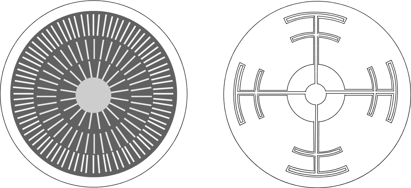
A GTO takes the interdigitation of the gate and cathode to the extreme (Fig. 3.9, left). In Fig. 3.10, a cross section of a GTO shows the amount of interdigitation. A GTO often has cathode islands that are formed by etching the Si. A metal plate can be placed on the top to connect the individual cathodes into a large arrangement of electrically parallel cathodes. The gate metallization is placed so that the gate surrounding each cathode is electrically in parallel as well. This construction not only allows high di/dt values to be reached, as in an inverter SCR but also provides the capability to turn off the anode current by shunting it away from the individual cathodes and out of the gate electrode upon reverse biasing of the gate. During turnoff, current is decreasing while voltage across the device is increasing. If the forward voltage becomes too high while sufficient current is still flowing, then the device will drop back into its conduction mode instead of completing its turn-off cycle. Also, during turnoff, the power dissipation can become excessive if the current and voltage are simultaneously too large. Both of these turn-off problems can damage the device and other portions of the circuit.

Another switching problem that occurs is associated primarily with thyristors, though other power electronic devices suffer some degradation of performance from the same problem. This problem is that thyristors can self-trigger into a forward-conduction mode from a forward-blocking mode if the rate of rise of forward anode-cathode voltage is too large. This triggering method is due to displacement current through the associated junction capacitances (the capacitance at J2 dominates because it is reverse biased under forward applied voltage). The displacement current contributes to the leakage current Ico, shown in Eq. (3.1). The SCRs, GTOs, and IGCTs, therefore, have a maximum dv/dt rating that should not be exceeded (typical values are 100–1000 V/μs). Switching into a reverse-conducting from a reverse-blocking state, due to an applied reverse dv/dt, is not possible because the values of the reverse α's of the equivalent transistors can never be made large enough to cause the necessary feedback (latching) effect. An external capacitor is often placed between the anode and cathode of the thyristor to help control the dv/dt experienced. Capacitors and other components that are used to form such protection circuits, known as snubbers, may be found in all power semiconductor devices.
3.4.1 Cathode Shorts
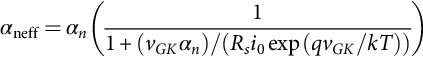
As the temperature in the thyristor increases above 25°C, the minority carrier lifetime and the corresponding diffusion lengths in the n- and p-bases increase. This leads to an increase in the α's of the equivalent transistors. Discussion of the details of the minority carrier diffusion length and its role in determining the current gain factor α can be found in Sze [6]. Referring to Eq. (3.1), it is seen that a lower applied bias will give a carrier multiplication factor M sufficient to switch the device from forward-blocking into conduction, because of this increase of the α's with increasing temperature. Placing a shunt resistor in parallel with the base-emitter junction of the equivalent npn transistor (shown in Fig. 3.11) will result in an effective current gain, αneff, that is lower than αn, as given by Eq. (3.2), where vGK is the applied gate-cathode voltage, Rs is the equivalent lumped value for the distributed current shunting structure, and the remaining factors form the appropriate current factor based on the applied bias and characteristics of the gate-cathode junction. The shunt current path is implemented by providing intermittent shorts, called cathode shorts, between the p-base (gate) region and the n+-emitter (cathode) region in the thyristor as illustrated in Fig. 3.12. The lumped shunt resistance value is in the range of 1–15 Ω as measured from gate to cathode.

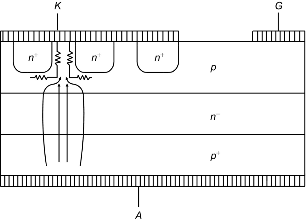
Low values of anode current (e.g., those associated with an increase in temperature under forward-blocking conditions) will flow through the shunt path to the cathode contact, bypassing the n+-emitter and keeping the device out of its forward-conduction mode. As the anode current becomes large, the potential drop across the shunt resistance will be sufficient to forward bias the gate-cathode junction, J3, and bring the thyristor into forward conduction. The cathode shorts also provide a path for displacement current to flow without forward-biasing J3. The dv/dt rating of the thyristor is thus improved and the forward-blocking characteristics by using cathode shorts. However, the shorts do cause a lowering of cathode current handling capability because of the loss of some of the cathode area (n+-region) to the shorting pattern, an increase in the necessary gate current to obtain switching from forward-blocking to forward conduction and an increase in complexity of manufacturing of the thyristor. The loss of cathode area due to the shorting structure is from 5% to 20%, depending on the type of thyristor. By careful design of the cathode short windows to the p-base, the holding current can be made lower than the latching current. This is important so that the thyristor will remain in forward conduction when used with varying load impedances.
3.4.2 Anode Shorts
A further increase in forward-blocking capability can be obtained by introducing anode shorts in addition to the cathode shorts. This reduces αp in a similar manner that cathode shorts reduce αn. An illustration of this is provided in Fig. 3.13. In this structure, both J1 and J3 are shorted (anode and cathode shorts), so that the forward-blocking capability of the thyristor is completely determined by the avalanche breakdown characteristics of J2. Anode shorts will result in the complete loss of reverse-blocking capability and are only suitable for thyristors used in asymmetrical circuit applications.

3.4.3 Amplifying Gate
The cathode-shorting structure will reduce the gate sensitivity dramatically. To increase this sensitivity and yet retain the benefits of the cathode shorts, a structure called an amplifying gate (or regenerative gate) is used, as shown in Fig. 3.14 (and Fig. 3.9, right). When the gate current (1) is injected into the p-base through the pilot-gate contact, electrons are injected into the p-base by the n+-emitter with a given emitter injection efficiency. These electrons traverse through the p-base (the time taken for this process is called the transit time) and accumulate near the depletion region. This negative charge accumulation leads to injection of holes from the anode. The device then turns on after a certain delay, dictated by the p-base transit time, and the pilot anode current (2) begins to flow through a small region near the pilot-gate contact as shown in Fig. 3.14.

This flow of pilot anode current corresponds to the initial sharp rise in the anode current waveform (phase I), as shown in Fig. 3.15. The device switching then goes into phase II, during which the anode current remains fairly constant, suggesting that the resistance of the region has reached its lower limit. This is due to the fact that the pilot anode current (2) takes a finite time to traverse through the p-base laterally and become the gate current for the main cathode area. The n+-emitters start to inject electrons which traverse the p-base vertically and after a certain finite time (transit time of the p-base) reach the depletion region. The total time taken by the lateral traversal of pilot anode current and the electron transit time across the p-base is the reason for observing this characteristic phase II interval. The width of the phase II interval is comparable to the switching delay, suggesting that the p-base transit time is of primary importance. Once the main cathode region turns on, the resistance of the device decreases and the anode current begins to rise again (transition from phase II to III). From this time onward in the switching cycle, the plasma spreading velocity will dictate the rate at which the conduction area will increase. The current density during phases I and II can be quite large, leading to a considerable increase in the local temperature and device failure. The detailed effect of the amplifying gate on the anode current rise will only be noticed at high levels of di/dt (in the range of 1000 A/μs), shown in Fig. 3.15. It can be concluded that the amplifying gate will increase gate sensitivity at the expense of some di/dt capability, as demonstrated by Sankaran [7]. This lowering of di/dt capability can be somewhat offset by an increase in gate-cathode interdigitation as previously discussed.

3.4.4 Temperature Dependencies
The forward-blocking voltage of an SCR has been shown to be reduced from 1350 V at 25°C to 950 V at −175°C in a near linear fashion [8]. Above 25°C, the forward-blocking capability is again reduced, due to changes in the minority carrier lifetime, which cause the leakage current to increase and the associated breakover voltage to decrease. Several dominant physical parameters associated with semiconductor devices are sensitive to temperature variations, causing their dependent device characteristics to change dramatically. The most important of these parameters are (i) the minority carrier lifetimes (which control the high-level injection lifetimes), (ii) the hole and electron mobilities, (iii) the impact ionization collision cross sections, and (iv) the free-carrier concentrations (primarily the ionized impurity atom concentration). Almost all of the impurity atoms are ionized at temperatures above 0°C, and so further discussion of the temperature effects on ionization is not relevant for normal operation. As the temperature increases above 25°C, the following trends are observed: the carrier lifetimes increase, giving longer recovery times and greater switching losses; the carrier mobilities are reduced, increasing the on-state voltage drop; and at very high temperatures, the intrinsic carrier concentration becomes sufficiently high that the depletion layer will not form and the device cannot switch off. A more detailed discussion of these physical parameters is beyond the scope of this book, but references are listed for those persons interested in pursuing relevant information about temperature effects.
It is well known that charge-carrier recombination events are more efficient at lower temperatures. This shows up as a larger potential drop during forward conduction and a shorter recovery time during turnoff. A plot of the anode current during turnoff, at various temperatures, for a typical GTO is shown in Fig. 3.16.

An approximate relation between the temperature and the forward drop across the n−-base of a thyristor is discussed in detail by Herlet [9] and Hudgins et al. [10]. Temperature-dependent equations relating the anode current density, JA, and the applied anode-cathode voltage VAK are also given in Ref. [10]; these include the junction potential drops in the device, the temperature dependence of the band-gap energy, and the n−-base potential drop. Data from measurements at forward current densities of approximately 100 A/cm2 on a GTO rated for 1 kV symmetrical blocking give forward voltage drops of 1.7 V at −50°C and 1.8 V at 150°C.
3.5 Thyristor Parameters
Understanding of a thyristor's maximum ratings and electric characteristics is required for proper application. Use of a manufacturer's data sheet is essential for good design practice. Ratings are maximum or minimum values that set limits on device capability. A measure of device performance under specified operating conditions is a characteristic of the device. A summary of some of the maximum ratings that must be considered when choosing a thyristor for a given application is provided in Table 3.3. Thyristor types shown in parentheses indicate a maximum rating unique to that device. Both forward and reverse repetitive and nonrepetitive voltage ratings must be considered, and a properly rated device must be chosen so that the maximum voltage ratings are never exceeded. In most cases, either forward- or reverse-voltage transients in excess of the nonrepetitive maximum ratings result in destruction of the device. The maximum root mean square (RMS) or average current ratings given are usually those which cause the junction to reach its maximum rated temperature. Because the maximum current will depend upon the current waveform and upon thermal conditions external to the device, the rating is usually shown as a function of case temperature and conduction angle. The peak single half-cycle surge-current rating must be considered, and in applications where the thyristor must be protected from damage by overloads, a fuse with an I2t rating smaller than the maximum rated value for the device must be used. Maximum ratings for both forward and reverse gate voltage, current, and power also must not be exceeded.
Table 3.3
Thyristor maximum ratings specified by manufacturers
| Symbol | Description |
| VRRM | Peak repetitive reverse voltage |
| VRSM | Peak nonrepetitive reverse voltage (transient) |
| VR(DC) | DC reverse-blocking voltage |
| VDRM | Peak repetitive forward off-state voltage |
| VDSM | Peak nonrepetitive forward off-state voltage (transient) |
| VD(DC) | DC forward-blocking voltage |
| IT(RMS),IF(RMS) | RMS forward on-state current |
| IT(AV),IF(AV) | Average forward on-state current at specified case or junction temperature |
| ITSM,IF(TSM) | Peak one-cycle surge on-state current (values specified at 60 and 50 Hz) |
| ITGQ (GTO) | Peak controllable current |
| I2t | Nonrepetitive pulse overcurrent capability (t=8.3 ms for a 60 Hz half cycle) |
| PT | Maximum power dissipation |
| di/dt | Critical rate of rise of on-state current at specified junction temperature, gate current, and forward-blocking voltage |
| PGM (PFGM for GTO) | Peak gate power dissipation (forward) |
| PRGM (GTO) | Peak gate power dissipation (reverse) |
| PG(AV) | Average gate power dissipation |
| VFGM | Peak forward gate voltage |
| VRGM | Peak reverse gate voltage |
| IFGM | Peak forward gate current |
| IRGM (GTO) | Peak reverse gate current |
| TSTG | Storage temperature |
| Tj | Junction operating temperature |
| VRMS | Voltage isolation (modules) |
The maximum rated operating junction temperature TJ must not be exceeded, since device performance, in particular voltage-blocking capability, will be degraded. Junction temperature cannot be measured directly but must be calculated from a knowledge of steady-state thermal resistance ![]() and the average power dissipation. For transients or surges, the transient thermal impedance (
and the average power dissipation. For transients or surges, the transient thermal impedance (![]() ) curve must be used (provided in manufacturer's data sheets). The maximum average power dissipation PT is related to the maximum rated operating junction temperature and the case temperature by the steady-state thermal resistance. In general, both the maximum dissipation and its derating with increasing case temperature are provided.
) curve must be used (provided in manufacturer's data sheets). The maximum average power dissipation PT is related to the maximum rated operating junction temperature and the case temperature by the steady-state thermal resistance. In general, both the maximum dissipation and its derating with increasing case temperature are provided.
The number and type of thyristor characteristics specified varies widely from one manufacturer to another. Some characteristics are given only as typical values of minima or maxima, while many characteristics are displayed graphically. Table 3.4 summarizes some of the typical characteristics provided as maximum values. The maximum value means that the manufacturer guarantees that the device will not exceed the value given under the specified operating or switching conditions. A minimum value means that the manufacturer guarantees that the device will perform at least, as well as the characteristic given under the specified operating or switching conditions. Thyristor types shown in parenthesis indicate a characteristic unique to that device. Gate conditions of both voltage and current to ensure either nontriggered or triggered device operation are included. The turn-on and turn-off transients of the thyristor are characterized by switching times like the turn-off time listed in Table 3.4. The turn-on transient can be divided into three intervals: (i) gate-delay interval, (ii) turn-on of initial area, and (iii) spreading interval. The gate-delay interval is simply the time between application of a turn-on pulse at the gate and the time the initial cathode area turns on. This delay decreases with increasing gate-drive current and is of the order of a few microseconds. The second interval, the time required for turn-on of the initial area, is quite short, typically less than 1 μs. In general, the initial area turned on is a small percentage of the total useful device area. After the initial area turns on, conduction spreads (spreading interval or plasma spreading time) throughout the device in tens of microseconds for high speed or thyristors. The plasma spreading time may take up to hundreds of microseconds in large-area phase-control devices.
Table 3.4
Typical thyristor characteristic maximum and minimum values specified by manufacturers
| Symbol | Description |
| VTM,VFM | Maximum on-state voltage drop (at specified junction temperature and forward current) |
| IDRM | Maximum forward off-state current (at specified junction temperature and forward voltage) |
| IRRM | Maximum reverse off-state current (at specified junction temperature and reverse voltage) |
| dv/dt | Minimum critical rate of rise of off-state voltage at specified junction temperature and forward-blocking voltage level |
| VGT | Maximum gate trigger voltage (at specified temperature and forward applied voltage) |
| VGD,VGDM | Maximum gate nontrigger voltage (at specified temperature and forward applied voltage) |
| IGT | Maximum gate trigger current (at specified temperature and forward applied voltage) |
| Tgt (GTO) | Maximum turn-on time (under specified switching conditions) |
| Tq | Maximum turn-off time (under specified switching conditions) |
| tD | Maximum turn-on delay time (for specified test) |
| Maximum junction-to-case thermal resistance | |
| Maximum case-to-sink thermal resistance (interface lubricated) |
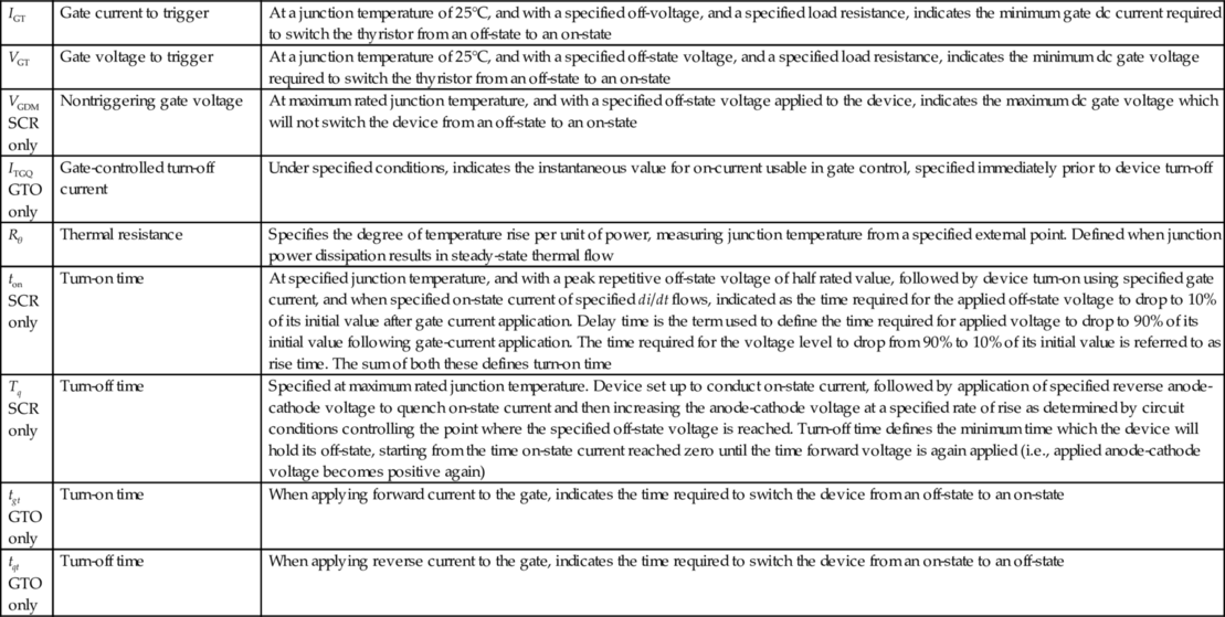
Table 3.5 lists many of the thyristor parameters that appear as listed values or as information on graphs. The definition of each parameter and the test conditions under which they are measured are given in the table as well.
Table 3.5
Symbols and definitions of major thyristor parameters
| Rθ | Thermal Resistance | Specifies the degree of temperature rise per unit of power, measuring junction temperature from a specified external point. Defined when junction power dissipation results in steady-state thermal flow |
| Junction-to-ambient thermal resistance | The steady-state thermal resistance between the junction and ambient | |
| Junction-to-case thermal resistance | The steady-state thermal resistance between the junction and case surface | |
| Junction-to-sink thermal resistance | The steady-state thermal resistance between the junction and the heat sink mounting surface | |
| Contact thermal resistance | The steady-state thermal resistance between the surface of the case and the heat sink mounting surface | |
| Zθ | Transient thermal impedance | The change of temperature difference between two specified points or regions at the end of a time interval divided by the step function change in power dissipation at the beginning of the same interval causing the change of temperature difference |
| Junction-to-ambient transient thermal impedance | The transient thermal impedance between the junction and ambient | |
| Junction-to-case transient thermal impedance | The transient thermal impedance between the junction and the case surface | |
| Junction-to-sink transient thermal impedance | The transient thermal impedance between the junction and the heat sink mounting surface | |
| TA | Ambient temperature | It is the temperature of the surrounding atmosphere of a device when natural or forced-air cooling is used and is not influenced by heat dissipation of the device |
| TS | Sink temperature | The temperature at a specified point on the device heat sink |
| TC | Case temperature | The temperature at a specified point on the device case |
| TJ | Junction temperature | The device junction temperature rating. Specifies the maximum and minimum allowable operation temperatures |
| TSTG | Storage temperature | Specifies the maximum and minimum allowable storage temperatures (with no electric connections) |
| VRRM | Peak reverse-blocking voltage | Within the rated junction temperature range and with the gate terminal open circuited, specifies the repetitive peak reverse anode-to-cathode voltage applicable on each cycle |
| VRSM | Transient peak reverse-blocking voltage | Within the rated junction temperature range and with the gate terminal open circuited, specifies the nonrepetitive peak reverse anode-to-cathode voltage applicable for a time width equivalent to less than 5 ms |
| VR(DC) SCR only | Dc reverse-blocking voltage | Within the rated junction temperature range and with the gate terminal open-circuited, specifies the maximum value for dc anode-to-cathode voltage applicable in the reverse direction |
| VDRM | Peak forward-blocking voltage | Within the rated junction temperature range and with the gate terminal open circuited (SCR) or with a specified reverse voltage between the gate and cathode (GTO), specifies the repetitive peak off-state anode-to-cathode voltage applicable on each cycle. This does not apply for transient off-state voltage application |
| VDSM | Transient peak forward-blocking voltage | Within the rated junction temperature range, and with the gate terminal open circuited (SCR), or with a specified reverse voltage between the gate and cathode (GTO), specifies the nonrepetitive off-state anode-to-cathode voltage applicable for a time width equivalent to less than 5 ms. This gives the maximum instantaneous value for nonrepetitive transient off-state voltage |
| VD(DC) | Dc forward-blocking voltage | Within the rated junction temperature range and with the gate terminal open circuited (SCR) or with a specified reverse voltage between the gate and cathode (GTO), specifies the maximum value for dc anode-to-cathode voltage applicable in the forward direction |
| dv/dt | Critical rate of rise of off-state voltage |
At the maximum rated junction temperature range, and with the gate terminal open circuited (SCR), or with a specified reverse voltage between the gate and cathode (GTO), this specifies the maximum rate of rise of off-state voltage that will not drive the device from an off-state to an on-state when an exponential off-state voltage of specified amplitude is applied to the device |
| VTM | Peak on-state voltage | At specified junction temperature, and when on-state current (50 or 60 Hz, half sine wave of specified peak amplitude) is applied to the device, indicates peak value for the resulting voltage drop |
| IT(RMS) | RMS on-state current | At specified case temperature, indicates the RMS value for on-state current that can be continuously applied to the device |
| IT(AV) | Average on-state current | At specified case temperature, and with the device connected to a resistive or inductive load, indicates the average value for forward current (sine half wave, commercial frequency) that can be continuously applied to the device |
| ITSM | Peak on-state current | Within the rated junction temperature range, indicates the peak value for nonrepetitive on-state current (sine half wave, 50 or 60 Hz). This value indicated for one cycle or as a function of a number of cycles |
| I2t | Current-squared time | The maximum, on-state, nonrepetitive short-time thermal capacity of the device and is helpful in selecting a fuse or providing a coordinated protection scheme of the device in the equipment. This rating is intended specifically for operation less than one half cycle of a 180 (degree) conduction angle sinusoidal wave form. The off-state blocking capability cannot be guaranteed at values near the maximum I2t |
| di/dt | Critical rate of rise of on-state current | At specified case temperature, specified off-state voltage, specified gate conditions, and at a frequency of less than 60 Hz, indicates the maximum rate of rise of on-state current which the thyristor will withstand when switching from an off-state to an on-state, when using recommended gate drive |
| IRRM | Peak reverse leakage current | At maximum rated junction temperature, indicates the peak value for reverse current flow when a voltage (sine half wave, 50 or 60 Hz, and having a peak value as specified for repetitive peak reverse-voltage rating) is applied in a reverse direction to the device |
| IDRM | Peak forward-leakage current | At maximum rated junction temperature, indicates the peak value for off-state current flow when a voltage (sine half wave, 50 or 60 Hz, and having a peak value for repetitive off-state voltage rating) is applied in a forward direction to the device. For a GTO, a reverse voltage between the gate and cathode is specified |
| PGM (SCR) PGFM (GTO) | Peak gate power dissipation peak gate forward power dissipation | Within the rated junction temperature range, indicates the peak value for maximum allowable power dissipation over a specified time period, when the device is in forward conduction between the gate and cathode |
| PG(AV) | Average gate power dissipation | Within the rated junction temperature range, indicates the average value for maximum allowable power dissipation when the device is forward-conducting between the gate and cathode |
| PGRM GTO only | Peak gate reverse power dissipation | Within the rated junction temperature range, indicates the peak value for maximum allowable power dissipation in the reverse direction between the gate and cathode, over a specified time period |
| PGR(AV) GTO only | Average gate reverse power dissipation | Within the rated junction temperature range, indicates the average value for maximum allowable power dissipation in the reverse direction between the gate and cathode |
| IGFM | Peak forward gate current | Within the rated junction temperature range, indicates the peak value for forward current flow between the gate and cathode |
| IGRM GTO only | Peak reverse gate current | Within the rated junction temperature range, indicates peak value for reverse current that can be conducted between the gate and cathode |
| VGRM | Peak reverse gate voltage | Within the rated junction temperature range, indicates the peak value for reverse voltage applied between the gate and cathode |
| VGFM | Peak forward gate voltage | Within the rated junction temperature range, indicates the peak value for forward voltage applied between the gate and cathode |
| IGT | Gate current to trigger | At a junction temperature of 25°C, and with a specified off-voltage, and a specified load resistance, indicates the minimum gate dc current required to switch the thyristor from an off-state to an on-state |
| VGT | Gate voltage to trigger | At a junction temperature of 25°C, and with a specified off-state voltage, and a specified load resistance, indicates the minimum dc gate voltage required to switch the thyristor from an off-state to an on-state |
| VGDM SCR only | Nontriggering gate voltage | At maximum rated junction temperature, and with a specified off-state voltage applied to the device, indicates the maximum dc gate voltage which will not switch the device from an off-state to an on-state |
| ITGQ GTO only | Gate-controlled turn-off current | Under specified conditions, indicates the instantaneous value for on-current usable in gate control, specified immediately prior to device turn-off |
| Rθ | Thermal resistance | Specifies the degree of temperature rise per unit of power, measuring junction temperature from a specified external point. Defined when junction power dissipation results in steady-state thermal flow |
| ton SCR only | Turn-on time | At specified junction temperature, and with a peak repetitive off-state voltage of half rated value, followed by device turn-on using specified gate current, and when specified on-state current of specified di/dt flows, indicated as the time required for the applied off-state voltage to drop to 10% of its initial value after gate current application. Delay time is the term used to define the time required for applied voltage to drop to 90% of its initial value following gate-current application. The time required for the voltage level to drop from 90% to 10% of its initial value is referred to as rise time. The sum of both these defines turn-on time |
| Tq SCR only | Turn-off time | Specified at maximum rated junction temperature. Device set up to conduct on-state current, followed by application of specified reverse anode-cathode voltage to quench on-state current and then increasing the anode-cathode voltage at a specified rate of rise as determined by circuit conditions controlling the point where the specified off-state voltage is reached. Turn-off time defines the minimum time which the device will hold its off-state, starting from the time on-state current reached zero until the time forward voltage is again applied (i.e., applied anode-cathode voltage becomes positive again) |
| tgt GTO only | Turn-on time | When applying forward current to the gate, indicates the time required to switch the device from an off-state to an on-state |
| tqt GTO only | Turn-off time | When applying reverse current to the gate, indicates the time required to switch the device from an on-state to an off-state |

3.6 Types of Thyristors
In recent years, most development effort has gone into continued integration of the gating and control electronics into thyristor modules and the use of MOS technology to create gate structures integrated into the thyristor itself. Many variations of this theme are being developed and some technologies should rise above the others in the years to come. Further details concerning most of the following discussion of thyristor types can be found in [11].
3.6.1 SCRs and GTOs
The highest power handling devices continue to be bipolar thyristors. High-powered thyristors are large diameter devices, some well in excess of 100 mm, and as such have a limitation on the rate of rise of anode current, a di/dt rating. The depletion capacitances around the p-n junctions, in particular the center junction J2, limit the rate of rise in forward voltage that can be applied even after all the stored charge, introduced during conduction, is removed. The associated displacement current under application of forward voltage during the thyristor blocking state sets a dv/dt limit. Some effort in improving the voltage hold-off capability and overvoltage protection of conventional SCRs is underway by incorporating a lateral high-resistivity region to help dissipate the energy during breakover. Most effort, though, is being placed in the further development of high-performance GTOs and IGCTs because of their controllability and to a lesser extent in optically triggered structures that feature gate circuit isolation.
High-voltage GTOs with symmetrical blocking capability require thick n−-base regions to support the high electric field. The addition of an n+ buffer layer next to the p+-anode allows high-voltage forward-blocking and a low forward voltage drop during conduction because of the thinner n−-base required. Cylindrical anode shorts have been incorporated to facilitate excess carrier removal from the n−-base during turnoff and still retain the high blocking capability. This device structure can control 200 A, operating at 900 Hz, with a 6 kV hold-off. Some of the design trade-off between the n−-base width and turn-off energy losses in these structures has been determined. A similar GTO incorporating an n+-buffer layer and a pin structure has been fabricated that can control up to 1 kA (at a forward drop of 4 V) with a forward-blocking capability of 8 kV. A reverse conducting GTO has been fabricated that can block 6 kV in the forward direction, interrupt a peak current of 3 kA, and has a turn-off gain of about 5.
The IGCT is a modified GTO structure. It is designed and manufactured so that it commutates all of the cathode current away from the cathode region and diverts it out of the gate contact. The IGCT is similar to a GTO in structure except that it always has a low-loss n-buffer region between the n−-base and p-emitter. The IGCT device package is designed to result in a very low parasitic inductance and is integrated with a specially designed gate-drive circuit. The gate drive contains all the necessary di/dt and dv/dt protection; the only connections required are a low-voltage power supply for the gate drive and an optical signal for controlling the gate. The specially designed gate drive and ring-gate package circuit allows the IGCT to be operated without a snubber circuit and to switch with a higher anode di/dt than a similar GTO. At blocking voltages of 4.5 kV and higher, the IGCT provides better performance than a conventional GTO. The speed at which the cathode current is diverted to the gate (diGQ/dt) is directly related to the peak snubberless turn-off capability of the IGCT. The gate-drive circuit can sink current for turn-off at diGQ/dt values in excess of 7000 A/μs. This hard gate drive results in a low charge storage time of about 1 μs. The low storage time and the fail-short mode make the IGCT attractive for high-power, high-voltage series applications; examples include high-power converters in excess of 100 MVA, static volt-ampere reactive (VAR) compensators, and converters for distributed generation such as wind power.
3.6.1.1 On-State Characteristics
In the on-state, the GTO operates in a similar manner to the thyristor. If the anode current remains above the holding current level, then positive gate drive may be reduced to zero, and the GTO will remain in conduction. However, as a result of the turn-off ability of the GTO, it does possess a higher holding current level than the standard thyristor, and in addition, the cathode of the GTO thyristor is subdivided into small finger elements to assist turn-off. Thus, if the GTO thyristor anode current transiently dips below the holding current level, localized regions of the device may turn off, thus forcing a high anode current back into the GTO at a high rate of rise of anode current after this partial turnoff. This situation could be potentially destructive. It is recommended, therefore, that the positive gate drive is not removed during conduction but is held at a value IG(ON), where IG(ON) is greater than the maximum critical trigger current (IGT) over the expected operating temperature range of the GTO thyristor.
Fig. 3.17 shows the typical on-state V-I characteristics for a 40001A, 4500 V GTO from Dynex range of GTOs [1] at junction temperatures of 25 and 125°C. The curves can be approximated to a straight line of the form

where V0=voltage intercept models the voltage across the cathode and anode forward-biased junctions and R0=on-state resistance. When average and RMS values of on-state current (ITAV, ITRMS) are known, then the on-state power dissipation PON can be determined using V0 and R0. That is,
3.6.1.2 Off-State Characteristics
Unlike the standard thyristor, the GTO does not include cathode emitter shorts to prevent nongated turn-on effects due to dv/dt induced forward-biased leakage current. In the off-state of the GTO, steps should, therefore, be taken to prevent such potentially dangerous triggering. This can be accomplished by either connecting the recommended value of resistance between the gate and the cathode (RGK) or by maintaining a small reverse bias on the gate contact (VRG=−2 V). This will prevent the cathode emitter becoming forward biased and therefore sustain the GTO thyristor in the off-state.
The peak off-state voltage is a function of resistance RGK. This is shown in Fig. 3.18. Under ordinary operating conditions, GTOs are biased with a negative gate voltage of around −15 V supplied from the gate-drive unit during the off-state interval. Nevertheless, provision of RGK may be desirable design practice in the event of the gate-drive failure for any reason (![]() is recommended for a large GTO). RGK dissipates energy and hence adds to the system losses.
is recommended for a large GTO). RGK dissipates energy and hence adds to the system losses.

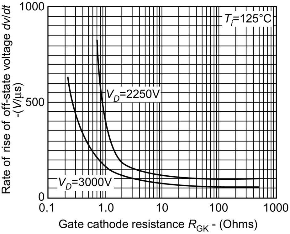
3.6.1.3 Rate of Rise of Off-State Voltage (dvD/dt)
The rate of rise of off-state voltage (dvD/dt) depends on the resistance RGK connected between the gate and the cathode and the reverse bias applied between the gate and the cathode. This relationship is shown in Fig. 3.19.
3.6.1.4 Gate Triggering Characteristics
The gate trigger current (IGT) and the gate trigger voltage (VGT) are both dependent on junction temperature Tj as shown in Fig. 3.20. During the conduction state of the GTO, a certain value of gate current must be supplied, and this value should be larger than the IGT at the lowest junction temperature at which the GTO operates. In dynamic conditions, the specified IGT is not sufficient to trigger the GTO switching from higher voltage and high di/dt. In practice, a much high peak gate current IGM (in order of 10 times IGT) at Tj min is recommended to obtain good turn-on performance.

3.6.1.5 GTO Switching Phases
The switching process of a GTO thyristor goes through four operating phases.
Turn-on
A GTO has a highly interdigitated gate structure with no regenerative gate. Thus, it requires a large initial gate trigger pulse. A typical turn-on wave diagrams and their important parameters are shown in Fig. 3.21. Minimum and maximum values of IGM can be derived from the device data sheet. A value of dig/dt is given in device characteristics of the data sheet, against turn-on time. The rate of rise of gate current, dig/dt will affect the device turn-on losses. The duration of the IGM pulse should not be less than half the minimum on time given in data sheet ratings. A longer period will be required if the anode current di/dt is low such that IGM is maintained until a sufficient level of anode current is established.

On-state
Once the GTO is turned on, forward gate current must be continued for the whole of the conduction period. Otherwise, the device will not remain in conduction during the on-state period. If large negative di/dt or anode current to reversal occurs in the circuit during the on-state, then higher values of IG may be required. Much lower values of IG are, however, required when the device has heated up.
Turn-off
The turn-off performance of a GTO is greatly influenced by the characteristics of the gate turn-off circuit. Thus, the characteristics of the turn-off circuit must match with the device requirements. Fig. 3.22 shows the typical anode and gate currents during the turn-off. The gate turn-off process involves the extraction of the gate charge, the gate avalanche period, and the anode current decay. The amount of the charge extraction is a device parameter and its value is not significantly affected by the external circuit conditions. The initial peak turn-off current and turn-off time, which are important parameters of the turning-off process, depend on the external circuit components. The device data sheet gives typical values for IGQ.

The turn-off circuit arrangement of a GTO is shown in Fig. 3.22. The turn-off current gain of a GTO is low, typically 6–15. Thus, for a GTO with a turn-off gain of 10, it will require a turn-off gate current of 10 A to turn off an on-state of 100 A. A charged capacitor C is normally used to provide the required turn-off gate current. Inductor L limits the turnoff di/dt of the gate current through the circuit formed by R1, R2, SW1, and L. The gate circuit supply voltage VGS should be selected to give the required value of VGQ. The values of R1 and R2 should also be minimized.
Off-state period
During the off-state period, which begins after the fall of the tail current to zero, the gate should ideally remain reverse biased. This reverse bias ensures maximum blocking capability and dv/dt rejection. The reverse bias can be obtained either by keeping SW1 closed during the whole off-state period or via a higher impedance circuit SW2 and R3 provided a minimum negative voltage exits. This higher impedance circuit SW2 and R3 must sink the gate leakage current.
In case of a failure of the auxiliary supplies for the gate turn-off circuit, the gate may be in reverses biased condition, and the GTO may not be able to block the voltage. To ensure blocking voltage of the device is maintained, then a minimum gate-cathode resistance (RGK) should be used. The value of RGK for a given line voltage can be derived from the data sheet.
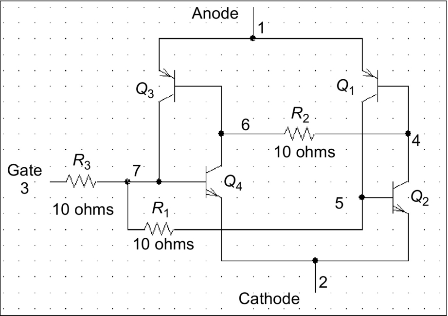
3.6.1.6 GTO SPICModel
A GTO may be modeled with two transistors shown in Fig. 3.2. However, a GTO model [14] consisting of two thyristors, which are connected in parallel, yields improved on-state, turn-on, and turn-off characteristics. The model is shown in Fig. 3.23 with four transistors.
When the anode-to-cathode voltage VAK is positive and there is no gate voltage, the GTO model will be in the off-state like a standard thyristor. If a positive voltage (VAK) is applied to the anode with respect to the cathode and no gate pulse applied, ![]() and therefore
and therefore ![]() . Thus, no anode current will flow,
. Thus, no anode current will flow, ![]() .
.
When a small voltage is applied to the gate, then IB2 is nonzero, and therefore, both ![]() are nonzero. Thus, the internal circuit will conduct, and there will a current flow from the anode to the cathode.
are nonzero. Thus, the internal circuit will conduct, and there will a current flow from the anode to the cathode.
When a negative gate pulse is applied to the GTO model, the PNP junction near to the cathode will behave as a diode. The diode will be reverse biased since the gate voltage is negative with to the cathode. Therefore, the GTO will stop conduction.
When the anode-to-cathode voltage is negative, that is, the anode voltage is negative with respect to the cathode, the GTO model will act like a reverse biased diode. This is because the PNP transistor will see a negative voltage at the emitter and the NPN transistor will see a positive voltage at the emitter. Therefore, both transistors will be in the off-state and hence the GTO will not conduct. The SPICE subcircuit description of the GTO model will be as follows:
| Subcircuit | 1 | 2 | 3 | GTO subcircuit definition | |||
| *Terminal | Anode | Cathode | Gate | ||||
| Q1 | 5 | 4 | 1 | DMOD1 | PNP | PNP transistor with model DMOD1 | |
| Q3 | 7 | 6 | 1 | DMOD1 | PNP | ||
| Q2 | 4 | 5 | 2 | DMOD2 | NPN | PNP transistor with model DMOD2 | |
| Q4 | 6 | 7 | 2 | DMOD2 | NPN | ||
| R1 | 7 | 5 | 10 Ω | ||||
| R2 | 6 | 4 | 10 Ω | ||||
| R3 | 3 | 7 | 10 Ω | ||||
| MODEL | DMOD1 | PNP | Model statement for a PNP transistor | ||||
| MODEL | DMOD2 | NPN | Model statement for an NPN transistor | ||||
| ENDS | End of subcircuit definition | ||||||

3.6.2 MOS-Controlled Thyristors
An effort to combine the advantages of bipolar junction and field-effect structures has resulted in hybrid devices such as the IGBT and the MOS-controlled thyristor (MCT). While an IGBT is an improvement over a bipolar junction transistor (BJT) using a MOSFET to turn-on and turn-off current, an MCT is an improvement over a thyristor with a pair of MOSFETs to turn-on and turn-off current. The MCT overcomes several of the limitations of the existing power devices and promises to be a better switch for the future.
The cross section of the p-type MCT unit cell is given in Fig. 3.24. When the MCT is in its forward-blocking state and a negative gate-anode voltage is applied, an inversion layer is formed in the n-doped material that allows holes to flow laterally from the p-emitter (p-channel FET source) through the channel to the p-base (p-channel FET drain). This hole flow is the base current for the npn transistor. The n-emitter then injects electrons which are collected in the n−-base, causing the p-emitter to inject holes into the n−-base so that the pnp transistor is turned on and latches the MCT. The MCT is brought out of conduction by applying a positive gate-anode voltage. This signal creates an inversion layer that diverts electrons in the n−-base away from the p-emitter and into the heavily doped n-region at the anode. This n-channel FET current amounts to a diversion of the pnp transistor base current so that its base-emitter junction turns off. Holes are then no longer available for collection by the p-base. The elimination of this hole current (npn transistor base current) causes the npn transistor to turn off. The remaining stored charge recombines and returns the MCT to its blocking state.

The seeming variability in fabrication of the turn-off FET structure continues to limit the performance of MCTs, particularly current interruption capability, though these devices can handle two to five times the conduction current density of IGBTs. Numerical modeling and its experimental verification show that ensembles of cells are sensitive to current filamentation during turnoff. All MCT device designs suffer from the problem of current interruption capability. Turn-on is relatively simple, by comparison; both the turn-on and conduction properties of the MCT approach the one-dimensional thyristor limit.
Other variations on the MCT structure have been demonstrated, namely, the emitter switched thyristor (EST) and the dual-gate emitter switched thyristor (DG-EST) [15]. These comprise integrated lateral MOSFET structures that connect a floating thyristor n-emitter region to an n+ thyristor cathode region. The MOS channels are in series with the floating n-emitter region, allowing triggering of the thyristor with electrons from the n−-base and interruption of the current to initiate turn-off. The DG-EST behaves as a dual-mode device, with the two gates allowing an IGBT mode to operate during switching and a thyristor mode to operate in the on-state.
3.6.2.1 Equivalent Circuit and Switching Characteristics
The SCR is a four-layer pnpn device with a control gate, and applying a positive gate pulse turns it on when it is forward biased. The regenerative action in the device helps to speed up the turn-on process and to keep it in the “ON” state even after the gate pulse is removed. The MCT uses an auxiliary MOS device (PMOSFET) to turn-on, and this simplifies the gate control. The turn-on has all the characteristics of a power MOSFET. The turnoff is accomplished using another MOSFET (NMOSFET), which essentially diverts the base current of one of the BJTs and breaks the regeneration.
The transistor-level equivalent circuit of a P-channel MCT and the circuit symbol are shown in Fig. 3.25. The MCT is modeled as an SCR merged with a pair of MOSFETs. The SCR consists of the bipolar junction transistors (BJTs) Q1 and Q2, which are interconnected to provide regenerative feedback such that the transistors drive each other into saturation. Of the two MOSFETs, the PMOS located between the collector and emitter of Q2 helps to turn the SCR on, and the NMOS located across the base-emitter junction of Q2 turns it off. In the actual fabrication, each MCT is made up of a large number (~100,000) cells, each of which contains a wide-base npn transistor and a narrow-base pnp transistor. While each pnp transistor in a cell is provided with an N-channel MOSFET across its emitter and base, only a small percentage (~4%) of pnp transistors are provided with P-channel MOSFETs across their emitters and collectors. The small percentage of PMOS cells in an MCT provides just enough current for turn-on and the large number of NMOS cells provide plenty of current for turnoff.
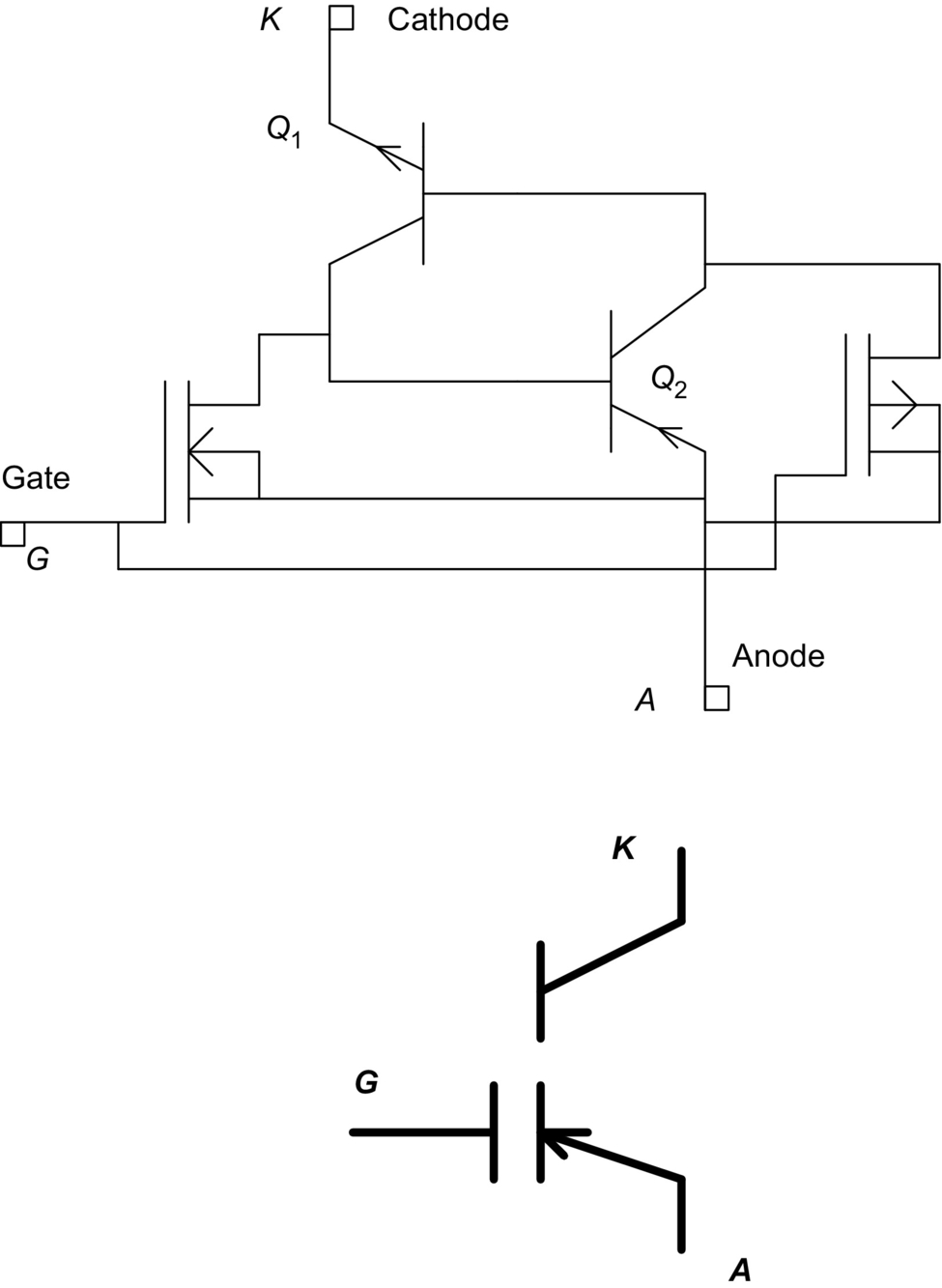
3.6.2.2 Turn-On and Turn-Off
When the MCT is in the forward-blocking state, it can be turned on by applying a negative pulse to its gate with respect to the anode. The negative pulse turns on the PMOSFET (On-FET) whose drain current flows through the base-emitter junction of Q1 (npn), thereby turning it on. The regenerative action within ![]() turns the MCT on into full conduction within a very short time and maintains it even after the gate pulse is removed. The MCT turns on without a plasma spreading phase, giving a high di/dt capability and ease of overcurrent protection. The on-state resistance of an MCT is slightly higher than that of an equivalent thyristor because of the degradation of the injection efficiency of the n+-emitter/p-base junction. Also, the peak current rating of an MCT is much higher than its average or rms current rating.
turns the MCT on into full conduction within a very short time and maintains it even after the gate pulse is removed. The MCT turns on without a plasma spreading phase, giving a high di/dt capability and ease of overcurrent protection. The on-state resistance of an MCT is slightly higher than that of an equivalent thyristor because of the degradation of the injection efficiency of the n+-emitter/p-base junction. Also, the peak current rating of an MCT is much higher than its average or rms current rating.
An MCT will remain in the “ON” state until the device current is reversed or a turn-off pulse is applied to its gate. Applying a positive pulse to its gate turns off a conducting MCT. The positive pulse turns on the NMOSFET (Off-FET), thereby diverting the base current of Q2 (pnp) away to the anode of the MCT and breaking the latching action of the SCR. This stops the regenerative feedback within the SCR and turns the MCT off. All the cells within the device are to be turned off at the same time to avoid a sudden increase in current density. When the Off-FETs are turned on, the SCR section is heavily shorted and this results in a high dv/dt rating for the MCT. The highest current that can be turned off with the application of a gate bias is called the “maximum controllable current.” The MCT can be gate controlled if the device current is less than the maximum controllable current. For smaller device currents, the width of the turn-off pulse is not critical. However, for larger currents, the gate pulse has to be wider and more often has to occupy the entire off-period of the switch.
3.6.2.3 Comparison of MCT and Other Power Devices
An MCT can be compared with a power MOSFET, a power BJT, and an IGBT of similar voltage and current ratings. The operation of the devices is compared under on-state, off-state, and transient conditions. The comparison is simple and very comprehensive.
The current density of an MCT is ![]() 70% higher than that of an IGBT having the same total current [16]. During its on-state, an MCT has a lower conduction drop compared with other devices. This is attributed to the reduced cell size and the absence of emitter shorts present in the SCR within the MCT. The MCT also has a modest negative temperature coefficient at lower currents with the temperature coefficient turning positive at larger current [16]. Fig. 3.26 shows the conduction drop as a function of current density. The forward drop of a 50 A MCT at 25°C is around 1.1 V, while that for a comparable IGBT is over 2.5 V. The equivalent voltage drop calculated from the value of rDS(ON) for a power MOSFET will be much higher. However, the power MOSFET has a much lower delay time (30 ns) compared with that of an MCT (300 ns). The turn-on of a power MOSFET can be so much faster than an MCT or an IGBT; therefore, the switching losses would be negligible compared with the conduction losses. The turn-on of an IGBT is intentionally slowed down to control the reverse recovery of the freewheeling diode used in inductive switching circuits [17].
70% higher than that of an IGBT having the same total current [16]. During its on-state, an MCT has a lower conduction drop compared with other devices. This is attributed to the reduced cell size and the absence of emitter shorts present in the SCR within the MCT. The MCT also has a modest negative temperature coefficient at lower currents with the temperature coefficient turning positive at larger current [16]. Fig. 3.26 shows the conduction drop as a function of current density. The forward drop of a 50 A MCT at 25°C is around 1.1 V, while that for a comparable IGBT is over 2.5 V. The equivalent voltage drop calculated from the value of rDS(ON) for a power MOSFET will be much higher. However, the power MOSFET has a much lower delay time (30 ns) compared with that of an MCT (300 ns). The turn-on of a power MOSFET can be so much faster than an MCT or an IGBT; therefore, the switching losses would be negligible compared with the conduction losses. The turn-on of an IGBT is intentionally slowed down to control the reverse recovery of the freewheeling diode used in inductive switching circuits [17].

The MCT can be manufactured for a wide range of blocking voltages. Turn-off speeds of MCTs are supposed to be higher as initially predicted. The turn-on performance of Generation-2 MCTs is reported to be better compared with Generation-1 devices. Even though the Generation-1 MCTs have higher turn-off times compared with IGBTs, the newer ones with higher radiation (hardening) dosage have comparable turn-off times. At present, extensive development activity in IGBTs has resulted in high-speed switched mode power supply (SMPS) IGBTs that can operate at switching speeds ![]() 150 kHz [18]. The turn-off delay time and the fall time for an MCT are much higher compared with a power MOSFET, and they are found to increase with temperature [16]. Power MOSFETs become attractive at switching frequencies above 200 kHz, and they have the lowest turn-off losses among the three devices.
150 kHz [18]. The turn-off delay time and the fall time for an MCT are much higher compared with a power MOSFET, and they are found to increase with temperature [16]. Power MOSFETs become attractive at switching frequencies above 200 kHz, and they have the lowest turn-off losses among the three devices.
The turn-off safe operating area (SOA) is better in the case of an IGBT than an MCT. For an MCT, the full switching current is sustainable at ![]() 50%–60% of the breakdown voltage rating, while for an IGBT, it is about 80%. The use of capacitive snubbers becomes necessary to shape the turn-off locus of an MCT. The addition of even a small capacitor improves the SOA considerably.
50%–60% of the breakdown voltage rating, while for an IGBT, it is about 80%. The use of capacitive snubbers becomes necessary to shape the turn-off locus of an MCT. The addition of even a small capacitor improves the SOA considerably.
The MCT has a MOS gate similar to a power MOSFET or an IGBT, and hence, it is easy to control. In a PMCT, the gate voltage must be applied with respect to its anode. A negative voltage below the threshold of the On-FET must be applied to turn on the MCT. The gate voltage should fall within the specified steady-state limits in order to give a reasonably low delay time and to avoid any gate damage due to overvoltage [17]. Similar to a GTO, the gate voltage rise time has to be limited to avoid hot spots (current crowding) in the MCT cells. A gate voltage less than −5 V for turnoff and greater than 10 V for turn-on ensures proper operation of the MCT. The latching of the MCT requires that the gate voltage be held at a positive level in order to keep the MCT turned off.
Because the peak-to-peak voltage levels required for driving the MCT exceed those of other gate-controlled devices, the use of commercial drivers is limited. The MCT can be turned on and off using a push-pull pair with discrete NMOS-PMOS devices, which, in turn, are driven by commercial integrated circuits (ICs). However, some drivers developed by MCT manufacturers are not commercially available [17].
A Baker's clamp push-pull can also be used to generate gate pulses of negative and positive polarity of adjustable width for driving the MCT [19–21]. The Baker's clamp ensures that the push-pull transistors will be in the quasisaturated state prior to turnoff, and this results in a fast switching action. Also, the negative feedback built into the circuit ensures satisfactory operation against variations in load and temperature. A similar circuit with a push-pull transistor pair in parallel with a pair of power BJTs is available [22]. An intermediate section, with a BJT that is either cut off or saturated, provides −10 V and +15 V through potential division.
3.6.2.4 Protection of MCTs
Paralleling of MCTs
Similar to power MOSFETs, MCTs can be operated in parallel. Several MCTs can be paralleled to form larger modules with only slight derating of the individual devices provided the devices are matched for proper current sharing. In particular, the forward voltage drops of individual devices have to be matched closely.
Overcurrent protection
The anode-to-cathode voltage in an MCT increases with its anode current, and this property can be used to develop a protection scheme against overcurrent [19,20]. The gate pulses to the MCT are blocked when the anode current and hence the anode-to-cathode voltage exceed a preset value. A Schmitt trigger comparator is used to allow gate pulses to the MCT when it is in the process of turning on, during which time the anode voltage is relatively large and decreasing.
Snubbers
As with any other power device, the MCT is to be protected against switching-induced transient voltage and current spikes by using suitable snubbers. The snubbers modify the voltage and current transients during switching such that the switching trajectory is confined within the SOA. When the MCT is operated at high frequencies, the snubber increases the switching loss due to the delayed voltage and current responses. The power circuit of an MCT chopper including an improved snubber circuit is shown in Fig. 3.27 [19,21]. The turn-on snubber consists of Ls and DLS, and the turn-off snubber consists of Rs,Cs,andDLS. The series-connected turn-on snubber reduces the rate of change of the anode current dlA/dt. The MCT does not support Vs until the current through the freewheeling diode reaches zero at turn-on. The turn-off snubber helps to reduce the peak power and the total power dissipated by the MCT by reducing the voltage across the MCT when the anode current decays to zero. The analysis and design of the snubber and the effect of the snubber on switching loss and EMI are given in Refs. [19] and [21]. An alternative snubber configuration for the two MCTs in an ac-ac converter has also been reported [22]. This snubber uses only one capacitor and one inductor for both the MCT switches (PMCT and NMCT) in a power-converter leg.
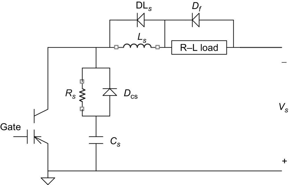
Simulation model of an MCT
The operation of power converters can be analyzed using PSPICE and other simulation software. As it is a new device, models of MCTs are not provided as part of the simulation libraries. However, an appropriate model for the MCT would be helpful in predicting the performance of novel converter topologies and in designing the control and protection circuits. Such a model must be simple enough to keep the simulation time and effort at a minimum and must represent most of the device properties that affect the circuit operation. The PSPICE models for Harris PMCTs are provided by the manufacturer and can be downloaded from the internet. However, a simple model presenting most of the characteristics of an MCT is available [23,24]. It is derived from the transistor-level equivalent circuit of the MCT by expanding the SCR model already reported the literature. The improved model [24] is capable of simulating the breakover and breakdown characteristics of an MCT and can be used for the simulation of high-frequency converters.
3.6.3 Generation-1 and Generation-2 MCTs
The Generation-1 MCTs were commercially introduced by Harris Semiconductors in 1992. However, the development of Generation-2 MCTs is continuing. In Gen-2 MCTs, each cell has its own turn-on field-effect transistor (FET). Preliminary test results in Generation-2 devices and a comparison of their performance with those of Generation-1 devices and high-speed IGBTs are available [25,26]. The Generation-2 MCTs have a lower forward drop compared with the Generation-1 MCTs. They also have a higher di/dt rating for a given value of capacitor used for discharge. During hard switching, the fall time and the switching losses are lower for the Gen-2 MCTs. The Gen-2 MCTs have the same conduction loss characteristics as Gen-1 with drastic reductions in turn-off switching times and losses [27].
Under zero-current switching conditions, Gen-2 MCTs have negligible switching losses [27]. Under zero-voltage switching, the turn-off losses in a Gen-2 device are one-half to one-fourth (depending on temperature and current level) the turn-off losses in Gen-1 devices. In all soft-switching applications, the predominant loss, namely, the conduction loss, reduces drastically allowing the use of fewer switches in a module.
3.6.4 N-channel MCT
The PMCT discussed in this chapter uses an NMOSFET for turnoff, and this results in a higher turn-off current capability. The PMCT can only replace a P-channel IGBT and inherits all the limitations of a P-channel IGBT. The results of a 2-D simulation show that the NMCT can have a higher controllable current [27]. It is reported that NMCT versions of almost all Harris PMCTs have been fabricated for analyzing the potential for a commercial product [17]. The NMCTs are also being evaluated for use in zero-current soft-switching applications. However, the initial results are not quite encouraging in that the peak turn-off current of an NMCT is one-half to one-third of the value achievable in a PMCT. It is hoped that the NMCTs will eventually have a lower switching loss and a larger SOA as compared with PMCTs and IGBTs.
3.6.5 Base Resistance-Controlled Thyristor [28]
The base resistance-controlled thyristor (BRT) is another gate-controlled device that is similar to the MCT but with a different structure. The Off-FET is not integrated within the p-base region but is formed within the n−-base region. The diverter region is a shallow p-type junction formed adjacent to the p-base region of the thyristor. The fabrication process is simpler for this type of structure. The transistor-level equivalent circuit of a BRT is shown in Fig. 3.28.

The BRT will be in the forward-blocking state with a positive voltage applied to the anode and with a zero gate bias. The forward-blocking voltage will be equal to the breakdown voltage of the open-base pnp transistor. A positive gate bias turns on the BRT. At low current levels, the device behaves similarly to an IGBT. When the anode current increases, the operation changes to thyristor mode resulting in a low forward drop. Applying a negative voltage to its gate turns off the BRT. During the turn-off process, the anode current is diverted from the n+ emitter to the diverter. The BRT has a current tail during turnoff that is similar to an MCT or an IGBT.
3.6.6 MOS Turn-off Thyristor [29]
The MOS turn-off (MTO) thyristor or the MTOT is a replacement for the GTO and it requires a much smaller gate drive. It is more efficient than a GTO; it can have a maximum blocking voltage of about 9 kV, and it will be used to build power converters in the 1–20 MVA range. Silicon Power Corporation (SPCO) manufactures the device.
The transistor-level equivalent circuit of the MTOT (hybrid design) and the circuit symbol are shown in Fig. 3.29. Applying a current pulse at the turn-on gate (Gl), as with a conventional GTO, turns on the MTOT. The turn-on action, including regeneration, is similar to a conventional SCR. Applying a positive voltage pulse to the turn-off gate (G2), as with an MCT, turns off the MTOT. The voltage pulse turns on the FET, thereby shorting the emitter and base of the npn transistor and breaking the regenerative action. The MTOT is a faster switch than a GTO in that it is turned off with a reduced storage time compared with a GTO. The disk-type construction allows double-sided cooling.

3.6.7 Static Induction Thyristors
An SITh or FCTh has a cross section similar to that shown in Fig. 3.30. Other SITh configurations have surface-gate structures. The device is essentially a pin diode with a gate structure that can pinch-off anode current flow. High-power SIThs have a subsurface gate (buried-gate) structure to allow larger cathode areas to be utilized, and hence, larger current densities are possible.

Planar gate devices have been fabricated with blocking capabilities of up to 1.2 kV and conduction currents of 200 A, while step-gate (trench-gate) structures have been produced that are able to block up to 4 kV and conduct 400 A. Similar devices with a “Verigrid” structure have been demonstrated that can block 2 kV and conduct 200 A, with claims of up to 3.5 kV blocking and 200 A conduction. Buried-gate devices that block 2.5 kV and conduct 300 A have also been fabricated. Recently, there has been a resurgence of interest in these devices for fabrication in SiC.
3.6.8 Optically Triggered Thyristors
Optically gated thyristors have traditionally been used in power utility applications where series stacks of devices are necessary to achieve the high voltages required. Isolation between gate-drive circuits for circuits such as static VAR compensators and high-voltage dc-ac inverters (for use in high-voltage dc (HVDC) transmission) has driven the development of this class of devices, which are typically available in ratings from 5 to 8 kV. The cross section is similar to that shown in Fig. 3.31, showing the photosensitive region and the amplifying gate structures. Light-triggered thyristors (LTTs) may also integrate overvoltage protection.

One of the most recent devices can block 6 kV forward and reverse, conduct 2.5 kA average current, and maintain a di/dt capability of 300 A/μs and a dv/dt capability of 3000 V/μs, with a required trigger power of 10 mW. An integrated light-triggered and light-quenched SITh has been produced that can block 1.2 kV and conduct up to 20 A (at a forward drop of 2.5 V). This device is an integration of a normally off buried-gate static induction photo-thyristor and a normally off p-channel darlington surface-gate static induction phototransistor. The optical trigger and quenching power required is less than 5 and 0.2 mW, respectively.
3.6.9 Bi-directional Controlled Thyristors
The BCT is an integrated assembly of two antiparallel thyristors on one Si wafer. The intended applications for this switch are VAR compensators, static switches, soft starters, and motor drives. These devices are rated up to 6.5 kV blocking. Cross talk between the two halves has been minimized. A cross section of the BCT is shown in Fig. 3.32. Note that each surface has a cathode and an anode (opposite devices). The small gate-cathode periphery necessarily restricts the BCT to low-frequency applications because of its di/dt limit.

Low-power devices similar to the BCT, but in existence for many years, are the diac and triac. A simplified cross section of a diac is shown in Fig. 3.33. A positive voltage applied to the anode with respect to the cathode forward biases J1, while reverse biasing J2. J4 and J3 are shorted by the metal contacts. When J2 is biased to breakdown, a lateral current flows in the p2 region. This lateral flow forward biases the edge of J3, causing carrier injection. The result is that the device switches into its thyristor mode and latches. Applying a reverse voltage causes the opposite behavior at each junction, but with the same result. Fig. 3.33 also shows the i-v plot for a diac.

The addition of a gate connection, to form a triac, allows the breakover to be controlled at a lower forward voltage. Fig. 3.34 shows the structure for the triac. Unlike the diac, this is not symmetrical, resulting in differing forward and reverse breakover voltages for a given gate voltage. The device is fired by applying a gate pulse of the same polarity relative to MT1 as that of MT2.

3.7 Gate Drive Requirements
3.7.1 Snubber Circuits
To protect a thyristor, from a large di/dt during turn-on and a large dv/dt during turnoff, a snubber circuit is needed. A general snubber topology is shown in Fig. 3.35. The turn-on snubber is made by inductance L1 (often, L1 is stray inductance only). This protects the thyristor from a large di/dt during the turn-on process. The auxiliary circuit made by R1 and D1 allows the discharging of L1 when the thyristor is turned off. The turn-off snubber is made by resistor R2 and capacitance C2. This circuit protects a GTO from large dv/dt during the turn-off process. The auxiliary circuit made by D2 and R2 allows the discharging of C2 when the thyristor is turned on. The circuit of capacitance C2 and inductance L1 also limits the value of dv/dt across the thyristor during forward-blocking. In addition, L1 protects the thyristor from reverse overcurrents. R1 and diodes D1,D2, are usually omitted in ac circuits with converter-grade thyristors. A similar second set of L, C, and R may be used around this circuit in HVDC applications.

3.7.2 Gate Circuits
It is possible to turn on a thyristor by injecting a current pulse into its gate. This process is known as gating, triggering, or firing the thyristor. The most important restrictions are on the maximum peak and duration of the gate pulse current. In order to allow a fast turn-on and a correspondingly large anode di/dt during the turn-on process, a large gate current pulse is supplied during the initial turn-on phase with a large diG/dt. The gate current is kept on, at lower value, for some times after the thyristor turned on in order to avoid unwanted turn-off of the device; this is known as the “back-porch” current. A shaped gate current waveform of this type is shown in Fig. 3.36.
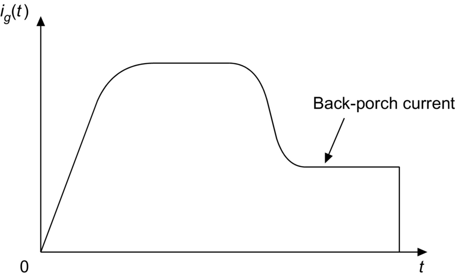
Fig. 3.37 shows typical gate i-v characteristics for the maximum and minimum operating temperatures. The dashed line represents the minimum gate current and corresponding gate voltage needed to ensure that the thyristor will be triggered at various operating temperatures. It is also known as the locus of minimum firing points. On the data sheet, it is possible find a line representing the maximum operating power of the thyristor gating internal circuit. The straight line, between VGG and VGG/RG, represents the current voltage characteristic of the equivalent trigger circuit. If the equivalent trigger circuit line intercepts the two gate i-v characteristics for the maximum and minimum operating temperatures between where they intercept the dashed lines (minimum gate current to trigger and maximum gate power dissipation), then the trigger circuit is able to turn-on the thyristor at any operating temperature without destroying or damaging the device.
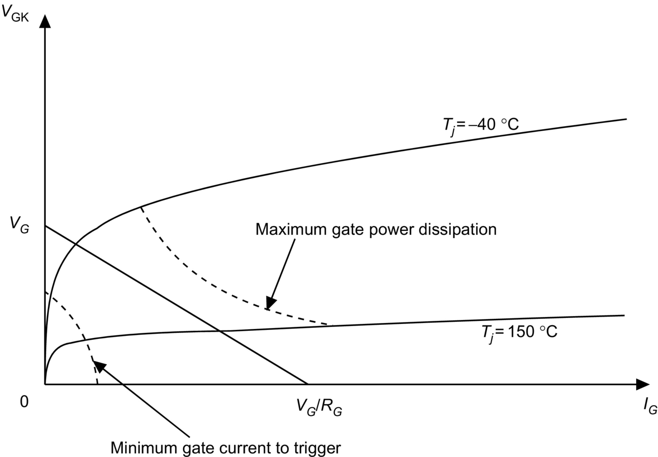
In order to keep the power circuit and the control circuit electrically unconnected, the gate signal generator and the gate of the thyristor are often connected through a transformer. There is a transformer winding for each thyristor, and in this way, unwanted short circuits between devices are avoided. A general block diagram of a thyristor gate trigger circuit is shown in Fig. 3.38. This application is for a standard bridge configuration often used in power converters.
Another problem can arise if the load impedance is high, particularly if the load is inductive and the supply voltage is low. In this situation, the latching current may not be reached during the trigger pulse. A possible solution to this problem could be the use of a longer current pulse. However, such a solution is not attractive because of the presence of the isolation transformer. An alternative solution is the generation of a series of short pulses that last for the same duration as a single long pulse. A single short pulse, a single long pulse, and a series of short pulses are shown in Fig. 3.39. Reliable gating of the thyristor is essential in many applications.

There are many gate trigger circuits that use optical isolation between the logic-level electronics and a drive stage (typically MOSFETs) configured in a push-pull output. The dc power supply voltage for the drive stage is provided through transformer isolation. Many device manufacturers supply drive circuits available on printed circuit (PC) boards or diagrams of suggested circuits.
IGCT gate drives consist of an integrated module to which the thyristor is connected via a low-inductance mounting; an example is given in Fig. 3.40. Multiple MOSFETs and capacitors connected in parallel may be used to source or sink the necessary currents to turn the device on or off. Logic in the module controls the gate drive from a fiber-optic trigger input and provides diagnostic feedback from a fiber-optic output. A simple power supply connection is also required.
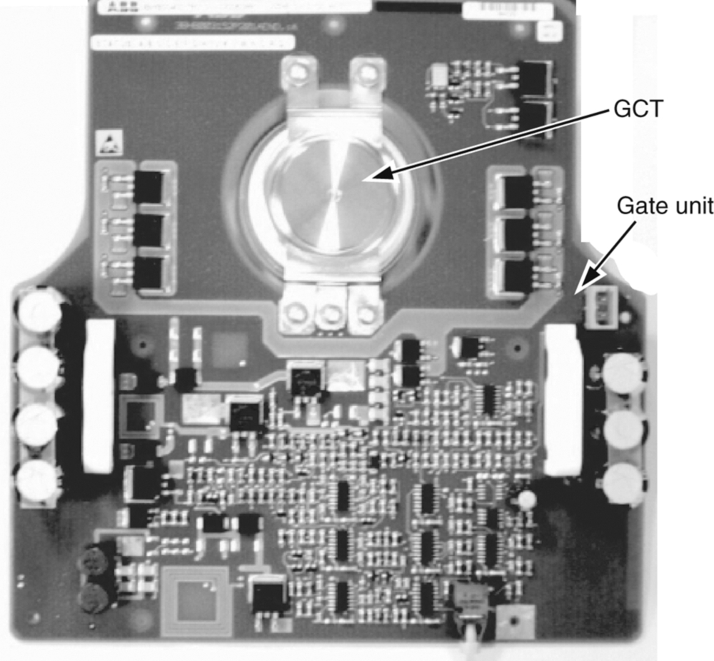
Values for each cell of a multicell GTO model
| Model component | Symbol | Value |
| Delay resistor | R | 1 μΩ |
| Delay capacitor | C | 1 nF |
| Mutual coupling inductance | M | 10 nH |
| Gate contact resistance | RGC | 1 mΩ |
| Cathode contact resistance | RKC | 1 mΩ |
Other GTO thyristor models have been developed that offer improved accuracy at the expense of increased complexity. The model by Tseng et al. [30] includes charge storage effects in the n−-base, and its application to a multicell model, as in Fig. 3.14, has been demonstrated successfully. Models for the IGCT, based on the lumped-charge approach [31] and the Fourier-based solution of the ambipolar diffusion equation (ADE) [32], have also been developed.
3.8 Applications
The most important application of thyristors is for line-frequency phase-controlled rectifiers. This family includes several topologies, of which one of the most important is used to construct HVDC transmission systems. A single-phase controlled rectifier is shown in Fig. 3.41.

The use of thyristors instead of diodes allows the average output voltage to be controlled by appropriate gating of the thyristors. If the gate signals to the thyristors were continuously applied, the thyristors in Fig. 3.41 would behave as diodes. If no gate currents are supplied, they behave as open circuits. Gate current can be applied any time (phase delay) after the forward voltage becomes positive. Using this phase-control feature, it is possible to produce an average dc output voltage less than the average output voltage obtained from an uncontrolled diode rectifier.
3.8.1 DC–AC Utility Inverters
Three-phase converters can be made in different ways, according to the system in which they are employed. The basic circuit used to construct these topologies—the three-phase controlled rectifier—is shown in Fig. 3.42.
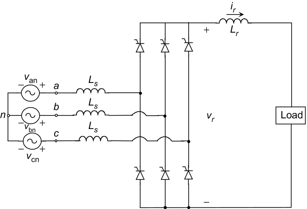
Starting from this basic configuration, it is possible to construct more complex circuits in order to obtain high-voltage or high-current outputs or just to reduce the output ripple by constructing a multiphase converter. One of the most important systems using the topology shown in Fig. 3.42 as a basic circuit is the HVDC system represented in Fig. 3.43. This system is made by two converters, a transmission line, and two ac systems. Each converter terminal is made of two poles. Each pole is made by two six-pulse line-frequency converters connected through Δ–Y and Y–Y transformers in order to obtain a 12-pulse converter and a reduced output ripple. The filters are required to reduce the current harmonics generated by the converter.

When a large amount of current and relatively low voltage is required, it is possible to connect in parallel, using a specially designed inductor, two six-pulse line-frequency converters connected through Δ–Y and Y–Y transformers. The special inductor is designed to absorb the voltage between the two converters and to provide a pole to the load. This topology is shown in Fig. 3.44. This configuration is often known as a 12-pulse converter. Higher pulse numbers may also be found.
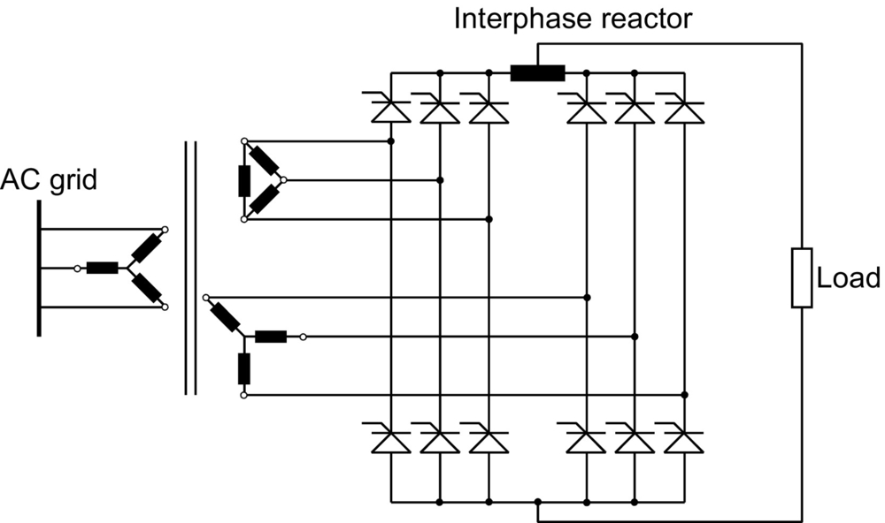
3.8.2 Motor Control
Another important application of thyristors is in motor control circuits. Historically, thyristors have been used heavily in traction, although most new designs are now based on IGBTs. Such motor control circuits broadly fall into four types: (i) chopper control of a dc motor from a dc supply, (ii) single- or three-phase converter control of a dc motor from an ac supply, (iii) inverter control of an ac synchronous or induction machine from a dc supply, and (iv) cycloconverter control of an ac machine from an ac supply. An example of a GTO chopper is given in Fig. 3.45. L1,R1,D1,andC1 are the turn-on snubber; R2,D2,andC2 are the turn-off snubber; finally, R3andD3 form the snubber for the freewheel diode D3. A thyristor cycloconverter is shown in Fig. 3.46; the waveforms show the fundamental component of the output voltage for one phase. Three double converters are used to produce a three-phase variable-frequency, variable voltage sinusoidal output for driving ac motors. However, the limited frequency range (less than a third of the line frequency) restricts the application to large, low-speed machines at high powers.


A single- or three-phase thyristor converter (controlled rectifier) may be used to provide a variable dc supply for controlling a dc motor. Such a converter may also be used as the front end of a three-phase induction motor drive. The variable voltage, variable-frequency motor drive requires a dc supply, which is supplied by the thyristor converter. The drive may use a square wave or PWM voltage source inverter (VSI) or a current source inverter (CSI). Fig. 3.47 shows a square wave or PWM VSI with a controlled rectifier on the input side. The switch block inverter may be made of thyristors (usually GTOs or IGCTs) for high power, although most new designs now use IGBTs. Low-power motor controllers generally use IGBT inverters.

In motor control, thyristors are also used in CSI topologies. When the motor is controlled by a CSI, a controlled rectifier is also needed on the input side. Fig. 3.48 shows a typical CSI inverter. The capacitors are needed to force the current in the thyristors to zero at each switching event. This is not needed when using GTOs. This inverter topology does not need any additional circuitry to provide the regenerative braking (energy recovery when slowing the motor). Historically, two back-to-back connected line-frequency thyristor converters have been employed to allow bidirectional power flow and thus regenerative braking. Use of antiparallel GTOs with symmetrical blocking capability, or the use of diodes in series with each asymmetrical GTO, reduces the number of power devices needed, but greatly increases the control complexity.

3.8.3 VAR Compensators and Static Switching Systems
Thyristors are also used to switch capacitors or inductors in order to control the reactive power in the system. Such arrangements may also be used in phase-balancing circuits for balancing the load fed from a three-phase supply. Examples of these circuits are shown in Fig. 3.49. These circuits act as static VAR controllers. The topology represented on the left of Fig. 3.49 is called a thyristor-controlled inductor (TCI), and it acts as a variable inductor where the inductive VAR supplied can be varied quickly. Because the system may require either inductive or capacitive VAR compensation, it is possible to connect a bank of capacitors in parallel with a TCI. The topology shown on the right of Fig. 3.49 is called a thyristor-switched capacitor (TSC). Capacitors can be switched out by blocking the gate pulse of all thyristors in the circuit. The problem of this topology is the voltage across the capacitors at the thyristor turnoff. At turn-on the thyristor must be gated at the instant of the maximum ac voltage to avoid large overcurrents. Many recent SVCs have used GTOs.

A similar application of thyristors is in solid-state fault current limiters and circuit breakers. In normal operation, the thyristors are continuously gated. However, under fault conditions, they are switched rapidly to increase the series impedance in the load and to limit the fault current. Key advantages are the flexibility of the current limiting, which is independent of the location of the fault and the change in load impedance, the reduction in fault level of the supply, and a smaller voltage sag during a short-circuit fault.
A less important application of thyristors is as a static transfer switch, used to improve the reliability of uninterruptible power supplies (UPS) as shown in Fig. 3.50. There are two modes of using the thyristors. The first leaves the load permanently connected to the UPS system and in case of emergency disconnects the load from the UPS and connects it directly to the power line. The second mode is opposite to the first one. Under normal conditions, the load is permanently connected to the power line, and in event of a line outage, the load is disconnected from the power line and connected to the UPS system.
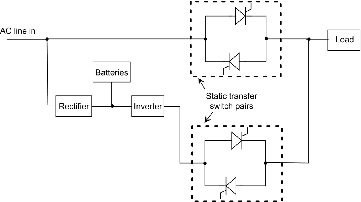
3.8.4 Lighting Control Circuits
An important circuit used in lighting control is the dimmer, based on a triac and shown in Fig. 3.51. The R-C network applies a phase shift to the gate voltage, delaying the triggering of the triac. Varying the resistance controls the firing angle of the triac and therefore the voltage across the load. The diac is used to provide symmetrical triggering for the positive and negative half cycles, due to the nonsymmetrical nature of the triac. This ensures symmetrical waveforms and elimination of even harmonics. An L-C filter is often used to reduce any remaining harmonics.