
5.3.4 SiC JFET
The SiC JFET has some benefits, such as a resistive forward characteristic in the first and third quadrants and a monolithic integrated body diode. It is comparable with available SiC Schottky diodes in terms of stored charge, low output capacitance, low gate charge, and low switching losses that makes it attractive for use.
The first commercialized SiC transistor was normally the ON JFET from SemiSouth Laboratories and SiCED Electronics Development. They were easy to implement as there were no reliability issues with gate oxide as with SiC MOSFETs. The JFETs are only depletion-mode, normally ON-type devices that conduct current at zero gate voltage and are fully blocked when the gate voltage is below the pinch-off voltage. The most successful JFET type, in terms of voltage and current ratings, has been the lateral channel JFET (LCJFET), shown in Fig. 5.8 The LCJFET allows optimization of the channel parameters and is easy to fabricate. Due to the combined lateral-vertical channel design, the LCJFET has significantly reduced Miller capacitance. A parasitic diode formed with the buried P region and the N drift region can be used as a freewheeling diode without an external antiparallel diode. Also, the current through the channels can flow in the reverse direction when enough gate-source voltage is applied; therefore, the LCJFET can work in synchronous rectification circuits.

When JFETs are ON, they exhibit constant resistance that can be minimized by increasing the gate voltage slightly higher than zero. A normally-ON device is not easy to use in a power application because losing the control can cause undesired conduction of the switch and, consequently, can lead to shoot-through current damaging the circuit [97].
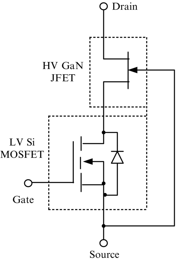
A cascode configuration, shown in Fig. 5.9, composed of a SiC JFET and a series-connected low-voltage Si MOSFET, can overcome the problem and make a normally-ON JFET behave similarly to a conventional MOSFET. Typically, a 30 V MOSFET with very low ON-resistance controls the JFET conduction. When the two devices are conducting, the conduction losses of the MOSFET will be insignificant. When the Si MOSFET is turned on, the gate-source voltage of the JFET becomes zero, allowing current to pass from the drain to the source. The forward characteristics of a cascode configuration are determined by the gate-source voltage applied to the MOSFET.
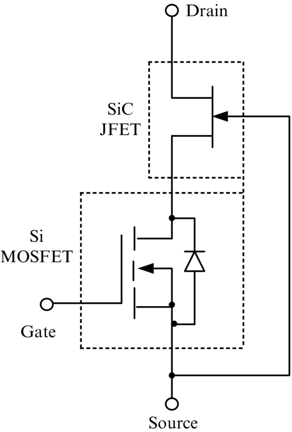
During the OFF-state, the cascode exhibits a rugged avalanche behavior. Since in a cascode configuration the control device is a low-voltage Si MOSFET, it is easy to replace a power device with a cascode configuration packed as one device, because the control is made with the same voltage levels. The temperature coefficient of the ON-resistance of a SiC JFET is positive, which naturally protects the device from overshooting during high-temperature operation. However, there are some limitations with a cascode configuration. The maximum operating temperature in a cascode configuration is limited by the Si MOSFET, the Si MOSFET internal body diode shows a low dv/dt rating, limiting the switching frequency of the JFET, and the conduction losses are higher since the two devices are connected in series [98].
To overcome these limitations, gate drivers that can block a JFET have been designed. The driver output voltage swings from zero to negative voltage. The negative voltage level is less than the maximum pinch-off voltage of the device and, therefore, could cause a gate avalanche condition. In order to limit uncontrolled avalanche current, a parallel circuit, that includes a resistor, capacitor, and diode connected in series to the JFET gate, can be used. This parallel circuit is capable of limiting the avalanche current but supplying the high gate current peaks required for fast switching [99]. A disadvantage of using a special JFET driver is that a negative supply voltage should be provided to the drive circuit that complicates the control circuit of the device. Also, replacing a power device with a JFET in a power application is more complicated because the driver and the control are also affected.
In 2011, normally OFF vertical channel JFETs (VCJFETs) compatible with standard gate drive circuitry and featuring a positive temperature coefficient for ease in paralleling were commercially available. VCJFETs were based on a patented vertical channel trench structure from SemiSouth Laboratories, Inc. A typical high-voltage VCJFET is shown in Fig. 5.10.

When the channel voltage is smaller (VCH<VCHsat), a VCJFET works in the linear region and has an approximately constant ON-state resistance; the value of which is the sum of the channel and drift region resistance. The drain current, ID, can be calculated by the following equation [100]:
where IP is the pinch-off current depending on the channel parameters, such as electron mobility, μn; doping concentration, NCH; VCJFET thickness, Z; half of the width of the channel region, a; and the effective length of the channel. The pinch-off current is calculated by the following equation:
Since the drift region of a high-voltage SiC VCJFET is designed to support high voltage, the drift region is thick and lightly doped. Hence, the drift resistance will be significantly higher than other resistance through which the drain current is flowing. Therefore, the drift resistance should be included for calculating the channel voltage, VCH:
where RDrift is the drift resistance. To simplify the expression for calculating the drift resistance, the current spreading effect of the current coming from the channel can be neglected; then, the drift resistance can be calculated as the resistance of the rectangular area in the drift region under the channel:

where LDrift and WDrift are the drift region thickness and the width and NDrift is the doping concentration of the lightly doped drift region.
The pinch-off voltage depends on the channel parameters and can be calculated by the equation:
The built-in voltage is

where NP is the doping concentration of the gate.
When the channel voltage is increased so that VCH>VCHsat, the drain current saturates. The saturation current is defined by the following equation:
There are two reasons for the drain current to saturate. One reason is that the depletion region becomes progressively wider toward the drain side causing a reduction of channel width and an increase of channel resistance. The other reason is that due to the presence of a high electric field in the channel, the carrier velocity saturates. The saturated drain current, IDSAT, can be calculated by the equation [100]:

The multiplication term ![]() in Eq. (5.96) is used to account for the channel modulation effect.
in Eq. (5.96) is used to account for the channel modulation effect.
A benefit of a VCJFET is that it can be used in directions, forward and reverse, in a converter circuit. The reverse I–V characteristics do not saturate as do the forward I–V characteristics. The reason for this is that when the drain current is in the reverse direction, VGD>VGS, the channel closes so the drain side will be wide open. As a result, as VSD increases, the channel is never pinched off when VGS>Vth, while when VGS<Vth, the channel is always pinched off on the side of the source and wide open on the drain side. Therefore, it is possible for a VCJFET to be used for freewheeling, although no parasitic diode is formed between the source and the drain [101].
In order to model the switching losses of a VCJFET, the capacitance between gate and source, CGS, and the capacitance between gate and drain, CGD, should be known. The gate-source capacitance is
where KGS is the coupling area, the coefficient of the gate and source; AGS is the coupling area between gate and source; and WS is the depletion width between the gate and source. The depletion width can be calculated by
The gate-to-drain capacitance is
where the width of the depletion region between the gate and the drain is

Some of the parameters of SiC JFETs and MOSFETs are presented in Table 5.7 as their switching losses FOM (SLFOM) and conduction losses FOM (CLFOM). The MOSFET FOMs are smaller although the MOSFET current is higher. In 2009, it was stated that a SiC MOSFET would be the device of choice as soon as the SiO2/SiC interface and reliability issues were resolved [104]. The two companies that were producing JFETs no longer exist. Infineon Technologies discontinued their JFET products. Other SiC companies are more interested in production and development of SiC MOSFETs; therefore, the future of the SiC JFET is still unknown.

5.3.5 SiC BJT
Power BJTs in SiC are very attractive for power switching applications due to their very low specific ON-resistance and high-temperature operation with high power densities [105]. The common-emitter gain, β; the specific on-resistance, RSP_ON; and the open-base breakdown voltage, BVCEO, are important parameters that should be accounted for in choosing a device for a power application. The current gain should be high enough to reduce the base current that controls the BJT. Considerable work has been done to improve device performance. One of the main challenges is to increase the current gain of 4H-SiC BJTs [106] that is limited by the surface recombination [105]. Reducing the surface recombination current by optimizing the surface passivation improves the current gain [107]. Also, the common-emitter current gain can be improved by increasing the minority carrier lifetime in the base and emitter regions [108]. The maximum current gain for high-voltage SiC BJTs that has been reported in the literature is 335 for a 600 V device [109].
To increase the blocking voltage, the growth of high-purity SiC homoepitaxial thin films on SiC single-crystal wafers is required to form N−N+ wafer structures [110]. The maximum open-base breakdown voltage, BVCEO, for a SiC BJT was reported to be 6 kV, but the gain was only 3 [111]. Further work is necessary to improve the design and to develop a new processing technology so that an increase in BVCEO can be achieved without sacrificing the current gain of the transistor. Also, the conduction and switching power losses should be minimized. The conduction losses depend on the collector-emitter voltage and the collector current.
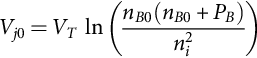
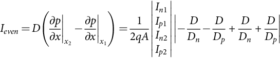
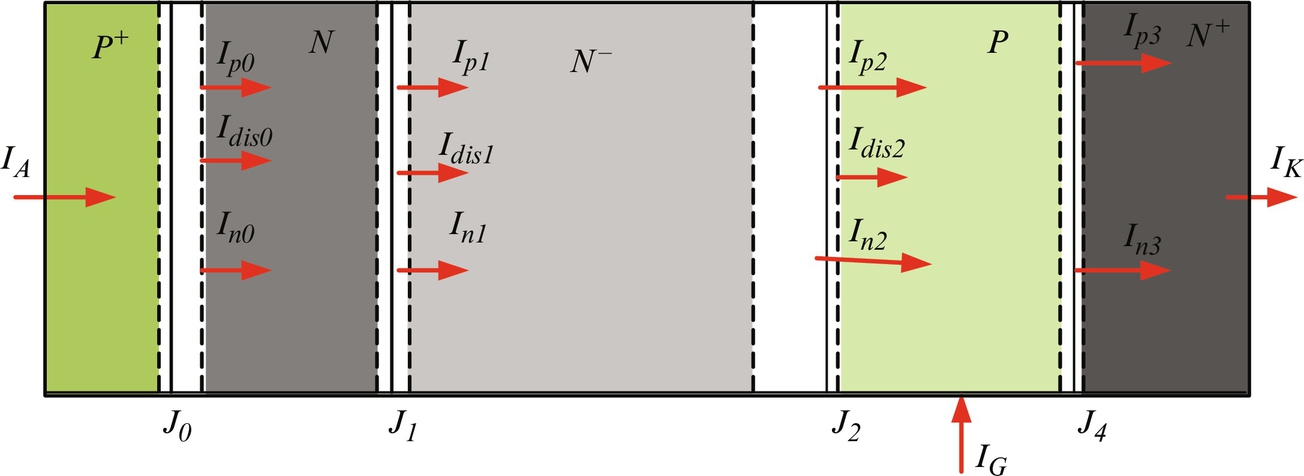
The voltage drop, VCE, across the high-power SiC BJT is composed of six components, including the voltages across the junctions, J0, J1, and pseudojunction, J2; the voltage across the two depletion regions, Vd1 and Vd2; and the voltage across the carrier storage region (CSR), ![]() :
:
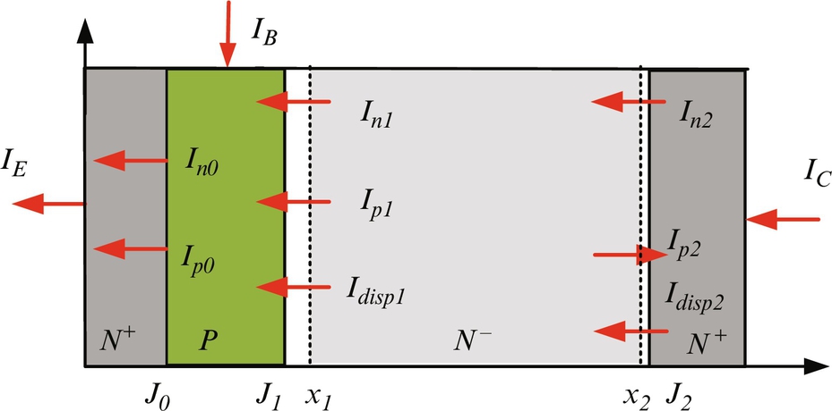
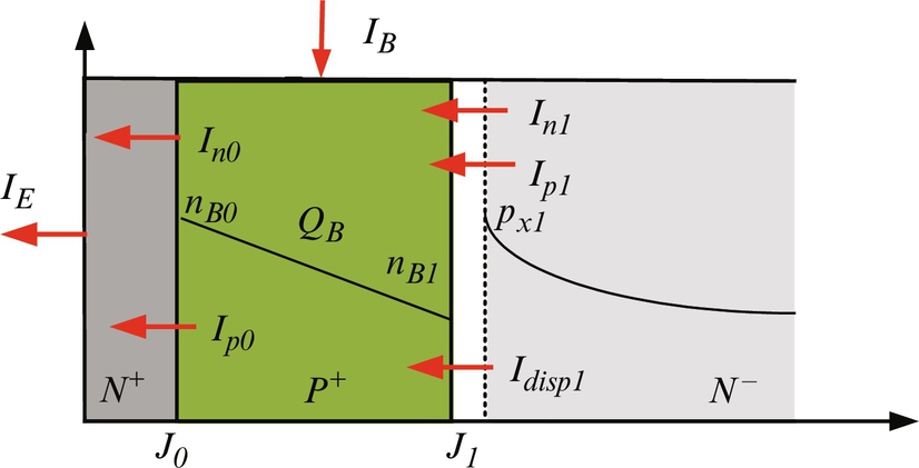
A basic one-dimensional structure of a power BJT is illustrated in Fig. 5.11. The BJT is divided into four regions: N+ emitter, P base, N− drift, and N+ collector. The external (emitter base and collector currents, IE, IB, and IC) and internal electron and hole and displacement currents (at junctions J0—In0, Ip0; J1—In1, Ip, and Idisp1; and J2—In2, Ip2, and Idisp2) are indicated for each region.
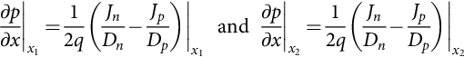
The N+ emitter layer of a power BJT can be simply characterized as a hole sink. The hole current at the junction, J0, is obtained by the following equation:
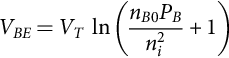
where nB0 is the electron concentration at junction J0 and PB is the base doping concentration. The N+ emitter recombination parameter, hn, depends on emitter properties, such as doping level (NE), hole diffusivity (Dp), and hole minority lifetime (τp). The electron current component at junction J0 is determined by
and the voltage drop across junction J0 is
The equation for the P-base region can be used to derive the boundary current at junction J1. The lumped-charge method is used to model the behavior in the base region due to its moderate doping level and comparatively narrow base width. The injected carrier distribution in the base region during conduction is shown in Fig. 5.12.
Using the continuity equation for the base region, the injected minority carrier charge is described by the relation:

where τBHL is the high-level lifetime in the P-base region.
The total electron charge in the base is expressed as
where WB is the base width. The electron concentration at the base region boundary on the collector side, nB1, is related to the excess carrier concentration, px1, by the doping concentration of the base, PB, by the equation:

Since the diffusion length in the base region is much greater than the base width, the gradient of the electron concentration is approximately linear, giving the electron current at the base-collector junction, J1, as
The base-emitter voltage VBE is calculated by the equation:
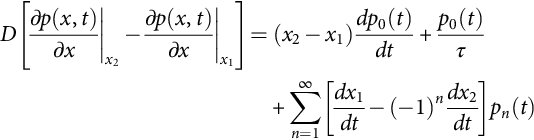
The voltage drop in N− drift region is calculated during the ON-state in a manner similar to that of a PiN diode. The injected excess carrier concentration is determined by the ADE. As for all power switches, high-level injection and quasineutral conditions exist. Under high-level injection conditions, the ADE for the lightly doped drift describes the carrier dynamics of the majority carriers:

where D is the ambipolar diffusion coefficient, τ is the high-level carrier lifetime within the drift region, and p(x, t) is the excess carrier concentration. The Fourier series solution of the ADE is given by the following first-order differential equations as each of them refers to a harmonic, pk(t), of the total minority carrier density, p(x,t):
For k>0

for ![]()
The solution to the ADE is determined by using the boundary conditions at the edges of the charge storage region. The representation requires the width of the undepleted region and the hole and electron currents at the boundaries of the drift region, which give the gradients of the carrier concentrations at x1 and x2, respectively. For the given direction of the currents (Fig. 5.13), the required boundary conditions are given by the equations:


Using the boundary condition Equation (5.112), the left side of Eq. (5.111), for even and odd numbers of k, can be calculated by the following equations:

The boundary carrier densities, px1 and px2, at the boundaries, x1 and x2, are calculated using the equations:

The voltages across the N−N+ and N−P+ depletion layers, Vd1 and Vd2, are calculated by the following equations:

The feedback constant, KFV, is set to 10−12, which gives good convergence and minimal error [68]. The associated depletion widths, Wd1 and Wd2, are calculated using a step doping concentration change on each side of the junction:

The boundary positions, x1 and x2, are calculated by
The displacement currents, Idisp1 and Idisp2, are due to the changing depletion widths at junctions J1 and J2:

The voltages across junctions J1 and J2 are

The voltage drop across the carrier storage region, ![]() , is calculated based on the injected carrier concentration discussed in Section 5.3.2.2.
, is calculated based on the injected carrier concentration discussed in Section 5.3.2.2.

where the carrier distribution, pT(k), is calculated as

The N+ collector region has similar properties to the N+ emitter region as it also can be presented as a hole sink. The hole current at junction J2 is obtained by the equation:
The electron current at junction J2 is
During the ON-state, the voltages across the N−N+ and N−P+ depletion layers, Vd1 and Vd2, are equal to zero, and the collector-emitter voltage is
Substituting the junctions' voltages from Eqs. (5.104), (5.120) in Eq. (5.125) and simplifying, the following equation will be obtained:

Since the thickness of the lightly doped drift region of a SiC BJT is smaller than the lightly doped drift region of a Si device, their boundary carrier densities, px1 and px2, at the boundaries, x1 and x2, are bigger [71]. Therefore, for the same doping concentration of the four regions of a power SiC BJT and a power Si BJT, the first term of Eq. (5.126) for a SiC device is big compared with a Si one. Also, if it is assumed that the intrinsic carrier concentrations of Si and SiC are 1010 and 10−10 cm−3 and the thermal voltage, VT=0.256, the second term of a Si device is a negative number (approximately −2.36 V) that will subtract from the first term and make collector-emitter voltage smaller, while for a SiC BJT, the second term is a positive number (~2.36 V) that will add to the first term and make the collector-emitter voltage bigger. Only the voltage drop in the lightly doped drift region for SiC will be small compared with a Si one, since the thickness in Si is significantly larger and the doping concentration in Si is lower. To have benefits of conductivity modulation and therefore small ON-resistance, SiC BJTs similar to SiC PiN diode should be designed for higher than 4 kV [112]. Also, the BJT is a bipolar device having minority and majority carrier flowing during operation; therefore, the drift region stores charge that decreases the device switching speed and thus can only operate at switching frequencies less than can be obtained with a MOSFET structure.
5.3.6 SiC IGBT
As previously mentioned, the rapid improvement in 4H-SiC material quality and the maturing of SiC device processing in recent years have enabled the development of high-voltage SiC power devices (MOSFETs and JFETs). However, the ON-resistance of SiC MOSFETs and JFETs rapidly increases as the blocking voltage and operating junction temperature increase because they are unipolar devices and conductivity modulation is not happening in the lightly doped drift region. This makes the conduction loss of the unipolar devices unacceptable for applications with a blocking voltage higher than 10 kV. For these applications, bipolar devices are preferred because they have been shown to have a small voltage drop due to strong conductivity modulation in their drift regions [113].
Simple gate drive interfaces make 4H-SiC IGBTs attractive devices. Chronologically, the first fabricated and characterized IGBTs were P-channel because there was a practical limitation in producing the low resistivity P+-type SiC substrate required for fabricating N-channel IGBTs [114]. But with the advantages of the SiC technology, N-channel IGBTs have been built. Both N- and P-channel SiC IGBTs have demonstrated high blocking voltage capability, as the first IGBT fabricated in 2006 had a blocking voltage of 5.8 kV. Since then, different IGBTs have been built; for example, 12 kV P-channel IGBTs with 14 mΩ cm2 ON-resistance [115], 13 kV N-channel IGBTs with 22 mΩ cm2 ON-resistance [116], and 20 kV self-aligned P-channel DMOS-IGBTs have been reported [117]. The 20 kV P-channel IGBT has a less than 15 times a smaller voltage drop at 31 A cm−2 current density compared with a theoretical MOSFET with the same blocking voltage [117]. The last reported IGBT with ultrahigh blocking voltage of 27 kV was reported in 2015 [118].
Different SiC device research groups have been working on optimizing the IGBT parameters and fabricating and characterizing devices so that soon IGBTs will be on the market. For a given blocking voltage, a trade-off between conduction and switching loses should be made to optimize the IGBT parameters. A reason for this is that there is a huge amount of charge stored in the IGBT lightly doped drift region during the ON-state and that has to be removed during turn-OFF [119].
In [120], the device group from Cree Inc. has fabricated a 10 kV MOSFET and an N-type IGBT capable of flowing 10 and 4 A, respectively. Both devices were processed identically through the device fabrication process each as a MOS part where the lightly doped drift region had the same length and doping concentration. The only difference between the two devices is that the N-channel IGBTs have a moderately doped N field-stop (FS) buffer layer and a heavily doped P+ injector, while the MOSFET has an N+ substrate. The DC characteristics of the devices were measured, and it was observed that the forward voltage drops of the two structures were the same, ~5 V.
The switching results indicated that both devices were much faster than the highest voltage, commercially available Si IGBT. The MOSFET turn-OFF transient time was faster than the IGBT turn-OFF time of 140 and 400 ns, respectively. A reason for slow turn-OFF time is that the IGBT is a bipolar device and stores minority and majority charges in the lightly doped drift region that are removed slowly, while the MOSFET is a unipolar device and is not dependent on carrier recombination during turn-OFF. The IGBT turn-OFF transient can be improved by reducing gate resistance and optimizing the internal capacitance and increasing the high-level lifetime.
Seven years later, the Cree Inc. group demonstrated a 20.7 kV N-channel IGBT with a forward voltage drop of 6.4 V at a collector current of 20 A and a 17 kV N-channel IGBT with a forward voltage drop of 5.7 V at a collector current of 20 A [121]. The two IGBTs were fabricated with the same mask sets and identical fabrication process. Although the lightly doped drift region for the 20.7 kV IGBT was significantly increased in width to support higher voltage, the voltage drop did not increase significantly, which can be attributed to conductivity modulation that takes place during the conduction state of the IGBT. Similar to a SiC PiN diode and a BJT, as an IGBT is a bipolar device, the junction voltage drops are dominant in determining the forward voltage drop with a blocking voltage smaller than 20 kV. The ON-resistance for an IGBT will be dominated by the parasitic resistance, such as channel resistance and the contact resistance, while the resistance of the lightly doped drift region will not be much larger due to high-level injection in the lightly doped drift region leading to conductivity modulation.
Results of a comparison of N-channel and P-channel SiC IGBTs have shown comparable static characteristics that can be explained by the fact that during the ON-state, an IGBT is operating at high-level injection. Regardless of the structure of an IGBT, the behavior of the carriers in the lightly doped drift region is governed by the ADE:
Operating at high-level injection means that the injected carriers in the lightly doped drift region have significantly higher values than the background impurity doping concentration. The electron and hole concentrations in the drift region during the ON-state are equal:
Their concentrations depend on the boundary conditions at each end of the drift region, the minority charge-carrier lifetime, and the drift region width. Assuming that N-channel and P-channel IGBTs are processed identically through the device fabrication process and the gate-source voltage and collector current are the same, then the carrier concentration in the drift region of the two devices will be equal, and therefore, the voltage drop across the drift regions will be the same. The IGBT junction voltages are functions of the doping concentrations, and they will be the same for the identically processed N- and P-channel IGBTs. Therefore, the total voltage drop for identically processed N-channel and P-channel SiC IGBTs will be significantly the same when the devices are subjected to the same conditions: gate-source voltage, collector current, and temperature.
On the other hand, N-channel IGBTs offer far superior switching characteristics over P-channel IGBTs. In Ref. [122], the simulation results of the switching characteristics of N-channel and P-channel 15 kV SiC IGBTs are given that support this fact. The rate of increase in the collector-emitter voltage of an N-channel IGBT is 40 V ns−1 and for a P-channel IGBT is 5 V ns−1. The current decay for the N-channel IGBT is also faster than the current decay for the P-channel IGBT. A physical explanation for this is that in the beginning of the turn-OFF process, the collector-emitter voltage, VCE, rises from the forward voltage, VF, to the DC supply voltage, VDC, and the rate of change of the VCE depends on the rate of removal of the stored charge through the emitter side. During this time, the recombination and displacement currents are significantly smaller than the minority carrier current and can be neglected. The minority current is responsible for the charge removal. As the VCE rises, the depletion region expands toward the collector junction. The minority carriers are swept out through the depletion region, and the majority of carriers are pushed toward the collector where most of them will recombine in the P+ injector layer for an N-channel IGBT or N+ injector layer for a P-channel IGBT [119]. Due to the large rate of change in the minority carrier current, the depletion region expends faster in an N-channel IGBT than in a P-channel IGBT, and therefore, the collector voltage for N-channel an IGBT rises at a faster rate. During the second phase of the turn-OFF process, after the collector-emitter voltage, VCE, reaches the DC supply voltage, VDC, the freewheeling diode is turned ON that allows the collector current to fall down to a value depending on the remaining storage charge. During this time, the VCE overshoots due to the energy stored in the stray inductance in the collector-emitter loop. After that, the collector current depends only on the remaining storage charge, and the recombination rate depends on the high-level carrier lifetime [123]. Since the holes' lifetime is smaller than the electrons' lifetime, the tailing current phase is shorter for an N-channel IGBT compared with a P-channel IGBT. Also, an N-channel IGBT has faster charge extraction due to the large ionization energy of acceptors in 4H-SiC [122]. Since the total losses for an N-channel IGBT are smaller compared with a P-channel IGBT, further developments in IGBT should be focused on an N-channel IGBT [118].
Similar to other power devices, IGBTs consist a thick lightly doped drift region that is required to support high voltage and prevent an avalanche breakdown. The drift region thickness, the doping concentration, and the minority carrier lifetime are important IGBT design parameters. Their values are optimized so that the sum of the conduction and switching losses is minimized for a desired blocking voltage. The drift region thickness and doping concentration are optimized to obtain minimum conduction loses (forward voltage drop) for the same blocking voltage. Increasing the doping concentration requires a thicker drift region to sustain the high voltage and prevent an avalanche breakdown. The minority lifetime effects the conducting and switching losses. An increase in the lifetime enhances the conductivity modulation, and therefore, the forward voltage drop is reduced, while the recombination process becomes slower and results in high switching losses. A compromise between conduction and switching losses should be made to optimize the carrier lifetime in the drift region.
To decrease the drift region thickness for the same IGBT blocking voltage, an FS layer adjacent to the lightly doped drift region is used, making the IGBT an asymmetrical device. In [124], it is shown that a 15 kV N-channel symmetrical IGBT does not have an FS layer and the thickness of the drift region is 247 μm, while for an asymmetrical N-channel IGBT, the thickness is 150 μm. Therefore, the voltage drop in the lightly doped drift region is significantly smaller for an asymmetrical device. Also, due to the FS layer, the depletion width starts to expand across the whole drift region when an IGBT is switched OFF and a punch-through effect is observed. Therefore, the depletion width that is equal to the drift region thickness should be designed first. The punch-through effect benefits the switching characteristics of an IGBT. After the punch-through, the sweep-out of the excess carriers practically stops, and the charge removal is performed mostly due to the recombination process in the FS layer. Therefore, the current tail disappears under the punch-through condition. The punch-through effect has some disadvantages also. During punch-through, the parasitic capacitance associated with increasing of the VCE turns into a much smaller capacitance instead of a large diffusion capacitance [121]. This capacitance resonates with the parasitic stray inductance in the collector-emitter loop resulting in voltage overshooting and a ringing phenomenon, which should be carefully considered. The thickness of the FS layer is an important device parameter. Increasing the FS layer thickness results in superior turn-OFF speed but slightly increases the forward voltage drop, while decreasing the FS layer thickness slows down the turn-OFF speed but offers superior conduction capability [125].
To reduce the ON-state resistance of the lightly doped drift region of an N-channel IGBT, some power device designers have inserted a thin, heavily doped N+ current spreading layer (CSL) beneath the P-type base region, forming a JFET layer between the two P bases. An CSL helps to distribute the electron flow more uniformly, minimizing the current crowding at the top of the drift region and reducing the drift layer resistance. Both regions, CSL and JFET, are formed as N-type epitaxial layers having higher doping concentration than the drift layer. Increasing the doping concentration in the JFET region helps to reduce the ON-state resistance; however, it causes an increase in the electric field at the SiC-SiO2 interface during the blocking state. Simulation results have shown that for a drift region width higher than 1.6 μm, the oxide field reaches 4 MV cm−1 prior to the avalanche breakdown in SiC. Decreasing the JFET width increases the resistance since it pinches off the current path but reduces the cell area; consequently, the effect of the specific ON-resistance is negligible [77]. An optimum width of the JFET region can be determined. When an IGBT has an optimum width, its blocking voltage is limited by the avalanche breakdown for the entire range of the lightly doped drift region. In [126], it is shown that for their design, the optimum width is 1 μm.
To optimize the parameters of a PT IGBT, a physics-based model, given in [127], can be used. For this purpose, the device is divided into five regions, as shown in Fig. 5.14: P emitter (collector terminal), N+ field-stop layer, N− drift region, P well, and N+ emitter. Fig. 5.14 also shows the external currents (emitter and collector currents IE and IC), the internal electron and hole currents (at junctions J0 In0 and Ip0, J1 ![]() and
and ![]() , and J2
, and J2 ![]() and
and ![]() ), and the capacitive currents from the displacement layers (
), and the capacitive currents from the displacement layers (![]() and ICG). The IGBT is a gate-controlled device and is used as a controllable switch in power electronic applications. Given its P-N-P-N structure, the IGBT is a voltage bidirectional switch, that is, it can conduct current in one direction only, but it can block the voltage of both polarities. The reverse-blocking capability is rarely used in conventional power converter configurations. Frequently, an antiparallel diode is added as a separate chip to accommodate converter configurations, such as the voltage source inverter, which require a current bidirectional switch. In the normal forward blocking operation of the IGBT, a depletion layer is formed at the MOS end of the drift region (at the N− drift region/P-well junction), while in a reverse-blocking operation, it is formed at the P emitter/drift region junction. In forward blocking, a depletion layer is never formed at the P emitter. For this reason, no displacement current for junction J0 is included. The model can be easily extended to reverse-blocking IGBTs by allowing a depletion layer at the junction J0.
and ICG). The IGBT is a gate-controlled device and is used as a controllable switch in power electronic applications. Given its P-N-P-N structure, the IGBT is a voltage bidirectional switch, that is, it can conduct current in one direction only, but it can block the voltage of both polarities. The reverse-blocking capability is rarely used in conventional power converter configurations. Frequently, an antiparallel diode is added as a separate chip to accommodate converter configurations, such as the voltage source inverter, which require a current bidirectional switch. In the normal forward blocking operation of the IGBT, a depletion layer is formed at the MOS end of the drift region (at the N− drift region/P-well junction), while in a reverse-blocking operation, it is formed at the P emitter/drift region junction. In forward blocking, a depletion layer is never formed at the P emitter. For this reason, no displacement current for junction J0 is included. The model can be easily extended to reverse-blocking IGBTs by allowing a depletion layer at the junction J0.

The hole and electron currents in the P-emitter layer end of a power IGBT at junctions, J0, Ip0, and In0, depend on the process happening in the FS layer. The sum of them is equal to the IGBT collector current:
where NN is the doping concentration of the FS layer.
Adding an FS layer allows a reduction in the drift region thickness for the same blocking voltage and also speeds up the IGBT turn-off process but creates two junctions, J0 and J1. Due to electron reverse injection into the P+ emitter, there is a small electron current In0 at junction J0. These electrons travel through the buffer layer from the drift region. The hole current, Ip0, injected from the P+ emitter, travels mostly by diffusion through the FS layer. Since the layer is typically quite thin in comparison with the hole diffusion length, ![]() , there is little recombination, and most of the holes reach the drift region. This hole current is Ip1 and represents the hole injection from the buffer layer into the drift region.
, there is little recombination, and most of the holes reach the drift region. This hole current is Ip1 and represents the hole injection from the buffer layer into the drift region.
The difference between the two hole currents at junctions J1 and J0 is due to the recombination, and it is compensated for by an increase in the electron current, so that the electron current In1 at junction J1 can be presented by a sum of the recombination component plus the reverse injection electron current In0. Static conditions are assumed up to now, while under dynamic conditions, an additional hole current component due to variations in the stored charge in the buffer layer should be considered.
Assuming a quasistatic state, the continuity equation of the holes in the buffer layer is then expressed by
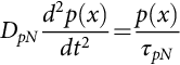
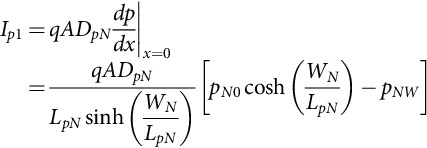
where τpN is the minority lifetime and DpN is the hole diffusivity in the field-stop layer. The solution for the excess hole concentration in the buffer layer is given by
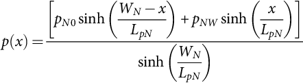
where WN is the width of the buffer layer, pN0 and pNW are the hole concentrations at the two edges of the field-stop layer (junctions J0 and J1), and LpN is the hole diffusion length.
Under the low-level injection, the minority hole current is mostly diffusion current, so it is expressed as

Thus, the hole current at the junction J0 is obtained substituting the derivative of Eq. (5.131) for ![]() into Eq. (5.132):
into Eq. (5.132):

Assuming quasiequilibrium, the reverse injection current In0 at junction J0 is given by
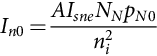
where Isne is the emitter electron saturation current.
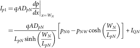
The current continuity at the boundaries of the buffer layer requires that
Then, the hole concentration at the junction J1 is obtained by substituting Eqs. (5.133), (5.134) into Eq. (5.135) and then reorganizing the equation to the form:

The hole current Ip1 at junction J1 is obtained similar to Ip0, only ![]() :
:
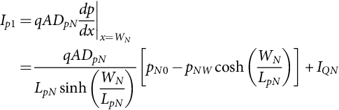
The current, IQN, represents the capacitive current due to the variation in the charge QN stored in the buffer region:

The charge QN can be approximated as
The hole concentration, pNW, at the boundary between the buffer layer and the drift region is obtained by applying the Boltzmann relationship for the junction J2 under the assumption of high-level injection in the drift region (![]() ):
):
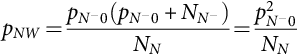
where ![]() is the hole concentration in the beginning and
is the hole concentration in the beginning and ![]() is the doping concentration of the N− drift region.
is the doping concentration of the N− drift region.
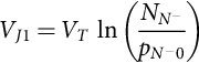
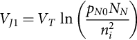
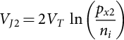
The voltages across the junctions J0 and J1 are

The voltage drop in the N− drift region is calculated during the ON-state. The charge distribution and the boundary current components in the N− region are shown in Fig. 5.15. The injected excess carrier concentration is determined by the ADE. As for all bipolar power switches, high-level injection and quasineutral conditions exist. Under high-level injection conditions, the ADE (Eq. 5.35) describes the carrier dynamics.

It was mentioned that, during forward blocking of an IGBT, no depletion layer forms at junction J1; therefore, its thickness, x1, can be approximated as zero. Therefore, the charge storage region, which operates under high-level injection and is described by the ADE, Eq. (5.35), has ![]() and
and ![]() . The Fourier series solution of the ADE, given by Eq. (5.39), can be simplified to
. The Fourier series solution of the ADE, given by Eq. (5.39), can be simplified to
For ![]()

For ![]()

The solution to the ADE is determined by using the boundary conditions at the edges of the charge storage region:
The current continuity equation at junction J2 is determined by
The electron current at junction J2 is the MOS channel current:
Substituting Eqs. (5.146) in (5.145) and then in Eq. (5.143), the left side of the solution of the ADE (Eq. 5.143), for even and odd numbers of k, can be calculated by the following equations:

The boundary carrier densities px1 and px2 at the boundaries x1 and x2 are calculated using the equations:

The voltage across the N−P depletion layer, ![]() , is calculated by the following equation:
, is calculated by the following equation:

The associated depletion width, ![]() , is calculated using a step doping concentration change on each side of the junction:
, is calculated using a step doping concentration change on each side of the junction:

The boundary position x2 is calculated by
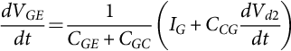
The displacement current at x2 is composed of two components: ![]() flowing into the P well and ICG associated with Miller capacitance and accumulation layer charge. The P-well displacement current is given by
flowing into the P well and ICG associated with Miller capacitance and accumulation layer charge. The P-well displacement current is given by

To calculate the Miller capacitance, it is assumed that the depletion layer extends under the gate from P well and only extends downward through the drift region once the accumulation layer has been removed from the gate in the center of the intercell region. Therefore, the width of the Miller capacitance, W, is
where lm is an intercell half width and l1 is a width due to voltage VGE:

The Miller capacitance is given by the series combination of the oxide capacitance CoxAai and the depletion capacitance ![]() :
:
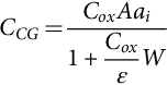
where ai is the ratio of intercell area to the total die area.
Due to Miller capacitance, the current ICG is
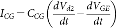
where
The voltage drop in the carrier storage region ![]() is calculated based on the injected carrier concentration:
is calculated based on the injected carrier concentration:

where the carrier distribution pT(k) is calculated as
IGBTs are used as switches, operating mainly in two stages: ON and OFF. The MOS region can be modeled as a simple MOSFET. During the ON-state, the MOSFET operates either in the triode region or in the saturation region, while during the OFF-state, it operates in cut-OFF. Therefore, during the OFF-state, the gate-source voltage is smaller than the threshold voltage ![]() , and current Imos is zero. During the ON-state, the gate-source voltage is larger than the threshold voltage
, and current Imos is zero. During the ON-state, the gate-source voltage is larger than the threshold voltage ![]() , and current Imos is calculated by
, and current Imos is calculated by

The voltage drop VCE across PT IGBT is composed of three components: voltages across the junction J1, voltage across the two depletion regions Vd2, and voltage across the carrier storage region ![]() .
.
5.3.7 SiC Thyristor
As the trend of power electronics industry is moving toward high voltage, high current, and high frequency, the conduction and switching losses of the power semiconductor devices should be at an acceptable level. Up to now, SCRs are still the most powerful devices currently available in pulse power applications. A single SCR can block 8 kV and conduct 4 kA, and a GTO can block 6 kV and conduct 6 kA [128]. However, due to the high switching losses of SCRs and GTOs, their maximum operation frequency is limited to 1 kHz. Because of their switching and driving characteristics, the device paralleling for high-power applications is impossible. SCRs and Si GTOs have a positive temperature coefficient and their operating temperature is limited to 100°C junction temperature, since the leakage current increases significantly above that temperature. Typically, this requires expensive active liquid cooling to maintain safe operation conditions. The leakage current of a SiC GTO is extremely small at 300°C and only requires forced air cooling.
SiC GTOs and IGBTs are two devices that can soon be utilized in utility-based power handling equipment, such as flexible AC transmission systems (FACTS) and high-voltage DC transmissions (HVDCT). A 4H-SiC thyristor is a better candidate because it is capable of higher current densities than a SiC IGBT, since the physical mechanism for conductivity modulation is more effective in the thyristor than the IGBT. Also, SiC IGBTs are limited to 150°C junction temperature due to a limitation of the gate oxide reliability.
In the near future, large-area SiC GTOs will be utilized in FACTS and HVDCT due to three main advantages: a smaller number of devices connected in series since they have higher blocking capability (20–30 kV with the present technology), low current leakage, and reduced cooling requirements due to the ability of SiC GTOs to operate at higher junction temperatures (300°C if the packaging issues are solved). However, the thyristor requires more complex external circuitry as it is a current-controlled device.
The first SiC symmetrical thyristors (700 V with a rated current of 6 A and a forward drop of 3.9 V) were demonstrated by Cree, Inc. [129]. Since then, scientists from Cree and other institutions have designed and fabricated different asymmetrical NPNP devices. The limitations of the epilayer thickness and device footprint have been the main obstacles for increasing the blocking voltage and the current capability of the devices, but different scientific groups have worked in the last two decades to improve design, fabrication, and characterization of different power semiconductor devices that were used for an evaluation of SiC GTOs from 1.77 kV blocking voltage with 4 V voltage drop at 100 A and 200°C [130] demonstrated in 2005 to a 22 kV blocking voltage with approximately 6.5 V voltage drop at 100 A and 150°C reported 10 years later. The most important developments of this evaluation were increasing the wafer diameter to 5.9′′ (150 mm) [131]; the electrically active defects, such as dislocations, point defects, and silicon inclusion, have been drastically reduced; the problem of the foreword voltage drop, VF, drift due to high density of the basal plane dislocation has been solved by improving the epitaxial growth; and improving the life time of the minority carrier concentration in the lightly doped drift region.
Due to very high blocking voltage (>20 kV) for SiC GTOs, they have a low-doped thick drift region that has high resistivity. In order to obtain significantly low ON-state losses, the ambipolar diffusion length of the minority carriers in the drift region should be significantly large, that is, the minority carrier lifetime must be made as long as possible. For an N-type SiC epilayer, a significant improvement of carrier lifetime has been achieved from 0.69 to 9.5 μs by reducing the Z1/2 center via two-step thermal treatment (thermal oxidation and Ar annealing) for a 148 μm N-type epilayer [132]. However, there is some difficulty for enhancement of the carrier lifetimes in p-type epilayers [133]. In [134], the lifetime in P-type SiC epilayer was improved from 1 to 4 μs by oxidation at 1300°C for 5 h prior to the metal contact processing; however, the carrier lifetime was not uniform across the chip area. The lifetime uniformity can be enhanced by controlling the point defects in SiC by low-energy electron irradiation [132].
Currently, the thyristors are made on N+ 4H-SiC substrates, because P+ substrates have higher resistance than the N+ substrates. Recently, a significant improvement in N+ 4H-SiC substrate quality has been reported. An IGBT with an ultrahigh blocking voltage of 27 kV was built on N+ 4H-SiC substrate [118]. For a Si power thyristor to minimize power losses, the epilayer is N− type. Therefore, in the future, power thyristors will build on P+ substrate with an N− epilayer.
To optimize the parameters of the transistor, a physics-based model for GTOs employing a Fourier-based solution for the ambipolar diffusion equation of the N− lightly doped drift region and a lumped-charge method for the P-base region can be used. A new level-3 physics-based model for GTOs employs a Fourier-based solution for the ambipolar diffusion equation of the lightly doped N− drift region, and a lumped-charge method for the P-base region is provided below. In addition to the external electric characteristics, the model can also provide internal physical and electric information, such as junction voltages, and the charge distribution in the buffer layer and the base regions. Fig. 5.16 shows the schematic structure of a SiC high-power thyristor with the direction of the flowing currents.
A major difficulty in analyzing and modeling the performance of bipolar power devices is due to the different carrier density distribution in the different regions. The behavior of the GTO is modeled by dividing the device into different regions.
The P+ and N+ emitter regions have high doping concentration, and therefore, there is a significant electron concentration adjacent to the P+N junction and a significant hole concentration adjacent to the PN+ junction due to the equal concentrations of holes and electrons. As a result of these high concentrations, minority carriers flow into the highly doped P+ and N+ emitter regions, where they recombine with holes and electrons, respectively. The process is known as emitter recombination. The resulting electron and hole currents due to the recombination are
where pN0 and nPW are the hole and the electron concentrations at junctions J0 and J3, respectively. The recombination parameters, hp and hn, calculated by Eqs. (5.32), (5.63), depend on the emitter properties, such as doping level (![]() and
and ![]() ), electron and hole diffusivities (Dn and Dp), and electron and hole lifetime (τn and τp). The hole and emitter currents in the P+ and N+ emitter regions are
), electron and hole diffusivities (Dn and Dp), and electron and hole lifetime (τn and τp). The hole and emitter currents in the P+ and N+ emitter regions are
Adding a buffer layer allows a reduction of the drift region thickness for the same blocking voltage and speeds up the thyristor turn-off process, but it creates two junctions, J1 and J2. Due to electron reverse injection into the P+ emitter, there is a small electron current, In0, at junction J0. These electrons travel through the buffer layer coming from the drift region. The hole current, Ip0, injected from the P+ emitter travels mostly by diffusion through the buffer layer. Since the buffer layer is typically quite thin in comparison with the diffusion length in the buffer layer, ![]() , there is little recombination in the buffer layer, and most of the hole current reaches the drift region. This current, Ip1, presents the hole injection from the buffer layer into the drift region.
, there is little recombination in the buffer layer, and most of the hole current reaches the drift region. This current, Ip1, presents the hole injection from the buffer layer into the drift region.
The difference between the two hole currents at the junction J1 and J0 is due to the recombination, and it is compensated by an increase in the electron current, so that the electron current In1 at junction J1 can be presented by a sum of the recombination component plus the reverse injection electron current In0. Static conditions are assumed up to now, while under the dynamic condition an additional hole current component due to variations in the stored charge in the buffer layer should be consider.
Assuming a quasistatic state, the continuity equation of the holes in the buffer layer is then expressed by
where τpN is the minority lifetime and DpN is the hole diffusivity in the buffer layer. The solution for the excess hole concentration in the buffer layer is given by
where WN is the width of the buffer layer, pN0 and pNW are the hole concentrations at the two edges of the buffer layer (junctions J0 and J1), and LpN is the diffusion length of the holes.
Under the low-level injection, the minority hole current is mostly diffusion current, so it is expressed as

Thus, the hole current at the junction J0 is obtained by substituting the derivative of Eq. (5.167) for ![]() into Eq. (5.168):
into Eq. (5.168):
Assuming quasiequilibrium, the reverse injection current In0, at junction J0 is given by

where Isne is the emitter electron saturation current, which is usually small, and NN is the doping concentration of the buffer layer.
The current continuity at the boundaries of the buffer layer requires that
Then, the hole concentration at the junction J1 is obtained by substituting Eqs. (5.169), (5.170) into Eq. (5.171) and then reorganizing to the form:

The hole current, Ip1, at junction J1 is obtained similar to Ip0, only ![]() :
:
The current, IQN, represents the capacitive current due to the variation in the charge, QN, stored in the buffer region.
The charge, QN, can be approximated as
The hole concentration, pNW, at the boundary between the buffer layer and the drift region, is obtained by applying the Boltzmann relationship for the junction J1 under the assumption of high-level injection in the drift region ![]() :
:

where ![]() is the hole concentration in the beginning and
is the hole concentration in the beginning and ![]() is the doping concentration of the N− drift region that is denoted below as px1.
is the doping concentration of the N− drift region that is denoted below as px1.
The voltages across the junctions, J0 and J1, are

The GTO thyristor requires a thick drift region to support a high blocking voltage. A simple charge control modeling approach cannot be applied for the drift region because the transient duration compares with or is shorter than the transient time of the charge carriers. In this case, the charge dynamics in the drift region can be described by the continuity and the transport equations. The charge profile in the thick drift region can be assumed as one-dimensional over more than 90% of the volume, which makes the analysis simple. Also, high-level injection conditions can be assumed during the time of the transient and static state. Under this assumption and quasineutrality, the one-dimensional ambipolar diffusion equation that describes the carrier dynamics in the majority of this region is given by Eq. (5.35). The equations from Section 5.3.2.2 for SiC PiN diodes in Eqs. (5.35)–(5.61) are the same for a power GTO, so it will not be repeated.
The junction voltage VJ2 between the lightly doped drift region N− and the P base is
The lumped-charge method can be used to model the charge behavior in the base region due to high doping level and comparatively narrow base width. Using the continuity equation for the base region, the injected minority carrier charge can be described by the relation below:
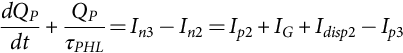
where τPHL is the high-level lifetime in the P-base region. The electron concentration at the P-base region boundary, nP0, is related to px2 by the doping concentration of the base, NP, by the equation:

The total electron charge in the base can be expressed as
where nPW is the electron concentration at the base region boundary from the N+ emitter side and WP is the base width. Since the diffusion length in the P-base region is much greater than the base width, the gradient of the electron concentration may be approximated linearly. Then, the electron current at junction, J3, is
The junction voltage VJ3 between the P-base and the N+ emitter can be calculated by the equation:

The voltage drop VAK across the SiC thyristor is composed of seven components including voltages across junctions J0, J1, J2, and J3, the voltage across the two depletion regions, Vd1 and Vd2, and the voltage across the drift region, ![]() :
:
5.4 GaN Power Devices
Due to the significant improvements in GaN material growth technology, engineers have utilized different GaN-based power devices in high-frequency and power applications. The device designers are trying to improve performance and reliability and optimize their FOM parameters to obtain high system efficiency. GaN HEMT devices ranging up to 650 V are available on the market. The physics and important parameters of GaN power devices are discussed below.
5.4.1 Lateral GaN Schottky Barrier Diodes
To achieve a high-efficiency, high-density power conversion system, the high-voltage diodes used in a system should have low turn-ON voltage, VT, low ON-resistance, RON, low leakage current, and short reverse recovery time. Due to the wide bandgap of GaN and high electron mobility in the 2DEG, AlGaN-/GaN-based lateral Schottky barrier diodes (SBDs) on a Si, sapphire, or SiC substrate have demonstrated superior performance over rectifiers made in other material systems, such as gallium arsenide (GaAs)-based devices. The advantages of lateral GaN-based devices are that they have a very low ON-resistance because of the extremely high electron concentrations in the 2DEG, up to 10–20 times higher that GaAs-based devices. Lateral SBDs have a small junction capacitance compared with conventional Schottky diodes and, therefore, low reverse recovery times. Also, a lateral design approach enables the standard GaN HEMT process flow to be used for integrating a Schottky diode with a high-voltage transistor [135].
A cross section of a typical lateral AlGaN/GaN heterostructure Schottky diode is shown in Fig. 5.17. The epitaxial layers are grown by metal-organic chemical vapor deposition on a substrate, and then, two types of contacts, ohmic and Schottky, are formed.
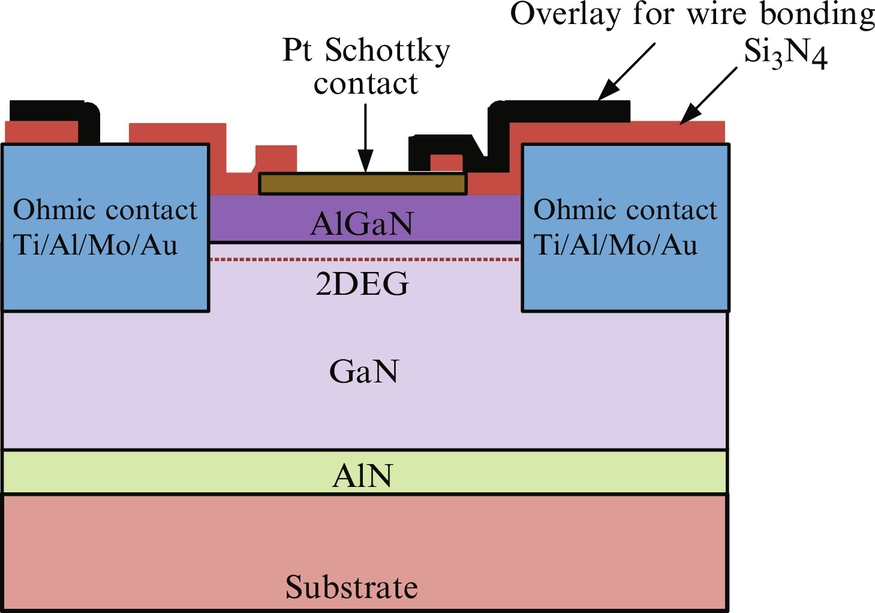
The quality of the epitaxial GaN depends on the quality of the substrate. Si, sapphire, SiC, and GaN can be used for the substrate. Si substrates have good quality, are significantly large in size, and are inexpensive. They can be used for GaN devices for low-power-density applications, where the losses are not high and the device temperature does not exceed the maximum operating junction temperature. Using a Si substrate for GaN devices introduces a number of critical issues due to the lattice mismatch and the difference in the thermal expansion coefficients, which affects the quality and device reliability [34]. Sapphire substrates are cost-effective and widely used for electronic devices with high power density and high-pulsed-output power densities, but it has a high lattice mismatch to GaN and poor thermal conductivity. Therefore, it is difficult to remove heat produced during operation. For high-power-density applications, the GaN devices should be grown on a SiC substrate since the SiC thermal conductivity is three times higher than Si, which leads to improved heat dissipation. The qualities of SiC substrates have improved significantly in the last few years, but they are still not widely available at low cost. GaN substrates have only recently been developed and used for power devices, although they are most important for optical applications. By using GaN substrates, the lattice mismatch is fully eliminated, but the cost of these substrates is high, and large diameters are not available. GaN layers grown on GaN substrates have low defect densities compared with layers grown on other types of substrate. Therefore, for devices of the same physical dimensions, devices utilizing GaN substrates will exhibit better OFF-state and ON-state characteristics.
Growth of GaN onto a Si or a sapphire substrate offers the very attractive potential for incorporating GaN devices. However, because of the large difference in lattice constant, crystal structure, and thermal expansion coefficient, it is difficult to epitaxially grow GaN. To solve this problem, a buffer layer that minimizes the mismatch between the substrate and GaN allows growth with a quality equal to GaN. Several buffer layer types have been used to grow GaN on Si, for example, SiC [136], AlN [137], GaAs [138] and silicon nitride (Si3N4) [139]. An AlN buffer layer is one of the best candidates for obtaining high-quality GaN on a Si substrate. It was found in [140] that a thicker AlN buffer layer resulted in higher crystalline quality of consequently grown GaN film.
The heterostructure consisting of undoped GaN and undoped zinc blende (cubic) (Al0.3Ga0.7N) is grown on the AlN buffer layer. Due to spontaneous and piezoelectric polarization, a 2DEG is created in the channel at the AlGaN/GaN interface [141]. The sheet electron density and the mobility in the channel are significantly high, ~1013 cm−2 and 1500 cm2(V s)−1, respectively, which result in low ON-state resistance.
Two types of contacts are formed in a lateral SBD. Metals or alloys such as palladium (Pd), platinum (Pt), indium-platinum (IrPt), palladium-silver (PdAg), and nickel/gold (Ni/Au) that have higher work functions than GaN can be used to form a Schottky barrier to the channel. The Schottky barrier is formed to the AlGaN interfacial layer of an AlGaN/GaN heterostructure. Since the channel has a high electron concentration, the depletion length is significantly shorter than in conventional diodes, although the lateral SBDs have a greater barrier height.
The ohmic contacts of a GaN power device (diodes and transistors), in most cases, represent a metal stack that is formed by thermal evaporation of different metals in multilayers following by rapid thermal annealing. The devices should be optimized to have low specific conduction resistance, and they should also be thermally stable. For N-type GaN, metal stacks such as titanium/aluminum/molybdenum/gold (Ti/Al/Mo/Au) and titanium/aluminum/platinum/gold (Ti/Al/Pt/Au) can be used to form ohmic contacts because of their excellent characteristics. A specific contact resistivity as low as 4.7×10⁻⁷ Ω cm−2 was obtained by rapid thermal annealing of evaporated Ti/Al/Mo/Au [142]. Also, Ti/Al/Pt/Au contacts on GaN have shown a minimum contact resistivity of 8.4×10⁻⁵ Ω?cm−2 after annealing [143].
Applying a positive bias, higher than the turn-ON voltage, VT, to the anode, causes electrons to flow from cathode to the anode. For an applied anode to cathode voltage, VAC, higher than 3kT/q, the current through the diode is

where A is the Schottky contact area and A⁎ is the Richardson constant (26.4 A cm−2K−2), and the potential barrier at the metal-semiconductor interface, ϕB, depends on the work function of the metal or alloy used for the Schottky contact.
As a negative bias is applied to the Schottky contact, a depletion layer between the Schottky contact and the 2DEG is formed. Increasing the negative voltage, the depletion layer expands and the junction capacitance decreases, resulting in a nonlinear capacitance-voltage characteristic [144]. A simple equivalent circuit model of a Schottky/2DEG diode is shown in Fig. 5.18. It consist of a voltage-dependent junction capacitance, Cj, series resistance, Rs, and a shunt capacitance, Csh, [144].

The junction capacitance, Cj, is
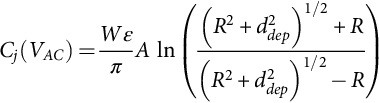
where W is the Schottky contact width and R is the half height of the Schottky metallization. The depletion width ddep is

where Vbi is the built-in voltage, VAC is the reverse bias applied voltage, and ns is the 2DEG sheet charge density. The series resistance, Rs, is a sum of the undepleted channel resistance, RCH, and the ohmic contact resistance, ROC:
The undepleted channel resistance, RCH, is
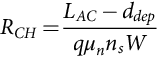
where LAC is the distance between anode and cathode (channel length) and μn is the electron mobility in 2DEG. The ohmic contact resistance, ROC, is
where rsp is the specific contact resistivity. The shunt capacitance, Csh, includes the ohmic contact (pad-to-pad) capacitance and Schottky contact-to-ohmic pad capacitance.
For high-voltage SBDs, the device channels are significantly long. Therefore, it can be assumed that the junction breakdown is caused either by impact ionization or by tunneling. The channel length, LAC, is a very important device parameter for a lateral SBD. By increasing the distance, LAC, larger breakdown voltages can be obtained, but the ON-resistance and, therefore, the conduction losses will be higher.
Different technologies have been studied to improve SBD performance. One of them uses an anode composed of two metals with different work functions. In this case, two types of contacts are formed: a Schottky and an ohmic, as shown in Fig. 5.19.

The low work function metal reduces the turn-ON voltage, VT, and the high work function metal at the edge of the anode reduces the reverse leakage current and maintains the breakdown voltage. In [145], it is shown that the turn-ON voltage of the SBD is reduced from 1.47 to 0.57 V by employing the dual metal anode, and the breakdown voltages are virtually unaffected.
Another technology that can be used to reduce the turn-on voltage, VT, without an increase in the leakage current is recess etching in the anode region of an SBD. The etching process must be well controlled because uneven etched surface morphologies can result in an increase in the surface leakage current [146]. A combination of an ohmic anode and a recessed Schottky gate, as shown in Fig. 5.19, is responsible for the low turn-ON voltage and an increase in the forward current. No breakdown-voltage degradation has been observed. In comparison with a conventional SBD, the forward current at 1.5 V is increased by two to three times in the SBD with a recessed dual anode metal, resulting in a breakdown voltage of 1440 V. The reason for this is that when a small positive voltage is applied to the anode, electrons flow from the cathode to the anode ohmic metal. Increasing the anode voltage so that the Schottky contact under the recessed anode region is turned on causes electrons to also flow through the Schottky metal. Additional electrons passing through the anode ohmic contact lead to very low turn-ON voltage, VT, and high forward current.
The recess depth, d, is an important design parameter for a Schottky GaN device. For devices with a higher value than the optimum recessed depth, the electrons tend to flow through the Schottky metal instead of through the anode ohmic metal so that the electrons flowing to the anode ohmic metal are suppressed. The blocking voltage is not affected by the recess depth. In [146], it is reported that an AlGaN/GaN on Si SBD with dual metal and 16 nm recess depth with 0.34 V turn-ON voltage, VT, has an anode current, IA, (at 1.5 V) equal to 1.63 A. A SBD with a maximum breakdown voltage of 1.9 kV was reported by [147].
Researchers have reaped the benefits of GaN lateral Schottky diodes, such as low turn-ON voltage, VT; low ON-resistance, RON; low leakage current; and low reverse recovery times. Improvements in the reliability of the GaN lateral Schottky diodes will make them the best candidates for high-power applications.
5.4.2 Vertical GaN PiN Diodes
GaN vertical devices have been studied extensively because of their potential to sustain high breakdown voltage without enlarging the chip area [148] and hence increasing the number of dies on a wafer. Also, vertical GaN devices have the potential to achieve a higher power at high temperature (150°C) than the lateral devices, especially for higher breakdown voltages and higher scaling level designs [149]. Vertical devices have high current capability and do not suffer from the thermal management issues associated with thin-film surfaces [150].
The reliability and performance of GaN-based devices depends on the defect density. GaN layers grown on foreign substrates (e.g., Si or SiC) create difficulties for realizing vertical devices because of higher defect densities (>108–109 cm−2) created. For fabricating devices with high breakdown-voltage capability, low leakage current, and high reliability, it is very important that the epitaxial layers have a low defect density. GaN layers grown on a GaN bulk substrate have significantly low defect densities (<106 cm−2), but the bulk GaN substrates are too expensive and currently have small diameters, which are the main challenges for the commercialization of the GaN vertical devices, although they have shown high performance. Scientists from different universities and companies are conducting ongoing research into improving the quality and increasing the size of the GaN substrates. The research is mostly driven by the optoelectronics industry in two directions: scalability and price reduction. Since there are already multiple suppliers of bulk GaN substrates, the development of GaN vertical power devices will increase soon.
In Fig. 5.20, a cross section of a vertical GaN PiN diode is shown. Similar to Si and SiC PiN diodes, a GaN PiN diode consists of a heavily doped N+ region, a lightly doped drift region, and a heavily doped P+ region. When a GaN vertical diode is built on GaN substrate, the substrate has a high electron concentration (1.5–2×1018 cm−3) and plays a role as a heavily doped N+ region. Some researchers have built a GaN vertical diode on a Si substrate. In this case, due to the lattice mismatch and differences in the thermal expansion coefficients between Si and GaN, a buffer layer of AlN/GaN or AlGaN is grown between the substrate and the epitaxial layer. The buffer layer improves the quality of the epitaxial layer grown on top of it. Then, a heavily Si-doped N-GaN layer (2×1018 cm−3) is grown.

As mentioned earlier for N-type GaN, metal stacks, such as Ti/Al/Mo/Au, Ti/Al/Pt/Au, and others, can be used to form low-resistivity stable ohmic contacts because of their excellent characteristics. Obtaining stable contacts with low resistivity for P-type GaN is more difficult due to the wide bandgap of GaN. Since the work function of P-type semiconductors is larger and for a wide bandgap it will be pronounced, a metal with a larger work function [151] is required to align the metal and semiconductor Fermi levels. Metal stacks, such as Ni/Au, Pd/Au, Ni/Pd/Au, and others, can be used for these ohmic contacts. An alloy of Ni/Pd/Au is reported to have good ohmic contact with a low specific resistance of 4.5×10⁻⁶ Ω cm2 [152].
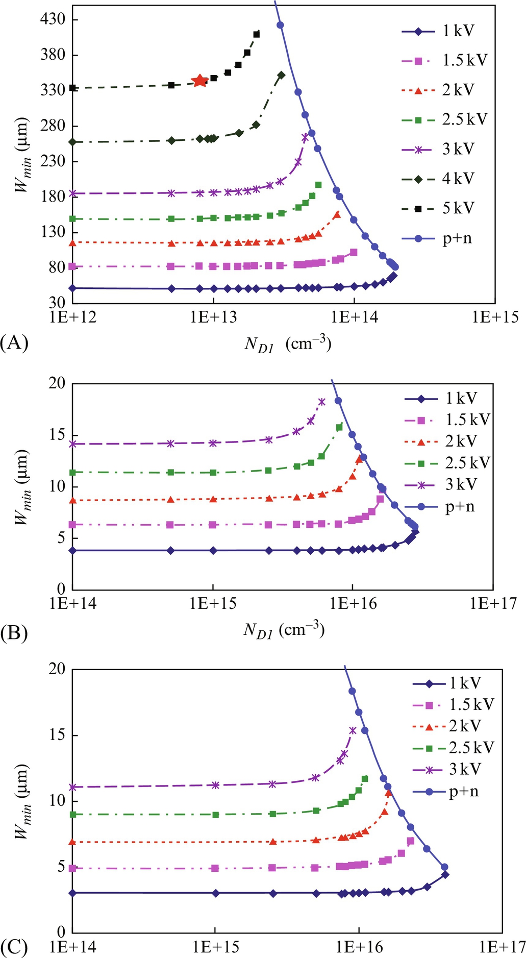
For the same breakdown voltage, the thickness of the lightly doped drift region N− of a GaN vertical PiN diode is smaller than the thickness of Si and SiC PiN diodes, while GaN PiN diodes can have a higher doping concentration in the lightly doped drift region than SiC and Si. Shown in Fig. 5.21 are the calculated results for the minimum width of the lightly doped drift region as a function of the doping concentration for a PiN structure for different applied voltages and different semiconductor materials: Si, 4H-SiC, and GaN [153]. For a 3 kV GaN diode, the thickness of the lightly doped drift region is ~12 μm, and the doping concentration for this thickness is ~1016 cm−3. For a SiC device, the thickness and the doping concentration for a 3 kV device are 15 μm and ~7×1015 cm−3, while for a Si device the thickness and the doping concentration for a 3 kV device are 200 μm and ~8×1013 cm−3. In [154], a vertical GaN 2.6 kV power diode is described with a lightly doped drift region width and doping concentration of 15 μm and ~8×1013 cm−3, which support the calculated results given in [153]. On the drift region, a heavily magnesium (Mg)-doped P+-type GaN layer is grown. The layer's impurity concentration is higher than 2×1017 cm−3, depending on the diode design.
A level-3 model introduced in Section 5.3.2.2 can be used for modeling a GaN PiN power diode. The most important parameter for a power GaN PiN diode is the voltage drop, VAK, across it during the conduction state. It is composed of five components, including the voltages across the junctions, J1 and J2; the voltage across the two depletion regions, Vd1 and Vd2; and the voltage across the drift region, ![]() :
:
Although the lightly doped drift region of a GaN PiN diode is significantly thinner than the lightly doped drift region of a Si PiN diode and the carrier concentration in the drift region is considerably higher in a GaN device, the voltage drop across a 5 kV GaN device, at a current smaller than 50 A, is larger than the voltage drop of a Si diode. The published data for the turn-ON voltage at room temperature of a GaN diode are larger than 3 V [150,155–157]. The reason for the higher turn-ON voltage of a GaN PiN diode is similar to the reason for that in a SiC PiN diode. SiC and GaN are wide bandgap materials, and their intrinsic carrier concentration, ni, at room temperature is significantly smaller than the carrier concentration of Si. The junction voltage of junction J1 is a dominant term in Eq. (5.192), especially for the diodes with a breakdown voltage smaller than 5 kV. The junction voltage of junction J1 is
where VT is the thermal voltage (kT/q), px1 is the excess carrier concentration of the lightly doped drift region at the junction J1, and ![]() is the doping concentration of the lightly doped drift region. The total junction voltage Vj12, which is a sum of the voltages of the junctions J1 and J2, Vj1 and Vj2:
is the doping concentration of the lightly doped drift region. The total junction voltage Vj12, which is a sum of the voltages of the junctions J1 and J2, Vj1 and Vj2:

The total junction voltage, Vj12, does not directly depend on the doping concentration of the lightly doped drift region, ![]() . However, there is a dependency between the boundary values of the excess charge concentrations, px1 and px2, and the impurity doping level that determines the junction voltage values. Also, the excess carrier concentrations, px1 and px2, depend on the emitter recombination parameters that can be assumed as constants for calculating the total forward voltage drop.
. However, there is a dependency between the boundary values of the excess charge concentrations, px1 and px2, and the impurity doping level that determines the junction voltage values. Also, the excess carrier concentrations, px1 and px2, depend on the emitter recombination parameters that can be assumed as constants for calculating the total forward voltage drop.
To obtain the minimum forward voltage drop, VAK, during conduction time, the minimum width of the drift region, corresponding to the minimum doping concentration, should be used. However, the results from the simulation given in [153] do not agree with this simple assertion. Increasing the doping concentration, ![]() ,for the same breakdown voltage leads to a decrease of VAK to a minimum value, after which further increases in the doping concentration cause an increase in the forward voltage drop. A higher doping concentration,
,for the same breakdown voltage leads to a decrease of VAK to a minimum value, after which further increases in the doping concentration cause an increase in the forward voltage drop. A higher doping concentration, ![]() , reduces the injection efficiencies of the higher doped P+ and N+ emitters into the drift region and, therefore, decreases the values of the excess carrier densities, px1 and px2, at the region boundaries. From Eq. (5.194), it can be seen that as the boundary charge concentrations are reduced, the total junction voltage, Vj12, also reduces, as shown in Fig. 5.22.
, reduces the injection efficiencies of the higher doped P+ and N+ emitters into the drift region and, therefore, decreases the values of the excess carrier densities, px1 and px2, at the region boundaries. From Eq. (5.194), it can be seen that as the boundary charge concentrations are reduced, the total junction voltage, Vj12, also reduces, as shown in Fig. 5.22.

 , as a function of the doping concentration of the lightly doped drift region,
  .
.Although higher doping concentrations, ![]() , lead to a decrease in the values of the excess carrier densities, px1 and px2, the voltage drop across the drift region,
, lead to a decrease in the values of the excess carrier densities, px1 and px2, the voltage drop across the drift region, ![]() , has a minimum value. The forward voltage drop, VAK, also has a minimum.
, has a minimum value. The forward voltage drop, VAK, also has a minimum.
The simulation results for optimizing the doping concentration to minimize the forward voltage drop, VAK, of a 5 kV Si PiN diode would lead to a reduction in the forward drop of more than 12%, while for SiC and GaN PiN diodes the reduction in the forward voltage drop for a concentration below 1015 cm−3 is <1% [153]. Hence, the optimization of the concentration of the lightly doped drift region for SiC and GaN is not necessary.
Fabricating GaN devices with high breakdown voltages requires a low-doped drift region and edge-termination (ET) structures that do not limit device performance. ET plays a key role in determining the device breakdown voltage. The purpose of the ET structures is to spread out the electric field at the edge of the junction such that there is no region with a very high electric field that can damage the device. The lack of good ET reduces the breakdown voltage significantly below the ideal limits due to field crowding at the edges that leads to an avalanche breakdown. To improve device performance, the electric field crowding at the edges should be minimized. Different ET techniques have been used for different types of GaN devices. One of them is smoothing of the equipotential contours at the edge of the device resulting in a manageable electric field [158]. A field-plate structure consisting of a SiNx passivation layer and a Ti/Au bilayer can be used for the ET [159]. When the metal contact is extended over a surface dielectric layer, for example, SiO2, the depletion region boundary is extended, and therefore, the electric field crowding is reduced [160]. Another ET technique for reducing electric field crowding is the formation of a P+ floating ring or guard ring [160]. In [161], a simple ET technique is used to achieve nearly ideal parallel plane breakdown voltage for GaN devices. The technique involves implanting a neutral species on the edges of devices to form a highly resistive, amorphous layer. ET is obtained by using argon implantation, increasing the breakdown voltage of GaN Schottky barrier diodes from 300 V for unterminated diodes to 1650 V after ET.
Improving the quality and the size of the GaN substrate, improving the quality of the epitaxial layers, and choosing the right ET technique will help the device designer to fabricate a high-voltage GaN PiN diode (>10 kV) that will switch quickly and have a smaller forward voltage drop than the Si PiN diode.
5.4.3 GaN JFET
The breakdown voltage of a lateral transistor depends mainly on the channel parameters. In order to maintain low ON-resistance, RON, the device width and the space between the gate and the drain should be increased, which limits the breakdown voltage to 1 kV and increases the need for more sophisticated device structures for managing the electric field and also increases the device capacitance. In a vertical device, the breakdown voltage depends on the deposition region parameters, and it is easier to scale up for high current and voltage. Vertical devices allow greater power density, lower capacitance, and generally better performance.
Two types of JFETs are considered in this book: a vertical JFET (VJEFT) and a lateral channel JFET with a vertical drift region (LC-VJFET).
5.4.3.1 Vertical JFET
Two cross sections of vertical GaN JFETs are depicted in Fig. 5.23. The first one has a rectangular channel, and the second has trapezoidal channels. Depending on the doping levels and physical dimensions of a VJFET, the transistor can be designed to operate as a normally-ON or normally-OFF device. A normally-OFF device is preferable because it will prevent current from flowing when no voltage is applied to the gate, and therefore, it can be easily utilized in power applications.

A cascode circuit, shown in Fig. 5.24, includes a high-voltage, normally-ON GaN JFET with a low-voltage MOSFET that can operate as a normally-OFF high-voltage device. The high-voltage GaN VJFET is a normally-ON device and has a negative threshold voltage, and the low-voltage MOSFET is capable of blocking ~30 V with a standard power MOSFET threshold voltage. The cascode circuit has the gate-driving characteristics of the standard power MOSFET and the current/voltage capability of the high-voltage GaN VJFET. Since the MOSFET is a low-voltage device, its ON-resistance, RDS_ON, is significantly smaller than in the GaN JFET, and the associated losses will be insignificant.
A VJFET consists of a heavily doped N+ region, a lightly doped N− drift region, and a channel region that is formed between two heavily doped P+ regions. On the top of the channel region is the heavily doped N+ region. For a normally-OFF device and with no voltage applied to the gates (VGS=0), the channel is fully depleted of carriers due to a significantly high doping concentration of the heavily doped P+ regions and the significantly low doping concentration in the channel. The depletion region width depends on the doping concentrations of the channel and heavily doped P+ region, NCH and NP; GaN permittivity, ɛ; built-in voltage, Vbi; and gate-source voltage, VGS:

The built-in voltage is calculated by the equation:

where k is Boltzmann's constant, T is the temperature in Kelvin, q is unit electric charge, and ni is the GaN intrinsic carrier concentration. If a positive voltage is applied to the gates, the depletion region width decreases, creating no resistive path for the current, and the current passes through the channel from the drain to the source.
For a normally-ON device and no voltage applied to the gates (VGS=0), the channel is not depleted, and the current passes through the channel from the drain to the source. When a negative voltage, with a magnitude higher than the threshold voltage, is applied to the gate, the depletion region is extended and prevents current from passing through the channel.
When a GaN VJFET is built on GaN substrate, the substrate has high electron concentration and plays the role as a heavily doped N+ region. Other substrates, such as Si or SiC, can be used for building of a GaN VJFET.
Epitaxial layers are grown on the top of the GaN substrate or the buffer layer for devices made with other substrates. The VJFET GaN epitaxial layers can have nonuniform doping concentration as a function of the thickness of the different layers, which can be used for optimizing a device's performance [162]. The drift region thickness and the doping concentration are designed to carry the majority of the drain-source voltage, VDS. The drift region concentration can be in the range of 1014–1016 cm−3. The gates are formed on the top of the heavily doped P+ regions, whose thickness, tCH, determines the channel thickness. The doping concentration in the channel can be equal to or less than the doping concentration of the drift region. The doping concentration in the channel depends on the desired threshold voltage of the VJFET.
In Fig. 5.23, the channel has a rectangular shape. There are JFETs where the channels can be designed to have a trapezoidal shape. The trapezoidal-shaped channel can improve the performance by enabling better control of the electric field near the location where the channel sidewall and the upper surface meet [162]. The width of the channel, WCH, for a rectangular channel or the bottom base for a trapezoidal-shaped channel can vary depending on numerous factors, such as desired functionality (normally-ON or normally-OFF device) and the channel doping concentration. The width and the thickness of the channel, WCH and tCH, should be optimized so that a very small leakage current flows from the source to the drain while maintaining a low ON-state resistance, RON.
Simulation results given in [163] showed that the ON-state resistance, RON, can be reduced by increasing the channel doping concentration and width, but in this case, the breakdown voltage is reduced, a positive threshold voltage is compromised, and a normally-OFF operation is hard to achieve. The threshold voltage, VT, is very sensitive to the channel width, WCH. In order to achieve a positive threshold voltage, VT, the channel width should be smaller than 1 μm, which leads to a high ON-state resistance, RON. To obtain a better trade-off between the threshold voltage, VT, and ON-state resistance, RON, a lateral channel JFET with a vertical drift region is proposed.
5.4.3.2 Lateral Channel JFET With Vertical Drift Region
A cross section of a lateral channel GaN JFET with a vertical drift region (LC VJFET) is shown in Fig. 5.25. Similar to VJFET, the doping levels and physical dimensions of an LC VJFET determine the transistor functionality to operate as a normally-ON or normally-OFF device. A normally-OFF device is preferable, but the cascode configuration shown in Fig. 5.24 has the gate-driving characteristic of the low-voltage MOSFET and the current/voltage capability of the high-voltage LC VJFET, which can be used for a normally-ON device.

The LC VJFET has three regions of interest. First is the core of the device, which includes the device channel and the gate region. The second region includes the lightly doped drift region and the substrate, and the third region is the edge termination and the isolation region.
A GaN LC VJFET can be built on a heavily doped GaN substrate, but other substrates, such as Si or SiC, can also be used. However, in this case, a buffer layer from AlN/GaN, AlGaN, or other suitable materials should be grown between the substrate and the epitaxial layer to improve the quality of the epitaxial layer grown on top of it. The breakdown voltage of an LC VJFET is determined by the doping concentration and thickness of the lightly doped drift region and also the proper edge-termination techniques. For a kV-rated device, the doping concentration of the lightly doped drift region is in the range of 1015–1016 cm−3. The lightly doped drift region provides a region through which current flows from the drain to source during the ON-state, but during the OFF-state, the drift region provides a region for supporting the electric field by the voltage gradient between the source or gate and the drain [164].
The channel of the LC-VJFET is composed of two parts: a vertical and a lateral conductive region. A blocking P-type GaN layer, with a significantly high impurity concentration in the range of 1017–1019 cm−3, is used to form the two regions. The blocking layer supports the vertical electric field and causes the current to flow in the lateral area of the channel. The length of the overlap, LGOL, between the gate and the blocking layer is an important parameter. This is exactly the effective gate that modulates the lateral channel width and changes the conductivity of the channel. When the length of the overlap, LGOL, is smaller than the optimum value, leakage current in the device increases as the channel is not fully pinched OFF, and some electrons flow from the source to the drain. But increasing the length of the overlap, LGOL, more than the optimum value causes the ON-state resistance of the device to increase [163].
The vertical channel region is a continuation of the lightly doped drift region. The vertical channel thickness and doping concentration should be optimized with two constraints: minimizing the LC-VJFET ON-resistance when the device is turned ON and providing proper pinch-OFF so that no current passes through the channel when the device is turned OFF. The channel width, WCH, is also an important design parameter that determines the functionality of the device as a normally-ON or normally-OFF design. If the channel width, WCH, is significantly large, the path of the current from the drain to the source will be low resistance, but in this circumstance, pinch-OFF of the channel is more difficult to achieve.
On the top of the channel, a heavily doped P+-type GaN layer is deposited and patterned to form the gate. The blocking P-type GaN layer, together with the gate, can control the device by the PN junctions formed with the N-type channel. In some designs, the gate and the blocking layer are electrically tied to form a buried P-type gate.
The edge-termination scheme used in the transistors is similar to those schemes used in PiN junction diodes. The potential applied to the top metal is spread over a distance that is typically greater than the thickness of the lightly doped drift region. For this purpose, two separate implant steps are used. Smoothing the equipotential contours at the device edges results in better management of the electric field on the device surface and prevents the device from breaking down prematurely [165]. In this case, if a breakdown occurs, it will be due to an avalanche breakdown.
The operation of an LC-VJFET depends on the design. For a normally-OFF device, where no voltage is applied to the gates (VGS=0), the channel is fully depleted of carriers due to a significantly high doping concentration of the heavily doped P+ gate and the blocking P-type GaN layer from one side and a significantly low doping concentration in the channel from the other side. Two depletion regions are formed: one from the PN junction of the P+ gate and the N-channel and the second one from the blocking P-type GaN layer and the N-channel. The two depletion widths can be calculated using Eq. (5.195) by substituting the corresponding doped concentrations. The total depletion width, W, is a sum of the depletion width of the two junctions. When a positive voltage is applied to the gates, the depletion width, W, decreases, and current passes through the channel from the drain to the source. For a normally-ON device with no voltage applied to the gates (VGS=0), the channel is not depleted, and the current flows through the channel from the drain to the source. When a negative voltage, with a magnitude higher than the threshold voltage, is applied to the gate, the two depletion regions are expanded and prevent current from passing through the channel.
The simulation results given in [163] show that there is a higher degree of coupling between the ON-resistance, RON, and the threshold voltage, VT, in the LC VJFET than in the VJFET. Therefore, a low ON-state resistance can be obtained with a thinner and more highly doped N-GaN channel.
5.4.4 GaN MOSFET
In the last 10 years, research on the design, fabrication, and characterization of high-voltage GaN MOSFETs has been based on both lateral and vertical structures: the fabrication process for a lateral high-voltage MOSFET is simpler than the vertical MOSFET since a thick, lightly doped drift region is necessary for a vertical structure. For the same breakdown voltage, a lateral device has a larger area than a vertical device. Therefore, the chip size of a lateral MOSFET is bigger. However, a Si substrate can be used for growth of lateral devices, which are larger and cheaper, while GaN substrates are normally used for vertical MOSFETs, which are smaller and more expensive. Other substrates, such as Si or SiC can also be used for vertical devices, but a buffer layer should be grown between the substrate and the epitaxial layer to improve the quality of the epitaxial layer, which increases the device cost.
5.4.4.1 Vertical Trench MOSFET
Fig. 5.26 shows a cross section of a high-voltage GaN vertical trench MOSFET. Most of the vertical GaN high-voltage MOSFETs are built on a low-defect-density GaN substrate, which is the MOSFET drain. The substrate doping concentration is higher than 1018 cm−3. A lightly doped N− drift region is grown on the top of the substrate by metal-organic vapor deposition. The doping concentration of the drift region is in the range of 1014–1016 cm−3, and its thickness depends on the desired breakdown voltage. The area of the drift region depends on its thickness. It should be chosen to allow spreading of the current in the drift region, thereby decreasing the drift region ON-resistance. The value of the thickness and the doping concentration of the lightly doped drift region can be optimized so that the sum of the conduction and the switching losses of the device can be minimized.

A P-type base layer with a thickness smaller than 1 μm is grown on the top of the drift region. The thickness of the P-layer is the channel length of the device or the effective gate of the device. The doping concentration of the base is higher than the drift region, and it is in the range of 1017–1019 cm−3. On the top of the base layer, a selective area regrowth of a heavily doped N+-type layer is grown to form the MOSFET source. SiO2 can be used as the regrowth mask. The doping concentration of the N+-type layer is higher than 3×1018 cm−3, and the thickness is smaller than 0.5 μm. Usually for GaN devices, Si is used as the dopant for the formation of N-type layers, and Mg is used for P-type.
The gate trench is then formed by etching part of the two MOSFET layers, P base and N+ source. A SiO2 layer, as a dielectric interlayer, is deposited on the sidewall and the bottom of the trench by plasma-enhanced chemical vapor deposition, and then, the metal is deposited to form the gate electrode. The vertical sidewall of the trench should be well smoothed and cleaned to achieve high inversion layer mobility and, therefore, low resistivity of the channel [38]. Also, the trench bottom plays a crucial role in achieving superior electric performance and highly reliable operation. Therefore, the trench bottom should be a little bit rounded, which will reduce the P-well pinching effect, and as a result, the pinching resistance under the gate-drain area is decreased [166].
To improve the OFF-state characteristic, such as the breakdown voltage of a trench MOSFET, a field-plate edge-termination technique can be used to reduce the electric field at the edge of the PN junction around the isolation mesa periphery [167]. The field plate consists of the extended wiring electrode for the source electrode. The field-plate electrode completely overlaps the PN junction from the side, and therefore, the potential crowding at the edge of the PN junction is effectively reduced. While an improvement of the ON-state characteristic, such as the ON-resistance can be achieved by reducing the cell pitch size, improving the dielectric/semiconductor interface quality, and optimizing the drift layer growth condition which will enhance the electron mobility.
The operation of a high-voltage GaN trench MOSFET is similar to the operation of Si and SiC trench MOSFETs. When a positive voltage higher than the threshold voltage is applied between the gate and the source of the device, an N-channel region is formed on the surface of the P base that provides a conducting path between the source and drain terminals. If the gate to source voltage is below the threshold voltage, the transistor is turned off, and only a very small leakage current is passing from the drain to the source of the transistor. In theory, the threshold voltage of a MOSFET is defined as the voltage applied between the gate and source that creates an inversion layer of minority carriers with a concentration higher than the base. According to [168], the threshold voltage is

where ɛGaN and ![]() are the permittivity of GaN and SiO2, respectively;,
are the permittivity of GaN and SiO2, respectively;, ![]() is the thickness of the SiO2; and NP is the doping concentration of the base. The surface potential at the P base is ΦS. At the deposition-inversion transition point, the surface potential is
is the thickness of the SiO2; and NP is the doping concentration of the base. The surface potential at the P base is ΦS. At the deposition-inversion transition point, the surface potential is

For the same doping concentration of the P base and SiO2 layer thickness, the calculated threshold voltage for a GaN device should be larger than the threshold voltages of SiC and Si devices because of the significantly low intrinsic carrier concentration of GaN. The simulation result for the threshold voltage of a trench GaN MOSFET (P-base doping concentration 3×1019 cm−3) obtained from a one-dimensional, self-consistent Schrödinger-Poisson solver is 26 V, while the experimental result for the same device is significantly lower at 8 V [169]. Other researchers, [170–172], have also reported low experimental threshold voltage values compared with theoretical values. Differences between the simulation and experimental results can be due to the sidewall etch damage of the P base, which can cause nitrogen vacancies to form and behave as donors [169]. Research about decreasing the sidewall etch damage, better smoothing, and cleaning after sidewall etching is being conducted, which will increase the threshold voltage and provide better noise immunity to prevent false turn-on.
In 2016, at the 28th International Symposium on Power Semiconductor Devices and ICs, a state-of-the-art GaN trench MOSFET, with a breakdown voltage of 1.6 kV and a high current operation exceeding 10 A for a single-cell device, was reported [167]. The breakdown voltage of the device was improved from 1.2 to 1.6 kV by applying a field-plate edge-termination technique around the isolation mesa of the transistor. The specific ON-resistance, RON, of the single cell, measured when a gate-source voltage, VGS, of 40 V was applied, was 2.7 mΩ cm2. The threshold voltage of the trench MOSFET was reported to be 3.5 V. The authors also showed the switching characteristics for a double-pulse switching experiment (see Fig. 5.27). From the switching characteristics, the rise and fall time, tr and tf, were determined to be 19 and 10 ns, respectively, when the supply voltage, VDD, was 400 V and the drain current, ID, was around 10–14 A. Also, the turn-on and turn-off switching losses were calculated to be 90 and 12 μJ, respectively, which suggests that the fabricated vertical GaN trench MOSFETs are suitable for use in high-power applications with high-frequency switching.
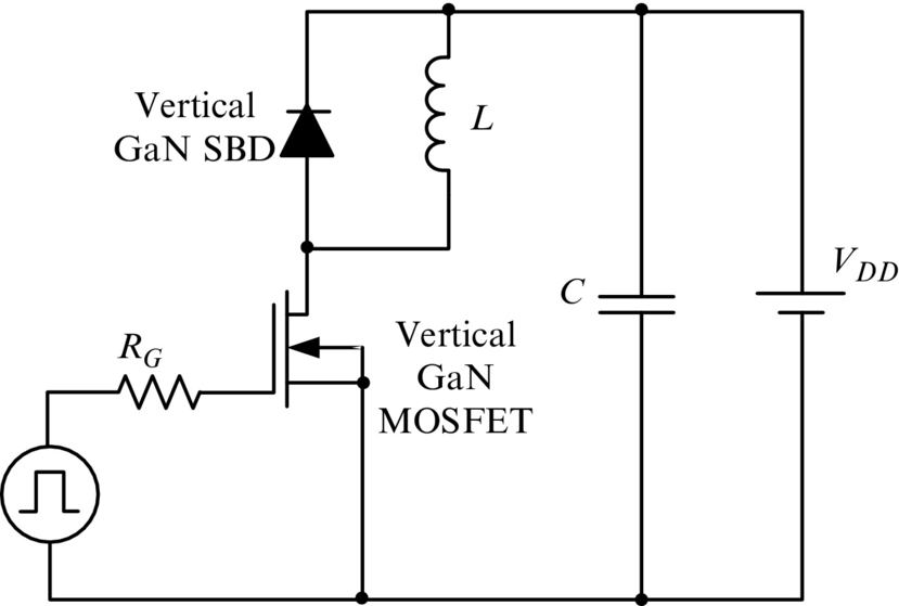
5.4.4.2 Lateral MOSFET
Lateral MOSFETs have a significantly simpler structure than the vertical ones because during fabrication, no heavy etching is used for the gate and no thick, lightly doped drift region is grown. Also, the three terminals, the source, gate, and drain, are placed on the top surface, which is suitable for power-integrated circuits where the power transistor is monolithically integrated with control circuits on the same chip. However, for the same blocking voltage, the length of the channel of a lateral MOSFET is longer, and therefore, the area of the device is larger than the area of a vertical trench MOSFET. Similar to the vertical MOSFET, the lateral MOSFET is normally an OFF device.
A cross section of a GaN lateral MOSFET is shown in Fig. 5.28. Different substrates, such as sapphire, SiC, and GaN, have been used for fabricating lateral MOSFETs. A P-type Mg-doped GaN layer is grown by metal-organic chemical vapor deposition on top of the substrate. For better growth of the P-doped layer, a buffer layer between the substrate and the P layer is grown. A SiO2 thin layer is grown on top of the P layer to form the MOS structure of the transistor and to suppress any damage or pollution due to ion implantation. The ion implantation is used to place Si ions in the P layer and to form heavily doped N+ source and drain regions. In the end, low-resistance contact layers are formed on the drain, source, and the gate.

The breakdown of a lateral MOSFET is mainly determined by the thickness of the SiO2 layer. Since the drain has a high doping concentration, the voltage drop of the drain region is significantly smaller. Therefore, the potential of the region of the drain under the gate is approximately equal to the applied voltage on the drain. When the gate-source voltage is smaller than the threshold voltage and the drain-source voltage is significantly high, a breakdown can occur in the gate oxide. A schematic of a lateral GaN MOSFET during the OFF-state and its potential and electric field in function of the position is shown in Fig. 5.29. During the OFF-state, the gate and source are connected to the ground, and high voltage is applied to the drain with respect to the source. The electric field between the drain and the gate is significantly high because of the small thickness of the SiO2 layer, while the channel length is significantly larger. Therefore, the electric field between the drain and source is smaller. Also, the resistance of the SiO2 layer is larger than the channel resistance. For these reasons, almost all of the electric field is concentrated on the gate oxide, a result of the breakdown near point 1 in Fig. 5.29 [173].
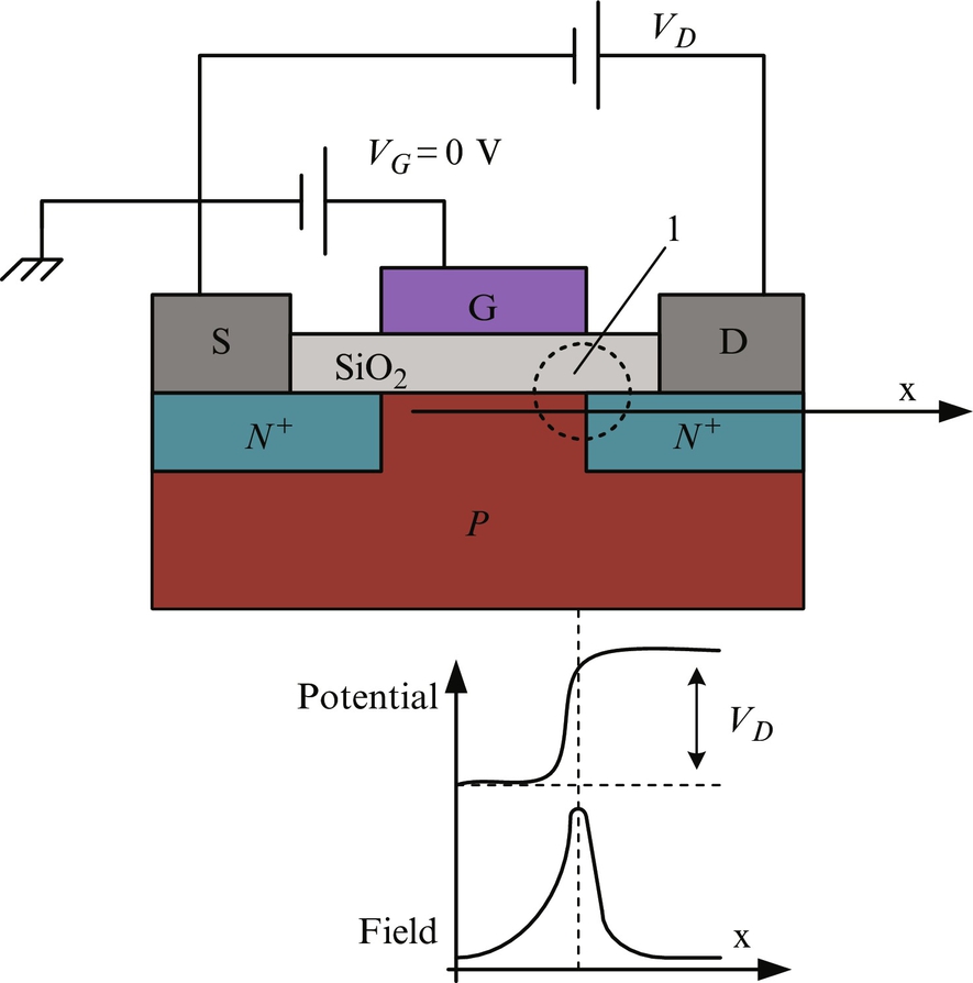
The electric field in the region between the gate and the drain is significantly higher and, therefore, limits the voltage applied between the drain and the source. To spread the electric field and decrease its value in the region between the gate and the drain, a lightly doped N− layer, known as the reduced surface field (RESURF) layer, is used by different scientific groups to increase the breakdown voltage of a lateral device. The RESURF concept was introduced by Appels and Vaes for the first time [174]. A RESURF layer increases the breakdown voltage of lateral MOSFETs and increases the ON-state resistance since the layer should be long and lightly doped. Another aspect of a long, lateral drift layer is the additional required chip area, which increases the cost of the devices. For a given breakdown voltage, the optimal parameters of a RESURF layer, the length and doping concentration, should be determined. A trade-off between blocking voltage and ON-state resistance should be found.
A lateral GaN MOSFET with a RESURF layer during the OFF-state and its potential and electric field as a function of the position is shown in Fig. 5.30. During the OFF-state, a big part of the electric field of the MOSFET with a RESURF layer is concentrated on the two sides of the RESURF layer, and some part is in the RESURF layer. Therefore, for the same breakdown voltage, the electric field in the gate oxide layer for a MOSFET with a RESURF layer will be significantly smaller than the electric field in the gate oxide layer for a conventional MOSFET. To ensure long-term reliability of a MOSFET, the electric field in the gate oxide layer should be kept below 3 MV cm−1. A lateral GaN MOSFET with RESURF, with a high blocking capability of 1550 V and an operation current of 2.5 A, is reported in [172]. To further reduce the surface electric field and maintain a high breakdown voltage, two RESURF regions are required. A lateral GaN with two RESURF regions is shown in Fig. 5.31. The RESURF1 region is near the gate and has a low implant dose. Lowering the implant dose in RESURF1 will reduce the electric field of the oxide near to the gate. The RESURF2 region is near the drain and has a high implant dose. The higher implant dose in the RESURF2 region will support high breakdown voltage. In [175], an enhancement mode N-channel lateral GaN high-voltage MOSFET with two RESURF regions is presented, with a breakdown voltage of 2.5 kV and a specific on-resistance of 30 mΩ cm−2. Further improvement of lateral GaN MOSFETs can be accomplished by improving the quality of the SiO2/GaN interface and reducing the resistance of the contacts. If the SiO2/GaN interface has poor quality, the electrons passing through the channel are captured at interface states leading to a decrease in electron mobility and, therefore, an increase in channel resistance. Annealing at temperatures higher than 900°C after depositing SiO2 has been used to decrease interface state density [173,176,177].


Simulation results for GaN MOSFET devices of similar dimension with a RESURF region (field-plate structure) and a GaN HEMT are given in [177]. From the simulation results, it is concluded that both devices are capable of producing similar ON-state modes of operation and achieve similar effective mobility at equivalently larger electric fields. However, during subthreshold operation, the GaN MOSFET is shown to contain a much lower carrier concentration than the GaN heterostructure field-effect transistor (HFET). As a result, the breakdown avalanche effect in the GaN MOSFET is roughly five times larger than the GaN HFET for devices of similar dimensions, 3500 and 600 V, respectively. Therefore, implementing the MOS structure with the high quality of the SiO2/GaN interface can potentially resolve fundamental constraints for high-voltage power applications caused by current device architects.