Resonant and Soft-Switching Converters
Muhammad H. Rashid Florida Polytechnic University, Lakeland, FL, United States
Shu Yuen (Ron) Hui The University of Hong Kong, Pokfulam, Hong Kong
Henry Shu-Hung Chung City University of Hong Kong, Kowloon, Hong Kong
Abstract
Advances in power electronics in the last few decades have led to not only just improvements in power devices but also new concepts in converter topologies, modulations, and control strategies. In the 1970s, conventional pulse-width modulation (PWM) power converters were operated in a switched-mode operation. Due to the nonideal switching characteristics, power switches have to switch their currents within the turn-on and turn-off times under the hard-switching conditions, causing undesired voltage and current stresses. More importantly, hard switching would cause high power and heat dissipation, introducing many reliability problems. In order to reduce the switching losses and improve the conversion efficiency, various resonant and soft-switching techniques have been proposed and widely used in various power electronic applications. The basic concept is to introduce an extra circuit, utilize parasitic elements, and/or timing control to profile switching trajectories, so that the switches are switched softly. This chapter gives an overview of various resonant and soft-switching techniques, such as zero-voltage switching, zero-current switching, zero-voltage transition, series resonance, and parallel resonance. It will start from describing the basic principles of those techniques to their applications to various systems, such as DC-DC power conversion and DC-AC power conversion. The electromagnetic compatibility performance will also be addressed. The emphasis is placed on the basic operating principle and practicality of the converters without using much mathematical analysis.
Keywords
Resonant converters; Soft switching; Zero-voltage switching; Zero-current switching; DC-DC power conversion; DC-AC power conversion
12.1 Introduction
Advances in power electronics in the last few decades have led to not only improvements in power devices but also new concepts in converter topologies and control. In the 1970s, conventional pulse-width modulation (PWM) power converters were operated in a switched-mode operation. Power switches have to cut off the load current within the turn-on and turn-off times under the hard-switching conditions. Hard switching refers to the stressful switching behavior of the power electronic devices. The switching trajectory of a hard-switched power device is shown in Fig. 12.1. During the turn-on and turn-off processes, the power device has to withstand high voltage and current simultaneously, resulting in high switching losses and stress.
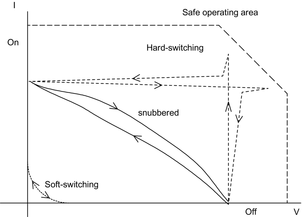
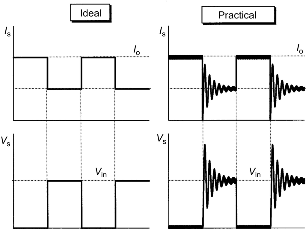
Dissipative passive snubbers are usually added to the power circuits so that the dv/dt and di/dt of the power devices could be reduced and the switching loss and stress be diverted to the passive snubber circuits. However, the switching loss is proportional to the switching frequency, thus limiting the maximum switching frequency of the power converters. Typical converter switching frequency was limited to a few tens of kilohertz (typically 20–50 kHz) in the early 1980s. The stray inductive and capacitive components in the power circuits and power devices still cause considerable transient effects, which in turn give rise to electromagnetic interference (EMI) problems. Fig. 12.2 shows ideal switching waveforms and typical practical waveforms of the switch voltage. The transient ringing effects are major causes of EMI.
In the 1980s, lots of research efforts were diverted toward the use of resonant converters. The concept was to incorporate resonant tanks in the converters to create oscillatory (usually sinusoidal) voltage and/or current waveforms so that zero-voltage switching (ZVS) or zero-current switching (ZCS) conditions can be created for the power switches. The reduction of switching loss and the continual improvement of power switches allow the switching frequency of the resonant converters to reach hundreds of kilohertz (typically 100–500 kHz). Consequently, the size of magnetic components can be reduced, and the power density of the converters increased. Various forms of resonant converters have been proposed and developed. However, most of the resonant converters suffer several problems. When compared with the conventional PWM converters, the resonant current and the voltage of resonant converters have high peak values, leading to higher conduction loss and higher V and I rating requirements for the power devices. Also, many resonant converters require frequency modulation (FM) for output regulation. Variable switching frequency operation makes the filter design and control more complicated.
In the late 1980s and throughout the 1990s, further improvements have been made in converter technology. New generations of soft-switched converters that combine the advantages of conventional PWM converters and resonant converters have been developed. These soft-switched converters have switching waveforms similar to those of conventional PWM converters except that the rising and falling edges of the waveforms are “smoothed” with no transient spikes. Unlike the resonant converters, new soft-switched converters usually utilize the resonance in a controlled manner. Resonance is allowed to occur just before and during the turn-on and turn-off processes so as to create ZVS and ZCS conditions. Other than that, they behave just like conventional PWM converters. With simple modifications, many customized control integrated circuits (ICs) designed for conventional converters can be employed for soft-switched converters. Because the switching loss and stress have been reduced, soft-switched converter can be operated at the very high frequency (typically 500 kHz to a few megahertz). Soft-switching converters also provide an effective solution to suppress EMI and have been applied to DC-DC, AC-DC, and DC-AC converters. This chapter covers the basic technology of resonant and soft-switching converters. Various forms of soft-switching techniques such as ZVS, ZCS, voltage clamping, and zero-voltage transition methods are addressed. The emphasis is placed on the basic operating principle and practicality of the converters without using much mathematical analysis.
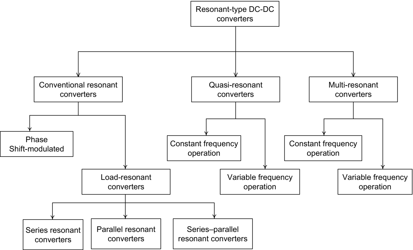
12.2 Classification
12.3 Resonant Switch
Prior to the availability of fully controllable power switches, thyristors were the major power devices used in power electronic circuits. Each thyristor requires a commutation circuit, which usually consists of an LC resonant circuit, for forcing the current to zero in the turn-off process [1]. This mechanism is in fact a type of zero-current turn-off process. With the recent advancement in semiconductor technology, the voltage and current handling capability and the switching speed of fully controllable switches have significantly been improved. In many high-power applications, controllable switches such as gate turn-offs (GTOs) and insulated-gate bipolar transistors (IGBTs) have replaced thyristors [2,3]. However, the use of resonant circuit for achieving ZCS and/or ZVS [4–8] has also emerged as a new technology for power converters. The concept of resonant switch that replaces conventional power switch is introduced in this section.
A resonant switch is a subcircuit comprising a semiconductor switch S and resonant elements, Lr and Cr [9–11]. The switch S can be implemented by a unidirectional or bidirectional switch, which determines the operation mode of the resonant switch. Two types of resonant switches [12], including zero-current (ZC) resonant switch and zero-voltage (ZV) resonant switches, are shown in Figs. 12.3 and 12.4, respectively.

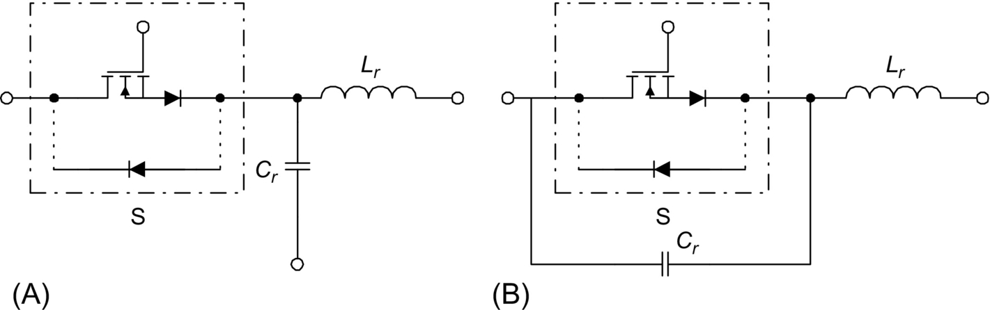
12.3.1 ZC Resonant Switch
In a ZC resonant switch, an inductor Lr is connected in series with a power switch S in order to achieve zero-current switching (ZCS). If the switch S is a unidirectional switch, the switch current is allowed to resonate in the positive half cycle only. The resonant switch is said to operate in half-wave mode. If a diode is connected in antiparallel with the unidirectional switch, the switch current can flow in both directions. In this case, the resonant switch can operate in full-wave mode. At turn-on, the switch current will rise slowly from zero. It will then oscillate, because of the resonance between Lr and Cr. Finally, the switch can be commutated at the next zero-current duration. The objective of this type of switch is to shape the switch current waveform during conduction time in order to create a zero-current condition for the switch to turn off [13].
12.3.2 ZV Resonant Switch
In a ZV resonant switch, a capacitor Cr is connected in parallel with the switch S for achieving zero-voltage switching (ZVS). If the switch S is a unidirectional switch, the voltage across the capacitor Cr can oscillate freely in both positive and negative half cycle. Thus, the resonant switch can operate in full-wave mode. If a diode is connected in antiparallel with the unidirectional switch, the resonant capacitor voltage is clamped by the diode to zero during the negative half cycle. The resonant switch will then operate in half-wave mode. The objective of a ZV switch is to use the resonant circuit to shape the switch voltage waveform during the off time in order to create a zero-voltage condition for the switch to turn on [13].
12.4 Quasi-Resonant Converters
Quasi-resonant converters (QRCs) can be considered as a hybrid of resonant and PWM converters. The underlying principle is to replace the power switch in PWM converters with the resonant switch. A large family of conventional converter circuits can be transformed into their resonant converter counterparts. The switch current and/or voltage waveforms are forced to oscillate in a quasi-sinusoidal manner, so that ZCS and/or ZVS can be achieved. Both ZCS-QRCs and ZVS-QRCs have half-wave and full-wave mode of operations [8–10,12].
12.4.1 ZCS-QRCs
A ZCS-QRC designed for half-wave operation is illustrated with a buck-type DC-DC converter. The schematic is shown in Fig. 12.5A. It is formed by replacing the power switch in conventional PWM buck converter with the ZC resonant switch in Fig. 12.3A. The circuit waveforms in steady state are shown in Fig. 12.5B. The output filter inductor Lf is sufficiently large so that its current is approximately constant. Prior to turning the switch on, the output current Io freewheels through the output diode Df. The resonant capacitor voltage VCr equals zero. At t0, the switch is turned on with ZCS. A quasi-sinusoidal current IS flows through Lr and Cr, the output filter, and the load. S is then softly commutated at t1 with ZCS again. During and after the gate pulse, the resonant capacitor voltage VCr rises and then decays at a rate depending on the output current. Output voltage regulation is achieved by controlling the switching frequency. Operation and characteristics of the converter depend mainly on the design of the resonant circuit Lr Cr. The following parameters are defined: voltage conversion ratio M, characteristic impedance Zr, resonant frequency fr, normalized load resistance r, and normalized switching frequency γ:
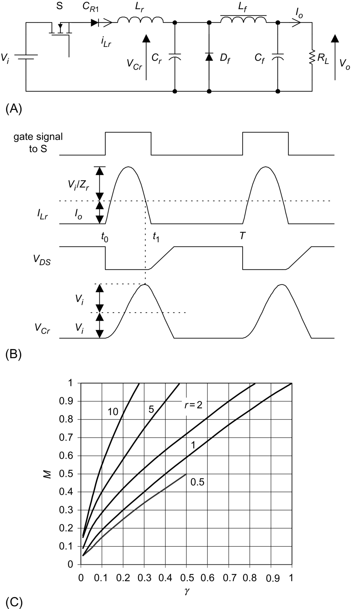


It can be seen from the waveforms that if Io>Vi/Zr, IS will not come back to zero naturally and the switch will have to be forced off, thus resulting in turn-off losses.
The relationships between M and γ at different r are shown in Fig. 12.5C. It can be seen that M is sensitive to the load variation. At light-load conditions, the unused energy is stored in Cr, leading to an increase in the output voltage. Thus, the switching frequency has to be controlled, in order to regulate the output voltage.
If an antiparallel diode is connected across the switch, the converter will be operating in full-wave mode. The circuit schematic is shown in Fig. 12.6A. The circuit waveforms in steady state are shown in Fig. 12.6B. The operation is similar to the one in half-wave mode. However, the inductor current is allowed to reverse through the antiparallel diode, and the duration for the resonant stage is lengthened. This permits excess energy in the resonant circuit at light loads to be transferred back to the voltage source Vi. This significantly reduces the dependence of Vo on the output load. The relationships between M and γ at different r are shown in Fig. 12.6C. It can be seen that M is insensitive to load variation.

By replacing the switch in the conventional converters, a family of QRC [9] with ZCS is shown in Fig. 12.7.

12.4.2 ZVS-QRC
In these converters, the resonant capacitor provides a zero-voltage condition for the switch to turn on and off. A quasi-resonant buck converter designed for half-wave operation is shown in Fig. 12.8A—using a ZV resonant switch in Fig. 12.4B. The steady-state circuit waveforms are shown in Fig. 12.8B. Basic relations of ZVS-QRCs are given in Eqs. (12.1A)–(12.1E). When the switch S is turned on, it carries the output current Io. The supply voltage Vi reverse biases the diode Df. When the switch is zero-voltage (ZV) turned off, the output current starts to flow through the resonant capacitor Cr. When the resonant capacitor voltage VCr is equal to Vi, Df turns on. This starts the resonant stage. When VCr equals zero, the antiparallel diode turns on. The resonant capacitor is shorted, and the source voltage is applied to the resonant inductor Lr. The resonant inductor current ILr increases linearly until it reaches Io. Then, Df turns off. In order to achieve ZVS, S should be triggered during the time when the antiparallel diode conducts. It can be seen from the waveforms that the peak amplitude of the resonant capacitor voltage should be greater or equal to the input voltage (i.e., IoZr>Vin). From Fig. 12.8C, it can be seen that the voltage conversion ratio is load-sensitive. In order to regulate the output voltage for different loads r, the switching frequency should also be changed accordingly.

ZVS converters can be operated in full-wave mode. The circuit schematic is shown in Fig. 12.9A. The circuit waveforms in steady state are shown in Fig. 12.9B. The operation is similar to half-wave mode of operation, except that VCr can swing between positive and negative voltages. The relationships between M and γ at different r are shown in Fig. 12.9C.

Comparing Fig. 12.8C with Fig. 12.9C, it can be seen that M is load-insensitive in full-wave mode. This is a desirable feature. However, as the series diode limits the direction of the switch current, energy will be stored in the output capacitance of the switch and will dissipate in the switch during turn-on. Hence, the full-wave mode has the problem of capacitive turn-on loss and is less practical in high-frequency operation. In practice, ZVS-QRCs are usually operated in half-wave mode rather than full-wave mode.
By replacing the ZV resonant switch in the conventional converters, various ZVS-QRCs can be derived. They are shown in Fig. 12.10.

12.4.3 Comparisons Between ZCS and ZVS
ZCS can eliminate the switching losses at turnoff and reduce the switching losses at turn-on. As a relatively large capacitor is connected across the output diode during resonance, the converter operation becomes insensitive to the diode's junction capacitance. When power MOSFETs are zero-current switched on, the energy stored in the device's capacitance will be dissipated. This capacitive turn-on loss is proportional to the switching frequency. During turn-on, considerable rate of change of voltage can be coupled to the gate drive circuit through the Miller capacitor, thus increasing switching loss and noise. Another limitation is that the switches are under high current stress, resulting in higher conduction loss. However, it should be noted that ZCS is particularly effective in reducing switching loss for power devices (such as IGBT) with large tail current in the turn-off process.
ZVS eliminates the capacitive turn-on loss. It is suitable for high-frequency operation. For single-ended configuration, the switches could suffer from excessive voltage stress, which is proportional to the load. It will be shown in Section 12.5 that the maximum voltage across switches in half-bridge and full-bridge configurations is clamped to the input voltage.
For both ZCS and ZVS, the output regulation of the resonant converters can be achieved by variable frequency control. ZCS operates with constant on-time control, while ZVS operates with constant off-time control. With a wide input and load range, both techniques have to operate with a wide switching frequency range, making it not easy to design resonant converters optimally.
12.5 ZVS in High Frequency Applications
By the nature of the resonant tank and ZCS, the peak switch current in resonant converters is much higher than that in the square-wave counterparts. In addition, a high voltage will be established across the switch in the off state after the resonant stage. When the switch is switched on again, the energy stored in the output capacitor will be discharged through the switch, causing a significant power loss at high frequencies and high voltages. This switching loss can be reduced by using ZVS.
ZVS can be viewed as square-wave power utilizing a constant off-time control. Output regulation is achieved by controlling the on-time or switching frequency. During the off time, the resonant tank circuit traverses the voltage across the switch from zero to its peak value and then back to zero again. At that ZV instant, the switch can be reactivated. Apart from the conventional single-ended converters, some other examples of converters with ZVS are illustrated in the following section.
12.5.1 ZVS With Clamped Voltage
The high voltage stress problem in the single-switch configuration with ZVS can be avoided in half-bridge (HB) and full-bridge (FB) configurations [14–17]. The peak switch voltage can be clamped to the DC supply rail, thus reducing the switch voltage stress. In addition, the series transformer leakage and circuit inductance can form parts of the resonant path. Therefore, these parasitic components, which are undesirable in hard-switched converter, become useful components in ZVS ones. Figs. 12.11 and 12.12 show the ZVS HB and FB circuits, respectively, together with the circuit waveforms. The resonant capacitor is equivalent to the parallel connection of the two capacitors (Cr/2) across the switches. The off-state voltage of the switches will not exceed the input voltage during resonance because they will be clamped to the supply rail by the antiparallel diode of the switches.


12.5.2 Phase-shifted Converter With Zero Voltage Transition
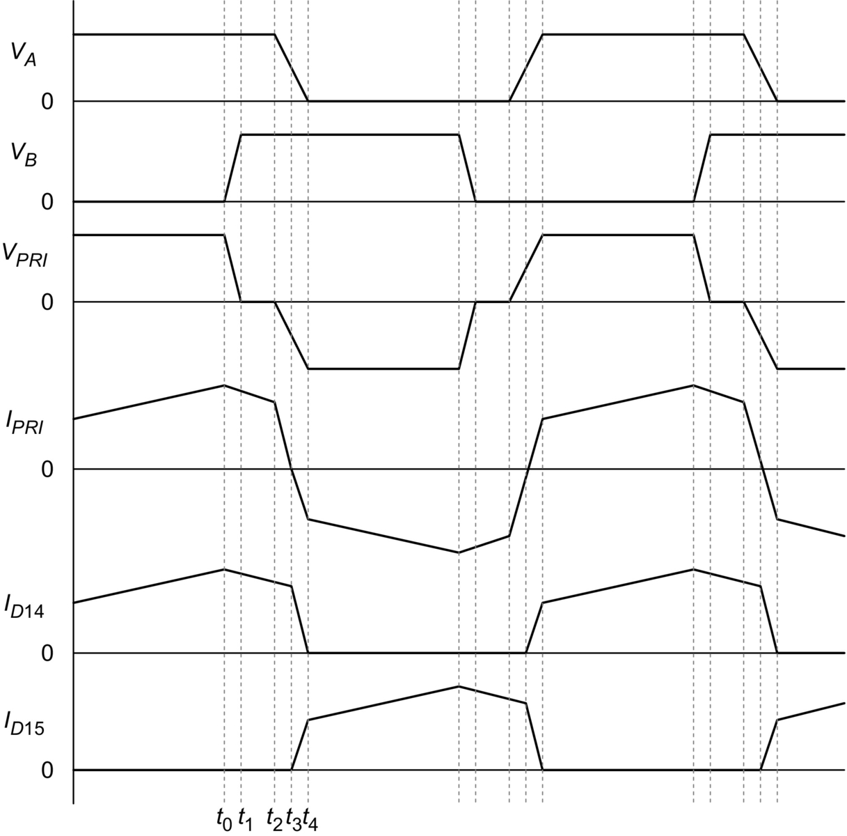
In a conventional FB converter, the two diagonal switch pairs are driven alternatively. The output transformer is fed with an AC rectangular voltage. By applying a phase-shifting approach, a deliberate delay can be introduced between the gate signals and the switches [18]. The circuit waveforms are shown in Fig. 12.13. Two upper or lower switches can be conducting (either through the switch or the antiparallel diode), yet the applied voltage to the transformer is zero. This zero-voltage condition appears in the interval [t1, t2] of Vpri in Fig. 12.13. This operating stage corresponds to the required off time for that particular switching cycle. When the desired switch is turned off, the primary transformer current flows into the switch output capacitance causing the switch voltage to resonate to the opposite input rail. Effects of the parasitic circuit components are used advantageously to facilitate the resonant transitions. This enables a ZVS condition for turning on the opposite switch. Thus, varying the phase shift controls the effective duty cycle and hence the output power. The resonant circuit is necessary to meet the requirement of providing sufficient inductive energy to drive the capacitors to the opposite bus rail. The resonant transition must be achieved within the designed transition time.
12.6 Multi-resonant Converters
The ZCS-QRCs and ZVS-QRCs optimize the switching condition for either the active switch or the output diode only, but not for both of them simultaneously. Multiresonant switch concept, which is an extension of the concept of the resonant switch, has been developed to overcome such limitation. The zero-current multiresonant (ZC-MR) and zero-voltage multiresonant (ZV-MR) switches [12,17] are shown in Fig. 12.14.

The multiresonant circuits incorporate all major parasitic components, including switch output capacitance, diode junction capacitance, and transformer leakage inductance into the resonant circuit. In general, ZVS (half-wave mode) is more favorable than ZCS in DC-DC converters for high-frequency operation because the parasitic capacitance of the active switch and the diode will form a part of the resonant circuit.
An example of a buck ZVS-MRC is shown in Fig. 12.15. Depending on the ratio of the resonant capacitance CD/CS, two possible topological modes, namely, mode I and mode II, can be operated [19]. The ratio affects the time at which the voltages across the switch S and the output diode Df become zero. Their waveforms are shown in Fig. 12.16A and B, respectively. If diode voltage VD falls to zero earlier than the switch voltage VS, the converter will follow mode I. Otherwise, the converter will follow mode II.
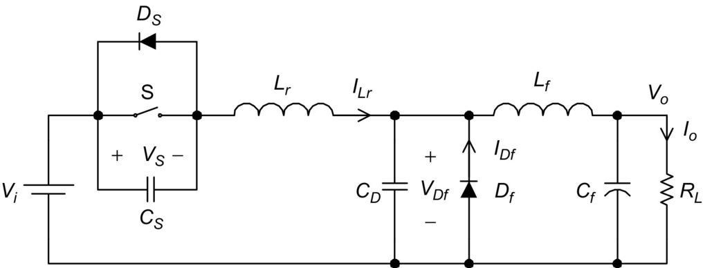

Instead of having one resonant stage, there are three in this converter. The mode I operation in Fig. 12.16A is described first. Before the switch S is turned on, the output diode Df is conducting, and the resonant inductor current ILr is negative (flowing through the antiparallel diode of S). S is then turned on with ZVS. The resonant inductor current ILr increases linearly and Df is still conducting. When ILr reaches the output current Io, the first resonant stage starts. The resonant circuit is formed by the resonant inductor Lr and the capacitor CD across the output diode. This stage ends when S is turned off with ZVS. Then, a second resonant stage starts. The resonant circuit consists of Lr, CD, and the capacitor across the switch Cs. This stage ends when the output diode becomes forward-biased. A third resonant stage will then start. Lr and Cs form the resonant circuit. This stage ends and completes one operation cycle when the diode Cs becomes forward-biased.
The only difference between mode I and mode II in Fig. 12.16B is in the third resonant stage, in which the resonant circuit is formed by Lr and CD. This stage ends when Df becomes forward-biased. The concept of the multiresonant switch can be applied to conventional converters [19–21]. A family of multi-resonant converters (MRCs) are shown in Fig. 12.17.

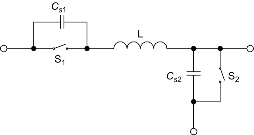
Although the variation of the switching frequency for regulation in MRCs is smaller than that of QRCs, a wideband frequency modulation is still required. Hence, the optimal design of magnetic components and the EMI filters in MRCs is not easy. It would be desirable to have a constant switching frequency operation. In order to operate the MRCs with constant switching frequency, the diode in Fig. 12.14 can be replaced with an active switch S2 [22]. A constant-frequency multiresonant (CF-MR) switch is shown in Fig. 12.18. The output voltage is regulated by controlling the on-time of the two switches. This concept can be illustrated with the buck converter as shown in Fig. 12.19, together with the gate drive waveforms and operating stages. S1 and S2 are turned on during the time when currents flow through the anti-parallel diodes of S1 and S2. This stage ends when S2 is turned off with ZVS. The first resonant stage is then started. Lr and CS2 form the resonant circuit. A second resonant stage begins. Lr resonates with CS1 and CS2. The voltage across S1 oscillates to zero. When ILr becomes negative, S1 will be turned on with ZVS. Then, Lr resonates with CS2. S2 will be turned on when current flows through DS2. As the output voltage is the average voltage across S2, output voltage regulation is achieved by controlling the conduction time of S2.

All switches in MRCs operate with ZVS, which reduces the switching losses and switching noise and eliminates the oscillation due to the parasitic effects of the components (such as the junction capacitance of the diodes). However, all switches are under high current and voltage stresses, resulting in an increase in the conduction loss.
12.7 Zero-voltage-transition Converters
By introducing a resonant circuit in parallel with the switches, the converter can achieve ZVS for both power switch and diode without significantly increasing their voltage and current stresses [23]. Fig. 12.20A shows a buck-type ZVT-PWM converter, and Fig. 12.20B shows the associated waveforms. The converter consists of a main switch S and an auxiliary switch S1. It can be seen that the voltage and current waveforms of the switches are square-wave-like except during turn-on and turn-off switching intervals, where zero-voltage-transition (ZVT) takes place. The main switch and the output diode are under ZVS and are subjected to low voltage and current stresses. The auxiliary switch is under ZCS, resulting in low switching loss.

The concept of ZVT can be extended to other PWM circuits by adding the resonant circuit. Some basic ZVT-PWM converters are shown in Fig. 12.21.

12.8 Non-dissipative Active Clamp Network
The active-clamp circuit can utilize the transformer leakage inductance energy and can minimize the turn-off voltage stress in the isolated converters. The active-clamp circuit provides a means of achieving ZVS for the power switch and reducing the rate of change of the diode's reverse-recovery current. An example of a flyback converter with active clamp is shown in Fig. 12.22A, and the circuit waveforms are shown in Fig. 12.22B. Clamping action is obtained by using a series combination of an active switch (i.e., S2) and a large capacitor so that the voltage across the main switch (i.e., S1) is clamped to a minimum value. S2 is turned on with ZVS. However, S2 is turned off with finite voltage and current and has turn-off switching loss. The clamp-mode ZVS-MRCs is discussed in [24–26].

12.9 Load Resonant Converters
Load resonant converters (LRCs) have many distinct features over conventional power converters. Due to the soft commutation of the switches, no turn-off loss or stress is present. LRCs are especially suitable for high-power applications because they allow high-frequency operation for equipment size/weight reduction, without sacrificing the conversion efficiency and imposing extra stress on the switches. Basically, LRCs can be divided into three different configurations, namely, series resonant converters, parallel resonant converters, and series-parallel resonant converters.
12.9.1 Series Resonant Converters
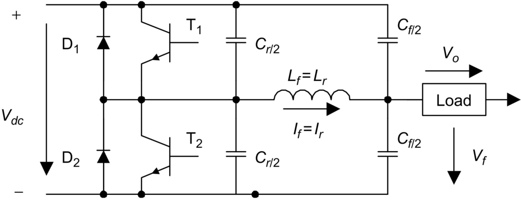
Series resonant converters (SRCs) have their load connected in series with the resonant tank circuit, which is formed by Lr and Cr [15,27–29]. The half-bridge configuration is shown in Fig. 12.23. When the resonant inductor current iLr is positive, it flows through T1 if T1 is on; otherwise, it flows through the diode D2. When iLr is negative, it flows through T2 if T2 is on; otherwise, it flows through the diode D1. In the steady-state symmetrical operation, both the active switches are operated in a complementary manner. Depending on the ratio between the switching frequency ωS and the converter resonant frequency ωr, the converter has several possible operating modes.

12.9.1.1 Discontinuous Conduction Mode With ωS<0.5ωr
Fig. 12.24A shows the waveforms of iLr and the resonant capacitor voltage vCr in this mode of operation. From 0 to t1, T1 conducts. From t1 to t2, the current in T1 reverses its direction. The current flows through D1 and back to the supply source. From t2 to t3, all switches are in the off state. From t3 to t4, T2 conducts. From t4 to t5, the current in T2 reverses its direction. The current flows through D2 and back to the supply source. T1 and T2 are switched on under ZCS condition, and they are switched off under zero-current and zero-voltage conditions. However, the switches are under high current stress in this mode of operation and thus have higher conduction loss.
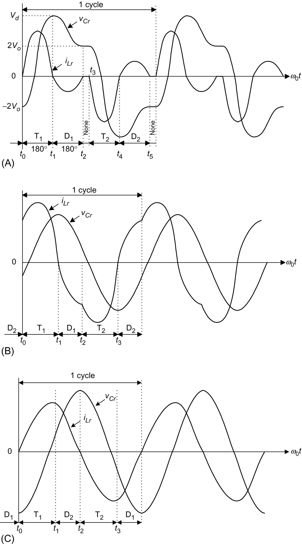
12.9.1.2 Continuous Conduction Mode With 0.5ωr<ωS<ωr
Fig. 12.24B shows the circuit waveforms. From 0 to t1, iLr transfers from D2 to T1. T1 is switched on with finite switch current and voltage, resulting in turn-on switching loss. Moreover, the diodes must have good reverse-recovery characteristics in order to reduce the reverse-recovery current. From t1 to t2, D1 conducts and T1 is turned off softly with zero voltage and zero current. From t2 to t3, T2 is switched on with finite switch current and voltage. At t3, T2 is turned off softly and D2 conducts until t4.
12.9.1.3 Continuous Conduction Mode With ωr<ωS
Fig. 12.24C shows the circuit waveforms. From 0 to t1, iLr transfers from D1 to T1. Thus, T1 is switched on with zero current and zero voltage. At t1, T1 is switched off with finite voltage and current, resulting in turn-off switching loss. From t1 to t2, D2 conducts. From t2 to t3, T2 is switched on with zero current and zero voltage. At t3, T2 is switched off. iLr transfers from T2 to D1. As the switches are turned on with ZVS, lossless snubber capacitors can be added across the switches.
The following parameters are defined: voltage conversion ratio M, characteristic impedance Zr, resonant frequency fr, normalized load resistance r, normalized switching frequency γ.
The relationships between M and γ for different value of r are shown in Fig. 12.25. The boundary between continuous conduction mode (CCM) and discontinuous conduction mode (DCM) is at r=1.27γ. When the converter is operating in DCM and 0.2<γ<0.5, M=1.27rγ.

The SRC has the following advantages. Transformer saturation can be avoided since the series capacitor can block the DC component. The light-load efficiency is high because the device current and conduction loss are low. However, the major disadvantages are that there is difficulty in regulating the output voltage under light-load and no-load conditions. Moreover, the output DC filter capacitor has to carry high ripple current, which could be a major problem in low-output-voltage and high-output-current applications [29].
12.9.2 Parallel Resonant Converters
Parallel resonant converters (PRCs) have their load connected in parallel with the resonant tank capacitor Cr [27–30]. The half-bridge configuration is shown in Fig. 12.26. SRC behaves as a current source, whereas the PRC acts as a voltage source. For voltage regulation, PRC requires a smaller operating frequency range than the SRC to compensate for load variation.

12.9.2.1 Discontinuous Conduction Mode
The steady-state waveforms of the resonant inductor current iLr and the resonant capacitor voltage vCr are shown in Fig. 12.27A. Initially, both iLr and vCr are zero. From 0 to t2, T1 conducts and is turned on with zero current. When iLr is less than the output current Io, iLr increases linearly from 0 to t1 and the output current circulates through the diode bridge. From t1 to t3, Lr resonates with Cr. Starting from t2, iLr reverses its direction and flows through D1. T1 is then turned off with zero current and zero voltage. From t3 to t4, vCr decreases linearly due to the relatively constant value of Io. At t4, when vCr equals zero, the output current circulates through the diode bridge again. Both iLr and vCr will stay at zero for an interval. From t5 to t9, the above operations will be repeated for T2 and D2. The output voltage is controlled by adjusting the time interval of [t4, t5].
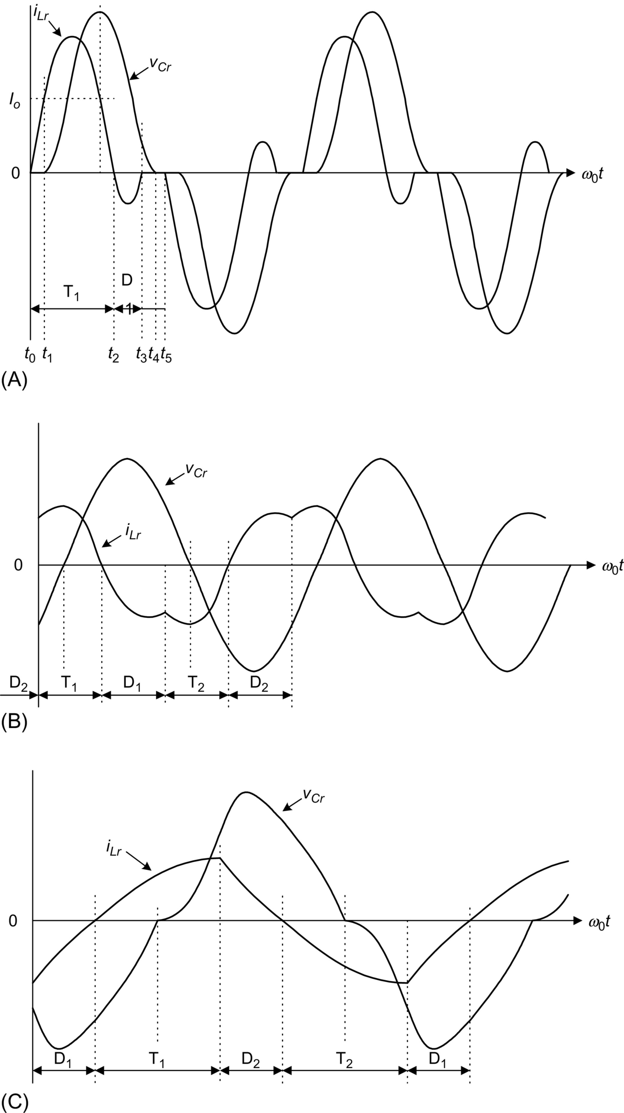
12.9.2.2 Continuous Conduction Mode ωS<ωr
This mode is similar to the operation in the DCM but with a higher switching frequency. Both iLr and vCr become continuous. The waveforms are shown in Fig. 12.27B. The switches T1 and T2 are hard turned on with finite voltage and current and are soft turned off with ZVS.
12.9.2.3 Continuous Conduction Mode ωS>ωr
If the switching frequency is higher than ωr (Fig. 12.27C), the antiparallel diode of the switch will be turned on before the switch is triggered. Thus, the switches are turned on with ZVS. However, the switches are hard turned off with finite current and voltage.
The parameters defined in Eq. (12.2) are applicable. The relationships between M and γ for various values of r are shown in Fig. 12.28. During the DCM (i.e., γ<0.5), M is in linear relationship with γ. Output voltage regulation can be achieved easily. The output voltage is independent on the output current. The converter shows good voltage-source characteristics. It is also possible to step up and step down the input voltage.

The PRC has the advantages that the load can be short-circuited and the circuit is suitable for low-output-voltage, high-output-current applications. However, the major disadvantage of the PRC is the high device current. Moreover, since the device current does not decrease with the load, the efficiency drops with a decrease in the load [29].
12.9.3 Series-Parallel Resonant Converter
Series-parallel resonant converter (SPRC) combines the advantages of the SRC and PRC. The SPRC has an additional capacitor or inductor connected in the resonant tank circuit [29–31]. Fig. 12.29A shows an LCC-type SPRC, in which an additional capacitor is placed in series with the resonant inductor. Fig. 12.29B shows an LLC-type SPRC, in which an additional inductor is connected in parallel with the resonant capacitor in the SRC. However, there are many possible combinations of the resonant tank circuit. Detailed analysis can be found in [31].
12.10 Control Circuits for Resonant Converters
Since the 1985s, various control integrated circuits (ICs) for resonant converters have been developed. Some common ICs for different converters are described in this section.
12.10.1 QRCs and MRCs
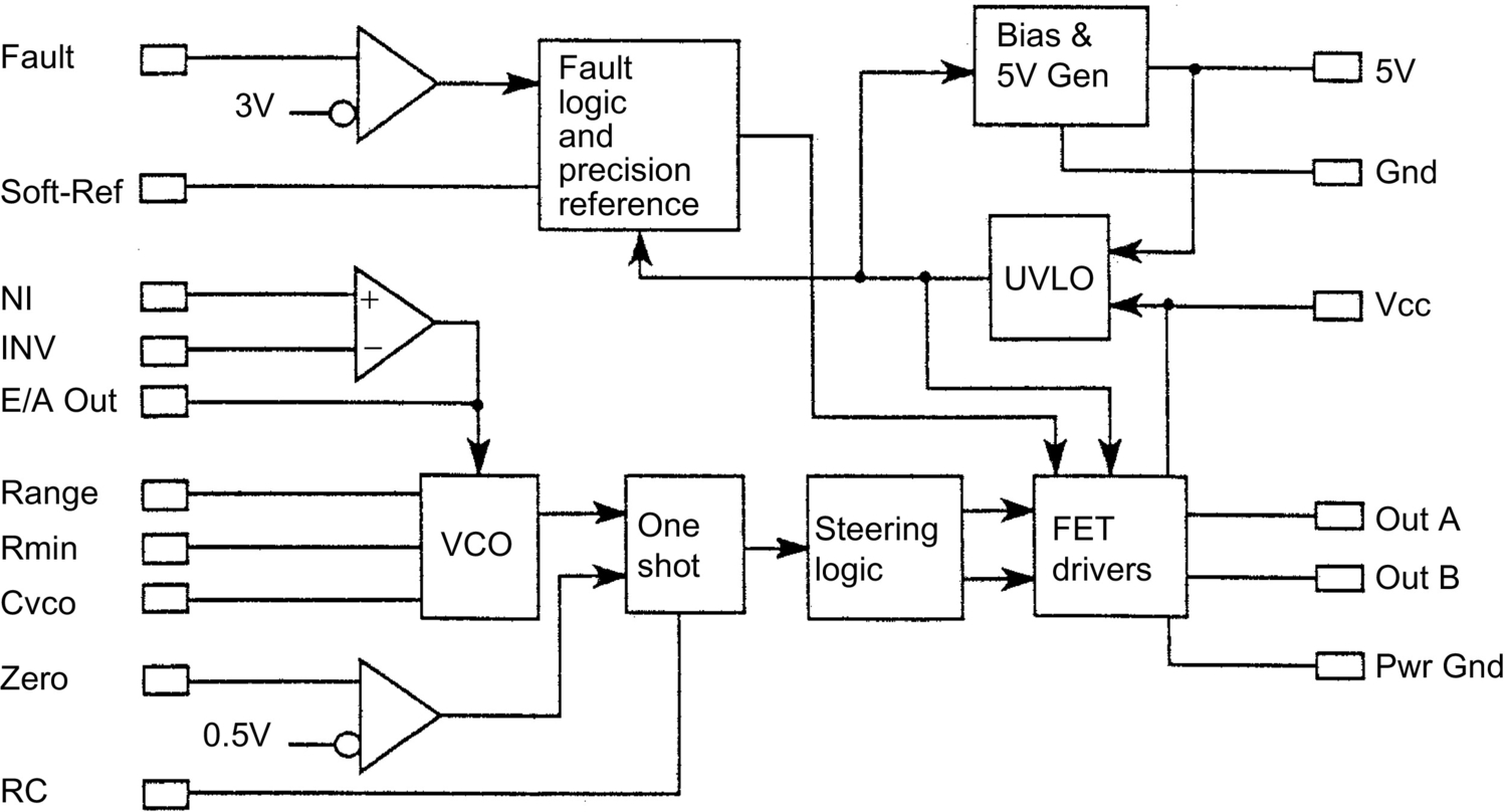
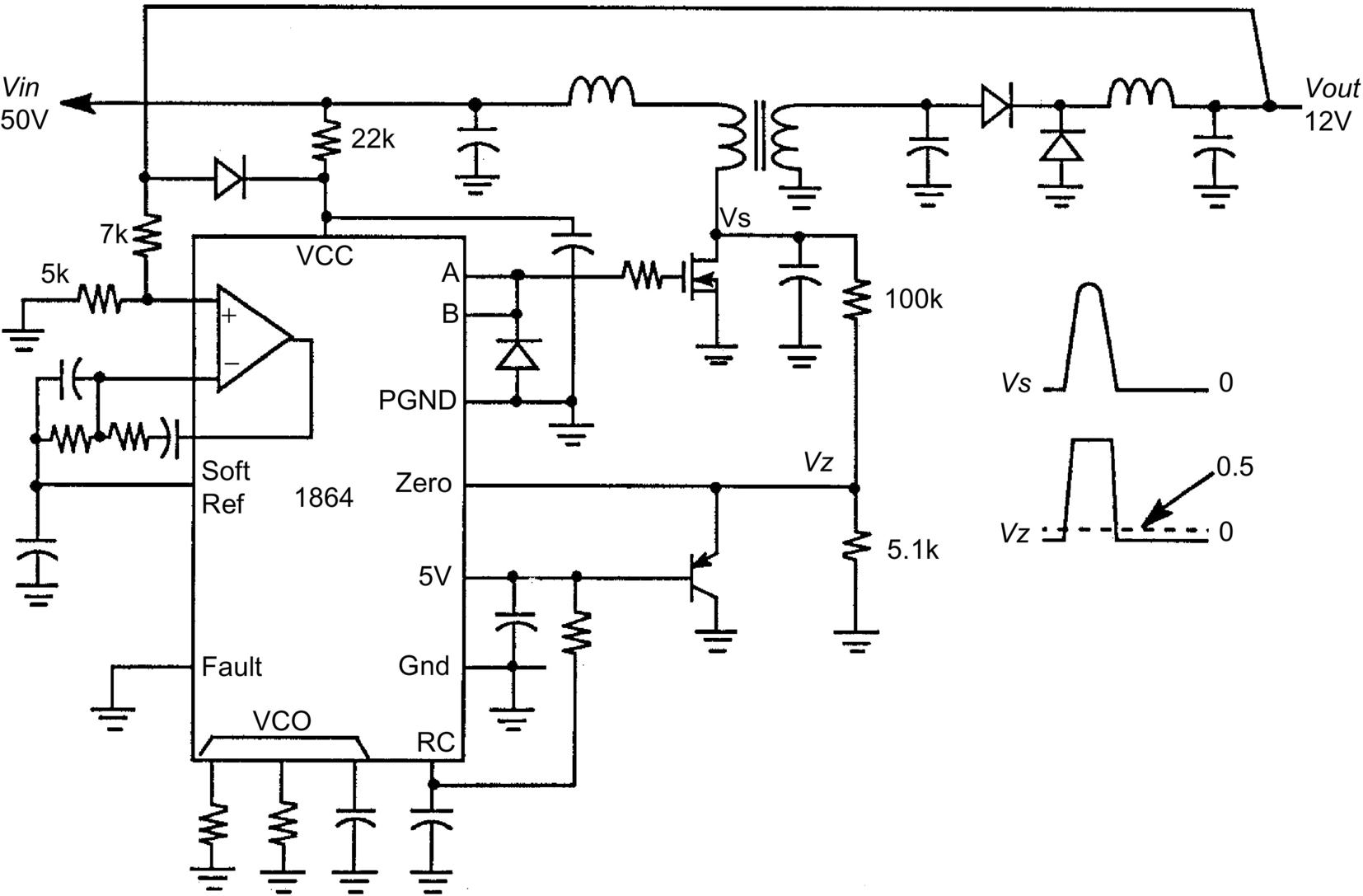
Output regulations in many resonant-type converters, such as QRCs and MRCs, are achieved by controlling the switching frequency. ZCS applications require controlled switch-on times, while ZVS applications require controlled switch-off times. The fundamental control blocks in the IC include an error amplifier, voltage-controlled oscillator (VCO), one-shot generator with a zero wave-crossing detection comparator, and an output stage to drive the active switch. Typical ICs include UC1861-UC1864 for ZVS applications and UC 1865-UC 1868 for ZCS applications [32]. Fig. 12.30 shows the controller block diagram of UC 1864.
The maximum and minimum switching frequencies (i.e., fmax and fmin) are controlled by the resistors Range and Rmin and the capacitor Cvco. fmax and fmin can be expressed as

The frequency range Δf is then equal to

The frequency range of the ICs is from 10 kHz to 1 MHz. The output frequency of the oscillator is controlled by the error amplifier (E/A) output. An example of a ZVS-MR forward converter is shown in Fig. 12.31.
12.10.2 Phase-shifted, ZVT FB Circuit
The UCC3895 is a phase-shift PWM controller that can generate a phase-shifting pattern of one half-bridge with respect to the other. The application diagram is shown in Fig. 12.32.
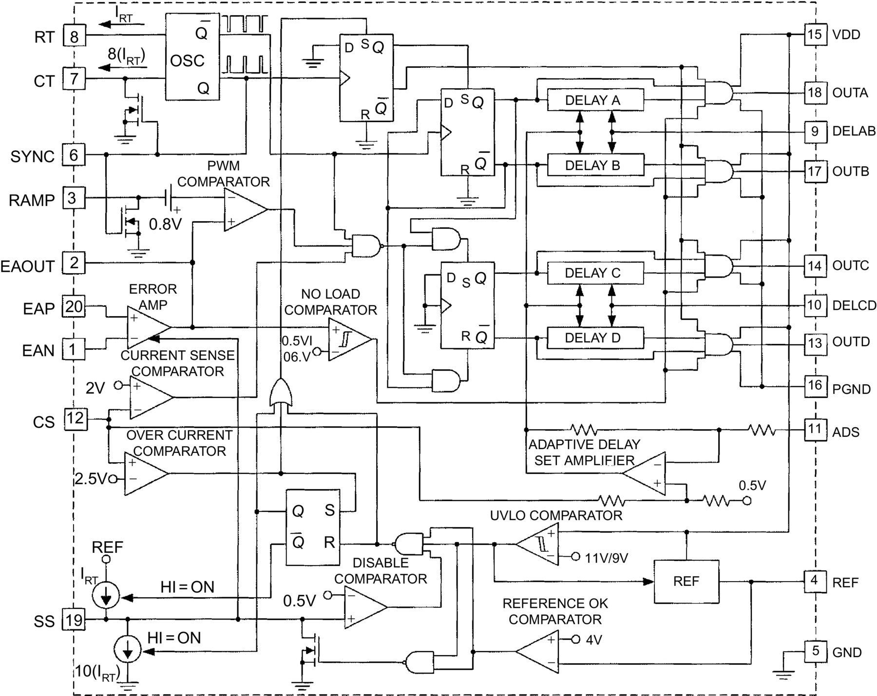
The four outputs “OUTA,” “OUTB,” “OUTC,” and “OUTD” are used to drive the MOSFETs in the full-bridge. The dead time between “OUTA” and “OUTB” is controlled by “DELAB,” and the dead time between “OUTC” and “OUTD” is controlled by “DELCD.” Separate delays are provided for the two half-bridges to accommodate differences in resonant capacitor charging currents. The delay in each set is approximated by

where RDEL is the resistor value connected between “DELAB” and “DELCD” to ground.
The oscillator period is determined by RT and CT. It is defined as

The maximum operating frequency is 1 MHz. The phase shift between the two sets of signals is controlled by the ramp voltage and the error amplifier output having a 7-MHz bandwidth.
12.11 Extended-Period Quasi-Resonant Converters
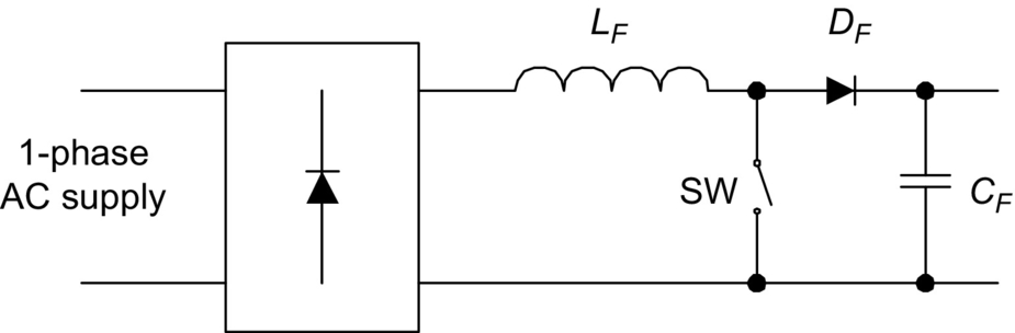
Generally, resonant and quasi-resonant converters operate with frequency control. The extended-period quasi-resonant (EP-QR) converters proposed by Barbi [33] offer a simple solution to modify existing hard-switched converters into soft-switched ones with constant frequency operation. This makes both output filter design and control simple. Fig. 12.33 shows a standard hard-switched boost-type PFC converter. In this hard-switched circuit, the main switch SW1 could be subject to significant switching stress because the reverse-recovery current of the diode DF could be excessive when SW1 is turned on. In practice, a small saturable inductor may be added in series with the power diode DF in order to reduce the di/dt of the reverse-recovery current. In addition, an optional R-C snubber may be added across SW1 to reduce the dv/dt of SW1. These extra reactance components can in fact be used in the EP-QR circuit to achieve soft switching, as shown in Fig. 12.34. The resonant components Lr and Cr are of small values and can come from the snubber circuits of a standard hard-switched converter. Thus, the only additional component is the auxiliary switch Q2. The small resonant inductor is put in series with the main switch SW1 so that SW1 can be switched on under ZC condition and the di/dt problem of the reverse-recovery current be eliminated. The resonant capacitor Cr is used to store energy for creating condition for soft switching. Q2 is used to control the resonance during the main switch transition. It should be noted that all power devices including SW1, Q1, and main power diode DF are turned on and off under ZV and/or ZC conditions. Therefore, the large di/dt problem due to the reverse recovery of the power diode can be eliminated. The soft-switching method is an effective technique for EMI suppression.

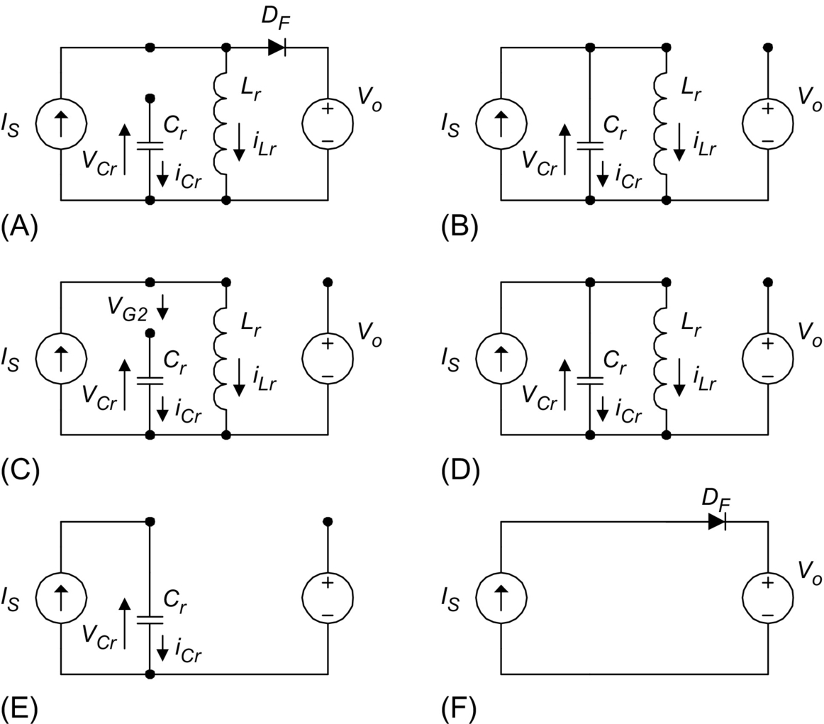
Together with power factor correction technique, soft-switching converters offer a complete solution to meet EMI regulations for both conducted and radiated EMI. The operation of the EP-QR boost PFC circuit [34,35] can be described in six modes as shown in Fig. 12.35. The corresponding idealized waveforms are included in Fig. 12.36.

12.11.0.1 Circuit Operation
Interval I: (t0−t1). Due to the resonant inductor Lr limits the di/dt of the switch current, switch SW1 is turned on at zero-current condition with a positive gating signal VGS1 to start a switching cycle at t=t0. Current in DF is diverted to inductor Lr. Because DF is still conducting during this short period, DS2 is still reverse-biased and is thus not conducting. The equivalent circuit topology for the conducting paths is shown in Fig. 12.35A. Resonant switch Q2 remains off in this interval.
Interval II: (t1−ta). When DF regains its blocking state, DS2 becomes forward-biased. The first half of the resonance cycle occurs and resonant capacitor Cr starts to discharge, and current flows in the loop Cr-Q2-Lr-SW1. The resonance half cycle stops at time t=ta because DS2 prevents the loop current iCr from flowing in the opposition direction. The voltage across Cr is reversed at the end of this interval. The equivalent circuit is shown in Fig. 12.35B.
Interval III: (ta−tb). Between ta and tb, current in LF and Lr continues to build up. This interval is the extended period for the resonance during which energy is pumped into Lr. The corresponding equivalent circuit is shown in Fig. 12.35C.
Interval IV: (tb−t2). Fig. 12.35D shows the equivalent circuit for this operating mode. Before SW1 is turned off, the second half of the resonant cycle needs to take place in order that a zero-voltage condition can be created for the turn-off process of SW1. The second half of the resonant cycle starts when auxiliary switch Q2 is turned on at t=tb. Resonant current then flows through the loop Lr-Q2-Cr-antiparallel diode of SW1. This current is limited by Lr, and thus, Q2 is turned on under zero-current condition. Since the antiparallel diode of SW1 is conducting, the voltage across SW1 is clamped to the on-state voltage of the antiparallel diode. SW1 can therefore be turned off at (near) zero-voltage condition before t=t2 at which the second half of the resonant cycle ends.
Interval V: (t2−t3). During this interval, the voltage across Cr is less than the output voltage Vo. Therefore, DF is still reverse-biased. Inductor current Is flows into Cr until VCr reaches Vo at t=t3. The equivalent circuit is represented in Fig. 12.35E.
Interval VI: (t3−t4). During this period, the resonant circuit is not in action, and the inductor current Is charges the output capacitor CF via DF, as in the case of a classical boost-type PFC circuit. Cr is charged to Vo; therefore, Q2 can be turned off at zero-voltage and zero-current conditions. Fig. 12.35F shows the equivalent topology of this operating mode.
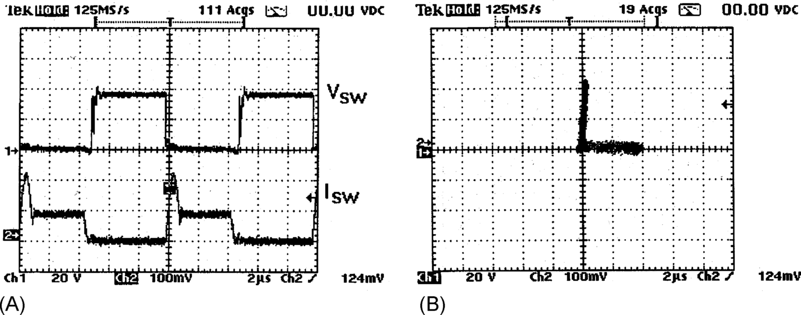
In summary, SW1, Q2, and DF are fully soft-switched. Since the two resonance half cycles take place within a closed loop outside the main inductor, the high resonant pulse will not occur in the inductor current, thus making a well-established averaged current mode control technique applicable for such QR circuit. For full soft switching in the turn-off process, the resonant components need to be designed so that the peak resonant current exceeds the maximum value of the inductor current. Typical measured switching waveforms and trajectories of SW1, Q2, and DF are shown in Figs. 12.37, 12.38, and 12.39, respectively.


12.11.0.2 Design Procedure
Given: Input AC voltage=Vs (V)
Peak AC voltage=Vs(max) (V)
Nominal output DC voltage=Vo (V)
Switching frequency=fsw (Hz)
Output power=Po (W)
Input current ripple=ΔI (A)
Output voltage ripple=ΔV (V)
(I) Resonant tank design:
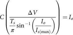
Step 1. Because the peak resonant current must be greater than the peak inductor current (same as peak input line current) in order to achieve soft turnoff, it is necessary to determine the peak input current Is(max). Assuming lossless AC-DC power conversion, Is(max) can be estimated from the following equation:

where Io=Po/Vo is the maximum output current.
Step 2. Soft-switching criterion is

where ![]() is the impedance of the resonant tank.
is the impedance of the resonant tank.
For a chosen resonant, frequency fr, Lr, and Cr can be obtained from

(II) Filter component design:
The minimum conversion ratio is
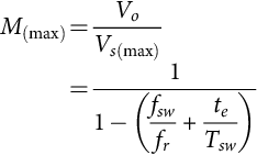
where Tsw=1/fsw and te is the extended period. From Eq. (12.10), minimum te can be estimated.
The turn-on period of the SW1 is
Inductor value L is obtained from

The filter capacitor value C can be determined from
where Ts=1/fs is the period of the AC voltage supply frequency.
12.11.1 Soft-Switched DC-DC Flyback Converter
A simple approach that can turn an existing hard-switched converter design into a soft-switched one is shown in Fig. 12.40. The key advantage of the proposal is that many well proved and reliable hard-switched converter designs can be kept. The modification required is the addition of a simple circuit (consisting an auxiliary winding, a switch, and a small capacitor) to an existing isolated converter [36]. This principle, which is the modified version of the EPQR technique for isolated converter, is demonstrated in an isolated soft-switched flyback converter with multiple outputs. Other advantageous features of the proposal are as follows:
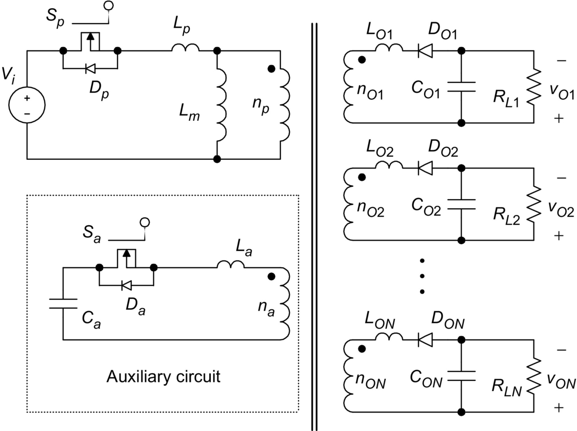
• All switches and diodes of the converter are “fully” soft-switched, that is, soft-switched at both turn-on and turn-off transitions under zero-voltage and/or zero-current conditions.
• The leakage inductance of each winding in the flyback transformer forms part of the resonant circuit for achieving ZVS and ZCS of all switches and diodes.
• The control technique is simply PWM-based as in standard hard-switched converters.
• The soft-switched technique is a proved method for EMI reduction [37].
12.11.2 A ZCS Bidirectional Flyback DC-DC Converter
A bidirectional flyback DC-DC converter that uses one auxiliary circuit for both power flow directions is proposed in Fig. 12.41 [38]. The methodology is based on extending the unidirectional soft-switched flyback converter in Ref. [36] and replacing the output diode with a controlled switch, which acts as either a rectifier [39] or a power control switch in the corresponding power flow direction. An auxiliary circuit that consists of a winding in the coupled inductor, a switch, and a capacitor converts the hard-switched design into a soft-switched one. The operation is the same as [36] in the forward mode. An extended-period resonant stage [34] is introduced when the power control switch is on. Conversely, in the reverse mode, a complete resonant stage is initiated before the main switch is off. In both the power flow operations, the leakage inductance of the coupled inductor is used to create zero-current switching conditions for all switches.

12.12 Soft-Switching and EMI Suppression
A family of EP-QR converters are displayed in Fig. 12.42. Their radiated EMI emissions have been compared with that from their hard-switched counterparts [37]. Fig. 12.43A and B shows the conducted EMI emission from a hard-switched flyback converter and a soft-switched one, respectively. Their radiated EMI emissions are included in Fig. 12.44. Both converters are tested at an output power of 50 W. No special filtering or shielding measures have been taken during the measurement. It is clear from the measurements that soft switching is an effective means to EMI suppression.


12.13 Snubbers and Soft-Switching for High Power Devices
Today, most of the medium power (up to 200 kVA) and medium voltage (up to 800 V) inverter are hard-switched. Compared with low-power switched-mode power supplies, the high voltage involved in the power inverters makes the dv/dt, di/dt, and the switching stress problems more serious. In addition, the reverse recovery of power diodes in the inverter leg may cause very sharp current spike, leading to severe EMI problem. It should be noted that some high-power devices such as GTO thyristors do not have a square safe operating area (SOA). It is therefore essential that the switching stress they undergone must be within their limits. Commonly used protective measures are to use snubber circuits for protecting high-power devices.
Among various snubbers, two snubber circuits are most well-known for applications in power inverters. They are the Undeland snubber [40] (Fig. 12.45) and McMurray snubber circuits [41] (Fig. 12.46). The Undeland snubber is an asymmetrical snubber circuit with one turn-on inductor and one turn-off capacitor. The turn-off snubber capacitor Cs is clamped by another capacitor Cc. At the end of each switching cycle, the snubber energy is dumped into Cc and then discharged into the DC bus via a discharge resistor. In order to reduce the snubber loss, the discharge resistor can be replaced by a switched-mode circuit. In this way, the Undeland snubber can become a snubber with energy recovery. The McMurray snubber is symmetrical. Both the turn-off snubber capacitors share current in parallel during turnoff. The voltage transient is limited by the capacitor closest to the turn-off device because the stray inductance to the other capacitor will prevent instantaneous current sharing. The turn-on inductors require midpoint connection. Snubber energy is dissipated into the snubber resistor. Like the Undeland snubber, the McMurray snubber can be modified into an energy recovery snubber. By using an energy recovery transformer as shown in Fig. 12.47, this snubber becomes a regenerative one. Although other regenerative circuits have been proposed, their complexity makes them unattractive in industrial applications. Also, they do not necessarily solve the power diode reverse-recovery problems.


Although the use of snubber circuits can reduce the switching stress in the power devices, the switching loss is actually damped into the snubber resistors unless regenerative snubbers are used. The switching loss is still a limiting factor to the high-frequency operation of power inverters. However, the advent of soft-switching techniques opens a new way to high-frequency inverter operation. Because the switching trajectory of a soft-switched switch is close to the voltage and current axis, faster power electronic devices with smaller SOAs can in principle be used. In general, both ZVS and ZCS can reduce switching loss in high-power power switches. However, for power switches with tail currents, such as IGBT, ZCS is more effective than ZVS.
12.14 Soft-Switching DC-AC Power Inverters
Soft-switching technique not only offers a reduction in switching loss and thermal requirement but also allows the possibility of high-frequency and snubberless operation. Improved circuit performance and efficiency and reduction of EMI emission can be achieved. For zero-voltage switching (ZVS) inverter applications, two major approaches that enable inverters to be soft-switched have been proposed. The first approach pulls the DC link voltage to zero momentarily so that the inverter's switches can be turned on and off with ZVS. Resonant DC link and quasi-resonant inverters belong to this category. The second approach uses the resonant pole idea. By incorporating the filter components into the inverter operation, resonance condition and thus zero-voltage/current conditions can be created for the inverter switches.
In this section, the following soft-switched inverters are described:
Approach 1: Resonant DC link inverters are as follows:
1. Resonant (pulsating) DC link inverters
2. Actively clamped resonant DC link inverters
3. Resonant inverters with minimum voltage stress
4. Quasi-resonant soft-switched inverter
5. Parallel resonant DC link inverter
Approach 2: Resonant pole inverters (RPIs) are as follows:
2. Auxiliary RPIs
3. Auxiliary resonant commutated pole inverters (ARCPIs)
Type 1 is the resonant DC link inverter [42–44] that sets the DC link voltage into oscillation so that the zero-voltage instants are created periodically for ZVS. Despite the potential advantages that this soft-switching approach can offer, a recent review on existing resonant-link topologies for inverters [45] concludes that the resonant DC link system results in an increase in circuit complexity and the frequency spectrum is restricted by the need of using integral pulse-density modulation (IPDM) when compared with a standard hard-switched inverter. In addition, the peak pulsating link voltage of resonant-link inverters is twice the DC link voltage in a standard hard-switched inverter. Although clamp circuits (type 2) can be used to limit the peak voltage to 1.3–1.5 per unit [44], power devices with higher than normal voltage ratings have to be used.
Circuits of types 3–5 employ a switched-mode front-stage circuit that pulls the DC link voltage to zero momentarily whenever inverter switching is required. This soft-switching approach does not cause extra voltage stress to the inverter, and hence, the voltage rating of the power devices is only 1 per unit. As ZVS conditions can be created at any time, there is virtually no restriction in the PWM strategies. Therefore, well-established PWM schemes developed in the last 2 decades can be employed. In some ways, this approach is similar to some DC-side commutation techniques proposed in the past for thyristor inverters [46,47], although these DC-side commutation techniques were used for turning off thyristors in the inverter bridge and were not primarily developed for soft switching.
Circuits of type 6–8 retain the use of a constant DC link voltage. They incorporate the use of the resonant components and/or filter components into the inverter circuit operation. This approach is particularly useful for inverter applications in which output filters are required. Examples include uninterruptible power supplies (UPS) and inverters with output filters for motor drives. The LC filter components can form the auxiliary resonant circuits that create the soft-switching conditions. However, these tend to have high-power device count and require complex control strategy.
12.14.1 Resonant (Pulsating) DC Link Inverter
Resonant DC link converter for DC-AC power conversion was proposed in 1986 [42]. Instead of using a nominally constant DC link voltage, a resonant circuit is added to cause the DC link voltage to be pulsating at a high frequency. This resonant circuit theoretically creates periodic zero-voltage duration at which the inverter switches can be turned on or off. Fig. 12.48 shows the schematics of the pulsating link inverter. Typical DC link voltage, inverter's phase voltage, and the line voltages are shown in Fig. 12.49. Because the inverter switching can only occur at zero-voltage duration, integral pulse-density modulation (IPDM) has to be adopted in the switching strategy.

Analysis of the resonant DC link converter can be simplified by considering that the inverter system is highly inductive. The equivalent circuit is shown in Fig. 12.50.

The link current Ix may vary with the changing load condition but can be considered constant during the short resonant cycle. If switch S is turned on when the inductor current is ILo, the resonant DC link voltage can be expressed as
and inductor current iL is
where
and
The resistance in the inductor could affect the resonant behavior because it dissipates some energy. In practice, (iL−Ix) has to be monitored when S is conducting. S can be turned on when (iL−Ix) is equal to a desired value. The objective is to ensure that the DC link voltage can be resonated to zero-voltage level in the next cycle.
The pulsating DC link inverter has the following advantages:
• Reduction of switching loss.
• Snubberless operation.
• High switching frequency (>18 kHz) operation becomes possible, leading to the reduction of acoustic noise in inverter equipment.
• Reduction of heat sink requirements and thus improvement of power density.
This approach has the following limitations:
• The peak DC pulsating link voltage (2.0 per unit) is higher than the nominal DC voltage value of a conventional inverter. This implies that power devices and circuit components of higher voltage ratings must be used. This could be a serious drawback because power components of higher voltage ratings not only are more expensive but also usually have inferior switching performance than their low-voltage counterparts.
• Although voltage clamp can be used to reduce the peak DC link voltage, the peak voltage value is still higher than normal, and the additional clamping circuit makes the control more complicated.
• Integral pulse-density modulation has to be used. Many well-established PWM techniques cannot be employed.
Despite these advantages, this resonant converter concept has paved the way for other soft-switched converters to develop.
12.14.2 Active-Clamp Resonant DC Link Inverter
In order to solve the high voltage requirement in the basic pulsating DC link inverters, active-clamping techniques (Fig. 12.51) have been proposed. The active clamp can reduce the per unit peak voltage from 2.0 to about 1.3–1.5 [44]. It has been reported that operating frequency in the range of 60–100 kHz has been achieved [48] with an energy efficiency of 97% for a 50 kVA drive system.
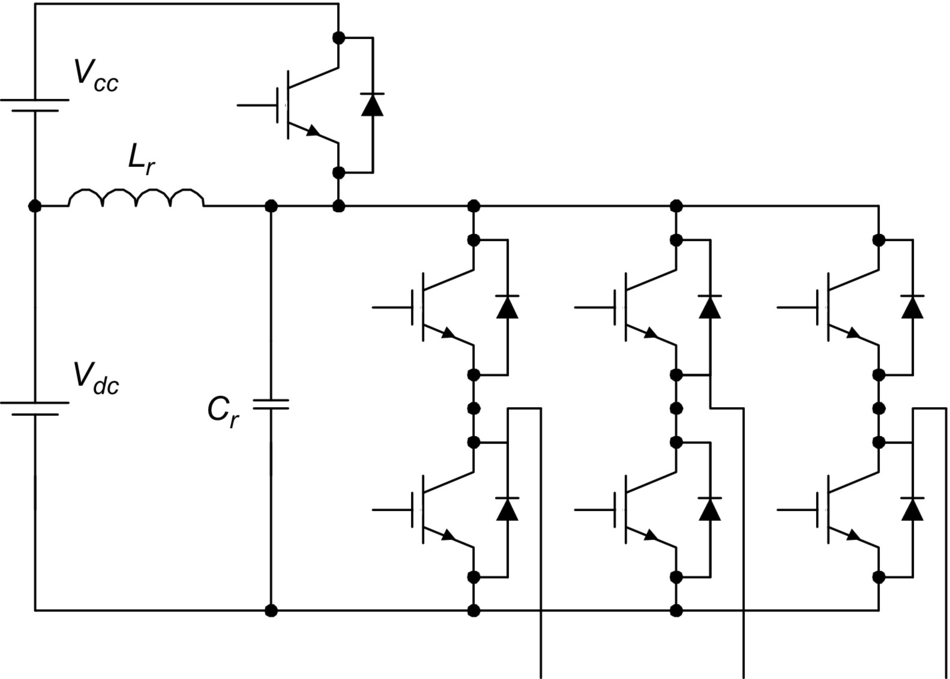
The design equations for active-clamp resonant-link inverter are

where TL is the minimum link period, fL is the maximum link frequency, and k is the clamping ratio. For the active-clamp resonant inverter, k is typically 1.3–1.4 per unit.
The rate of rise of the current in the clamping device is

The peak clamping current required to ensure that the DC bus return to 0 V is

In summary, resonant (pulsating) DC link inverters offer significant advantages such as the following:
• High switching frequency operation
• Low dv/dt for power devices
• ZVS with reduced switching loss
• Suitable for 1–250 kW
• Rugged operation with few failure mode
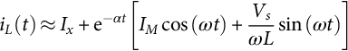
12.14.3 Resonant DC Link Inverter With Low Voltage Stress [49]
A resonant DC link inverter with low voltage stress is shown in Fig. 12.52. It consists of a front-end resonant converter that can pull the DC link voltage down just before any inverter switching. This resonant DC circuit serves as an interface between the DC power supply and the inverter. It essentially retains all the advantages of the resonant (pulsating) DC link inverters. But it offers extra advantages such as the following:

• No increase in the DC link voltage when compared with conventional hard-switched inverter. That is, the DC link voltage is 1.0 per unit.
• The zero-voltage condition can be created at any time. The ZVS is not restricted to the periodic zero-voltage instants as in resonant DC link inverter.
• Well-established PWM techniques can be employed.
• Power devices of standard voltage ratings can be used.
The timing program and the six operating modes of this resonant circuit are as shown in Figs. 12.53 and 12.54, respectively.

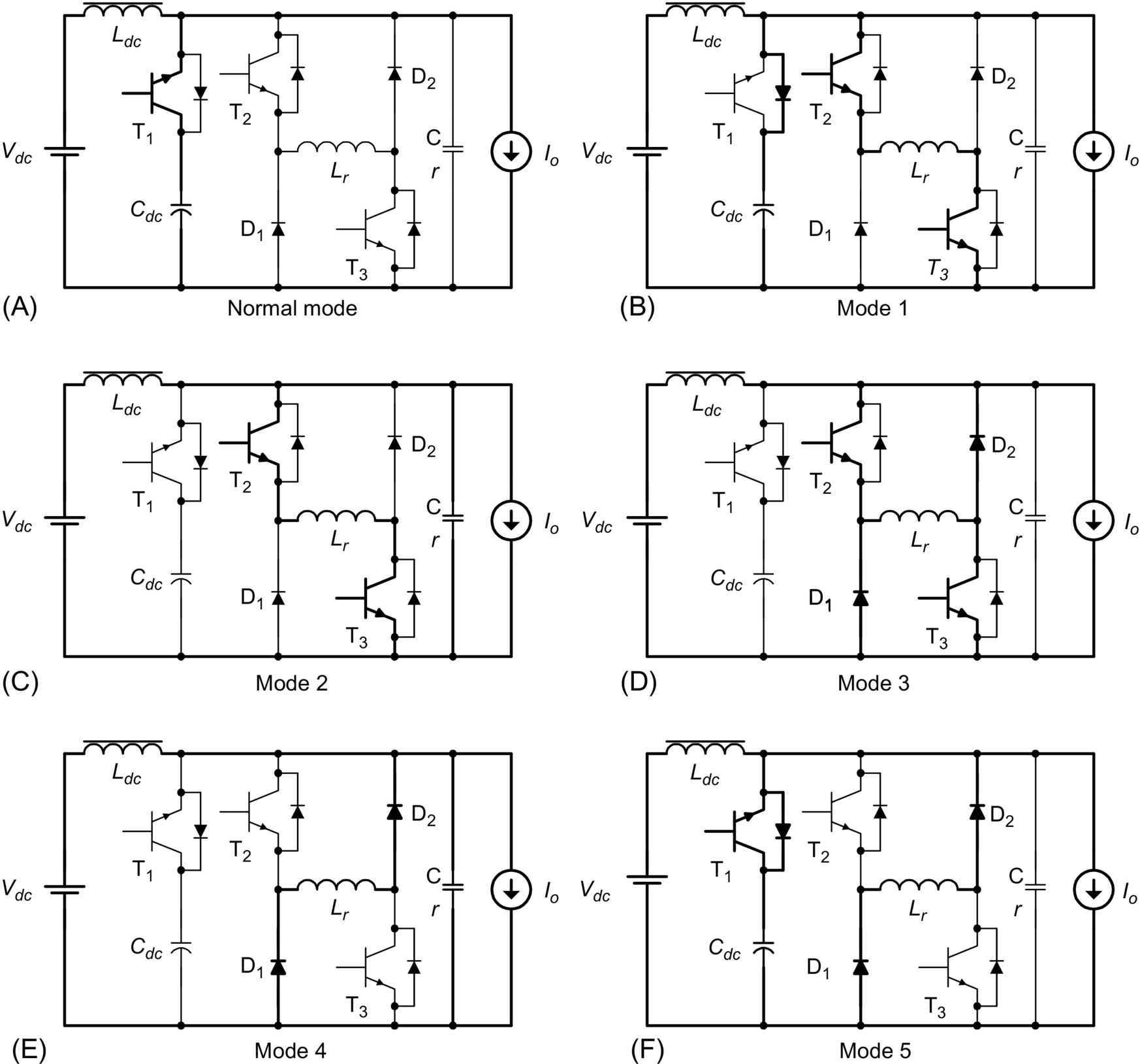
(1) Normal mode
This is the standard PWM inverter mode. The resonant inductor current iLr(t) and the resonant voltage Vcr(t) are given by
where Vs is the nominal DC link voltage.
(2) Mode 1 (Initiating mode): (t0−t1)
At t0, mode 1 begins by switching on T2 and T3 on with zero current. iLr(t) increases linearly with a di/dt of Vs/Lr. If iLr(t) is equal to the initialized current Ii, T1 is zero-voltage turned off. If (Is−Io)<Ii, then the initialization is ended when iLr (t) is equal to Ii, where Is is the current flowing into the DC inductor Ldc. If (Is−Io)>Ii, then this mode continues until iLr (t) is equal to (Is−Io). The equations in this interval are

(3) Mode 2 (Resonant mode): (t1−t2)
After T1 is turned off under ZVS condition, resonance between Lr and Cr occurs. Vcr (t) decreases from Vs to 0. At t2, iLr (t) reaches the peak value in this interval. The equations are
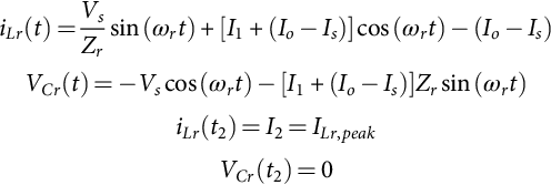
where

(4) Mode 3 (Freewheeling mode): (t2−t3)
The resonant inductor current flows through two freewheeling paths (T2-Lr-D2 and T3-D1-Lr). This duration is the zero-voltage period created for ZVS of the inverter and should be longer than the minimum on and off times of the inverter's power switches:
(5) Mode 4 (Resonant mode): (t3−t4)
This mode begins when T2 and T3 are switched off under ZVS. The second half of the resonance between Lr and Cr starts again. The capacitor voltage Vcr (t) increases back from 0 to Vs and is clamped to Vs. The relevant equations in this mode are
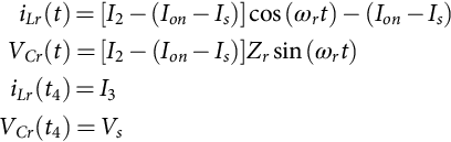
where Ion is the load current after the switching state.
(6) Mode 5 (Discharging mode): (t4−t5)
In this period, T1 is switched on under ZV condition because Vcr (t)=Vs. The inductor current decreases linearly. This mode finishes when iLr (t) becomes zero:

12.14.4 Quasi-Resonant Soft-Switched Inverter [50]
12.14.4.1 Circuit Operation
Consider an inverter fed by a DC voltage source versus a front-stage interface circuit shown in Fig. 12.55 can be added between the DC voltage source and the inverter. The front-stage circuit consists of a quasi-resonant circuit in which the first half of the resonance cycle is set to occur to create the zero-voltage condition whenever inverter switching is needed. After inverter switching has been completed, the second half of the resonance cycle takes place so that the DC link voltage is set back to its normal level. To avoid excessive losses in the resonant circuit, a small capacitor Cr1 is normally used to provide the DC link voltage, while the large smoothing DC link capacitor C1 is isolated from the resonant circuit just before the zero-voltage duration. This method avoids the requirement for pulling the DC voltage of the bulk capacitor to zero.
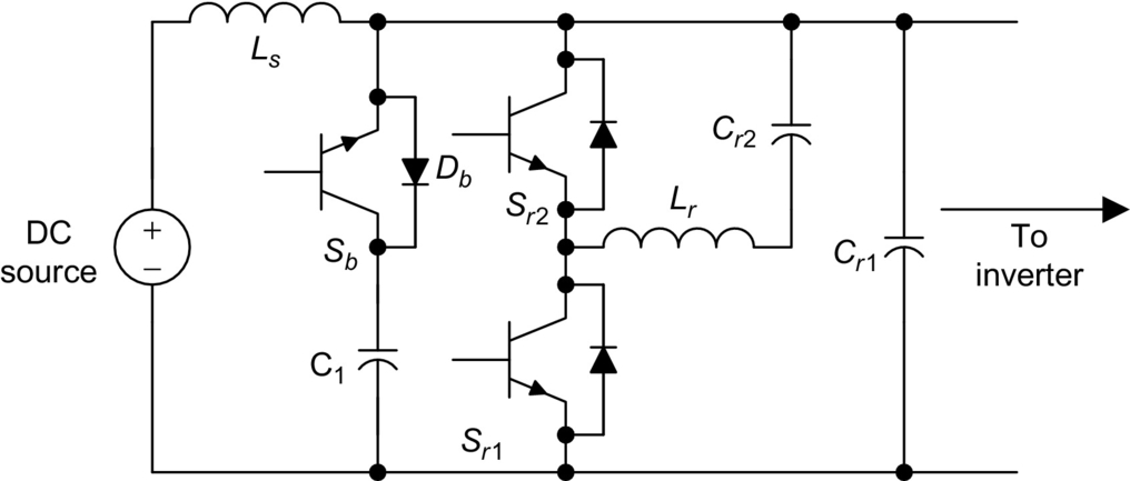
The period for this mode is from t0 to t1 in Fig. 12.56. In this mode, switch Sb is turned on, and switches Sr1 and Sr2 are turned off. The inverter in Fig. 12.55 works like a conventional DC link inverter. In this mode, Vcr1=Vc1. The voltage across switch Sb is zero. Before an inverter switching takes place, switch Sr1 is triggered at t1 to discharge Cr1. This operating mode ends at t2 when Vcr1 approaches zero. The equivalent circuit in this mode is shown in Fig. 12.57A. The switch Sb must be turned off at zero voltage when switch Sr1 is triggered. After Sr1 is triggered, Cr1 will be discharged via the loop Cr1, Cr2, Lr, and Sr1. Under conditions of Vcr2≤0 and Cr1≤Cr2, the energy stored in Cr1 will be transferred to Cr2, and Vcr1 falls to zero in the first half of the resonant cycle in the equivalent circuit of Fig. 12.57A. Vcr1 will be clamped to zero by the freewheel diodes in the inverter bridge and will not become negative. Thus, Vcr1 can be pulled down to zero for zero-voltage switching. When the current in inductor Lr becomes zero, switch Sr1 can be turned off at zero current.


Inverter switching can take place in the period from t2 to t3 in which Vcr1 remains zero. This period must be longer than the turn-on and turn-off times of the switches. When inverter switching has been completed, it is necessary to reset the voltage of capacitor Cr1. The equivalent circuit in this mode is shown in Fig. 12.57B. The current in inductor Lr reaches zero at t3. Due to the voltage in Vcr2 and the presence of diode Dr, this current then flows in the opposite direction. Cr1 will be recharged via Lr, Cr2, Cr1, and Dr. The diode Dr turns off when the current in Lr becomes zero. Vcr1 will not go beyond 1 per unit because Cr1 is clamped to supply voltage by diode Db. The switch Sb can be turned on again at zero-voltage condition when Vcr1 returns to normal DC supply voltage. After Dr turns off, Vcr2 may not be zero. Some positive residual capacitor voltage remains in C2 at t4, as shown in Fig. 12.56. In case Vcr2 is positive, Vcr1 cannot be pulled down to zero again in the next switching cycle. Therefore, Sr2 should be triggered after t4 to reverse the residual voltage in Cr2. At time t5, Sr2 turns off at zero-current condition, and Vcr2 is now reversed to negative. The equivalent circuit in this mode is shown in Fig. 12.57C. When Vcr2≤0 and Cr1≤Cr2, Vcr1 can be pulled down to zero again before the next inverter switching. The operation can then be repeated in next switching cycle.
12.14.4.2 Design Considerations
The criterion for getting zero capacitor voltages Vcr1 is
where
• Vo1 is the initial voltage of Cr1,
• Vo2 is the initial voltage of Cr2,
• iL0 is the initial current of inductor Lr,
• ΔI=Io−Is is the difference between load current and supply current. It is assumed to be a constant within a resonant cycle,
• Rr is the equivalent resistance in the resonant circuit,
• ![]()
When ΔI≥0, the above criterion is always true under conditions of
The criterion for recharging voltage Vcr1 to 1 per unit DC link voltage is

The inductor Lr should be small so that the DC link voltage can be decreased to zero quickly. However, a small Lr could result in large peak resonant current and therefore requirement of power devices with large current pulse ratings. An increase in the inductance of Lr can limit the peak current in the quasi-resonant circuit. Because the resonant frequency depends on both the inductor and the capacitor, therefore, the selection of Lr can be considered together with the capacitors Cr1 and Cr2 and with other factors such as the current ratings of power devices, the zero-voltage duration, and the switching frequency required in the soft-switching circuit.
(3) Triggering instants of the switches
The correct triggering instants for the switches are essential for the successful operation of this soft-switched inverter. For the inverter switches, the triggering instants are determined from a PWM modulation. Let Ts be the time at which the inverter switches change states. To get the zero-voltage inverter switching, switch Sr1 should be turned on half resonant cycle before the inverter switching instant. The turn-on instant of Sr1, which is t1 in Fig. 12.56, can be written as
where ![]() The switch Sb is turned off at t1.
The switch Sb is turned off at t1.
Sr1 may be turned off during its zero-current period when diode Dr is conducting. For easy implementation, its turn-off time can be selected as Ts+π/ω. Because the DC link voltage can be pulled down to zero in less than half resonant cycle, Ts should occur between t2 and t3.
At time t3 (the exact instant depends on the ΔI), the diode Dr turns on in the second half of the resonant cycle to recharge Cr1. At t4, Vcr1 reaches 1 per unit and diode Db clamps Vcr1 to 1 per unit. The switch Sb can be turned on again at t4, which is half resonant cycle after the start of t3:
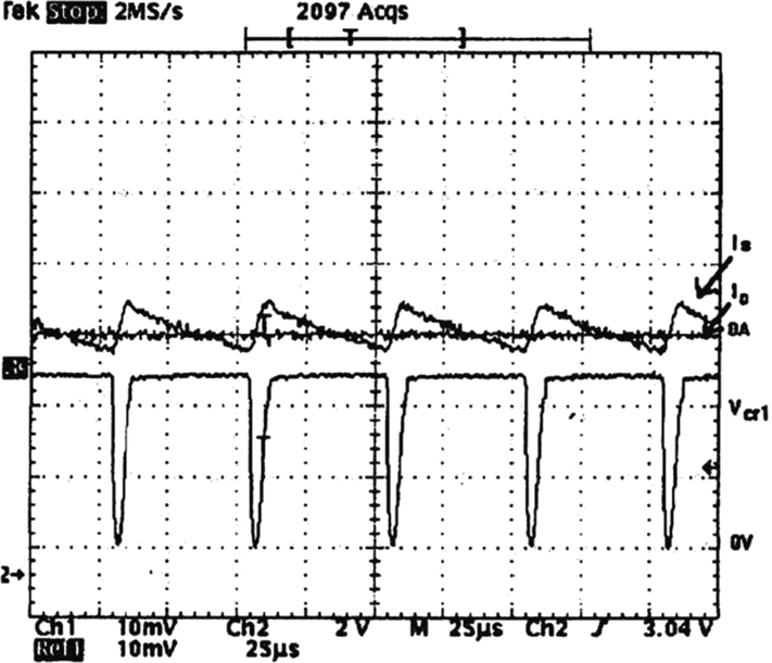
As t3 cannot be determined accurately, a voltage sensor in principle can be used to provide information for t4 so that Sb can be turned on to reconnect C1 to the inverter. In practice, however, Sb can be turned on a few microseconds (longer than Ts+π/ω) after t2 without using a voltage sensor (because it is not critical for Sb to be on exactly at the moment Vcr reaches the nominal voltage). As for switch Sr2, it can be turned on a few microseconds after t4. It will be turned off half of resonant cycle ![]() in the Lr−Cr2 circuit later. In practice, the timing of Sr1, Sr2, and Sb can be adjusted in a simple tuning procedure for a given set of parameters. Fig. 12.58 shows the measured gating signals of Sr1, Sr2, and Sb with the DC link voltage Vcr1 in a 20-kHz switching inverter. Figs. 12.59 and 12.60 show the measured waveforms of Is, Io, and Vcr1 under no-load condition and loaded condition, respectively.
in the Lr−Cr2 circuit later. In practice, the timing of Sr1, Sr2, and Sb can be adjusted in a simple tuning procedure for a given set of parameters. Fig. 12.58 shows the measured gating signals of Sr1, Sr2, and Sb with the DC link voltage Vcr1 in a 20-kHz switching inverter. Figs. 12.59 and 12.60 show the measured waveforms of Is, Io, and Vcr1 under no-load condition and loaded condition, respectively.


12.14.4.3 Control of Quasi-Resonant Soft-Switched Inverter Using Digital Time Control [51]
Based on the zero-average-current error (ZACE) control concept, a digital time control (DTC) method has been developed for a current-controlled quasi-resonant soft-switched inverter. The basic ZACE concept is shown in Fig. 12.61. The current error is obtained from the difference of a reference current and the sensed current. The idea is to make the areas of each transition (A1 and A2) equal. If the switching frequency is significantly greater than the fundamental frequency of the reference signal, the rising and falling current segments can be assumed to be linear. The following simplified equation can be established:

The control algorithm for the inverter is

where ![]() .
.
The schematic of a digital signal processor (DSP)-based controller for the DTC method is shown in Fig. 12.62. The duty cycle can be approximated from the reference sine wave by level shifting and scaling it between 0 and 1. The time tn+2−tn is the sum of Δtn+1 and Δtn+2. These data provide information for the calculation of the next switching time Δtn+1.

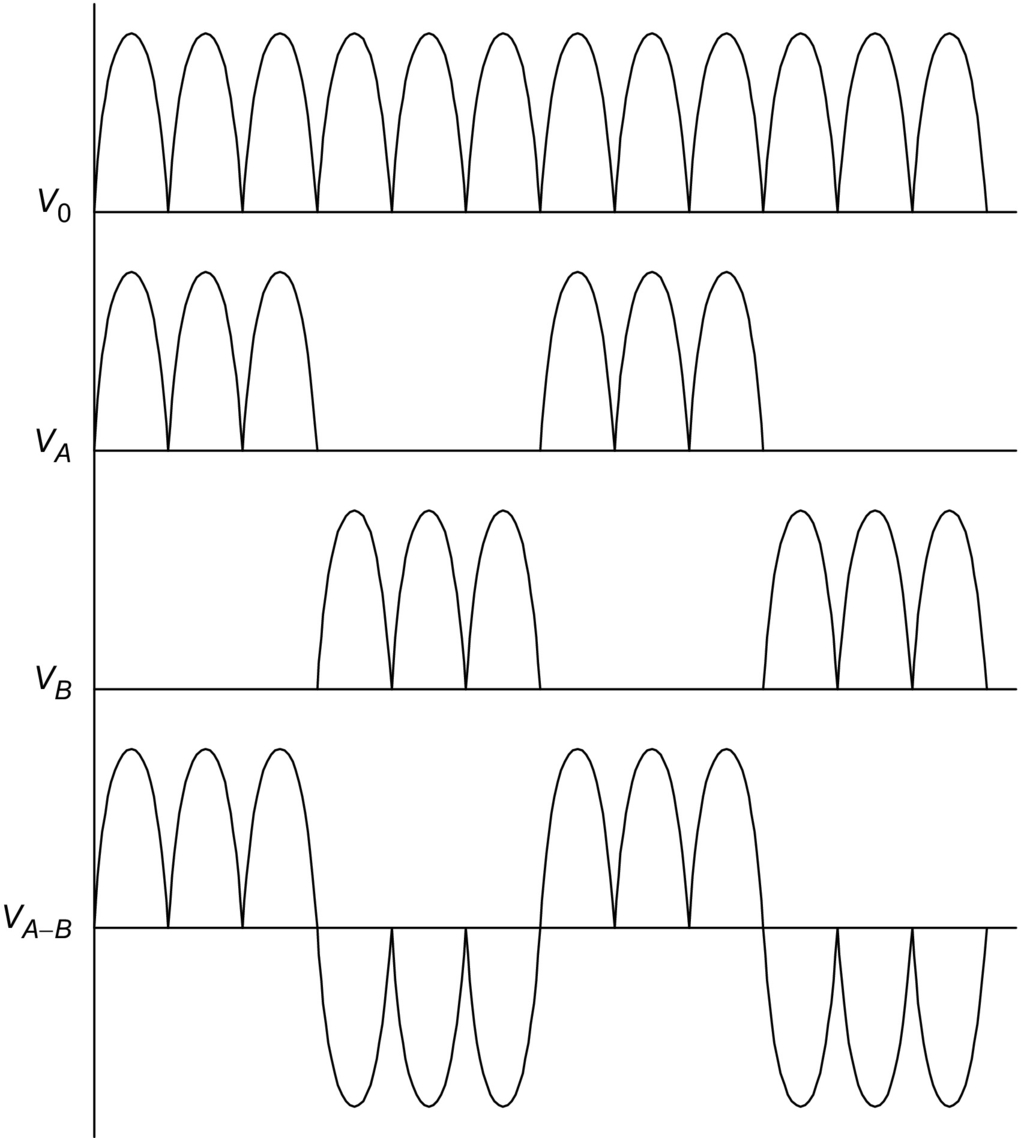
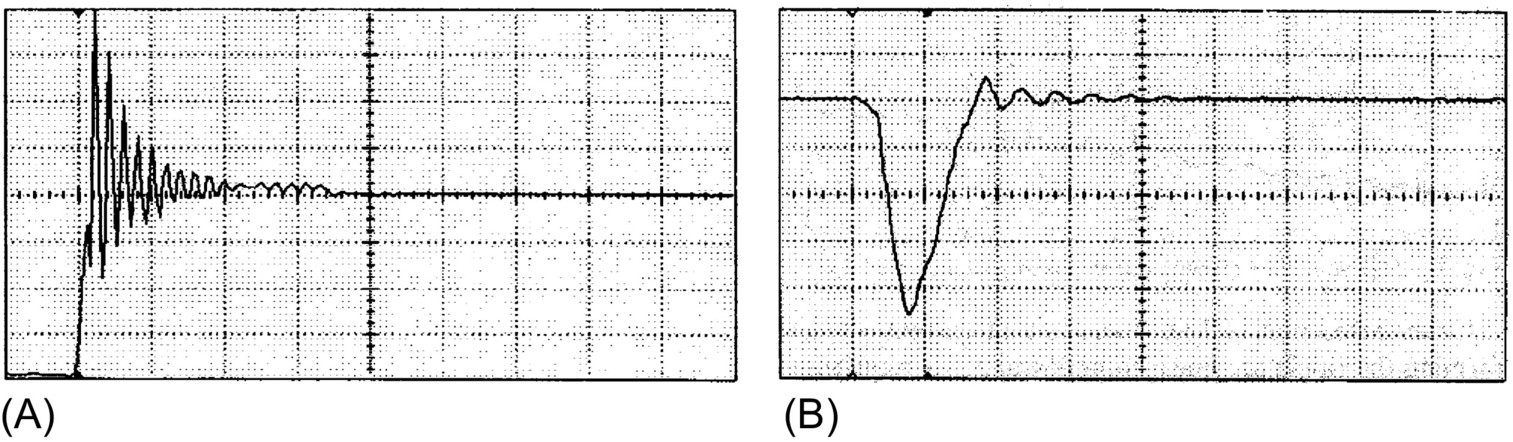
The switches are triggered by the changing edge of the switch control Q. Approximate delays are added to the individual switching signals for both the inverter switches and the quasi-resonant switches. Typical gating waveforms are shown in Fig. 12.63. The use of the quasi-resonant soft-switched inverter is a very effective way in suppressing switching transient and EMI emission. Fig. 12.64A and B shows the inverter switch voltage waveforms of a standard hard-switched inverter and a quasi-resonant soft-switched inverter, respectively. It is clear that the soft-switched waveform has much less transient than the hard-switched waveform.

12.14.5 RPI and ARCPI
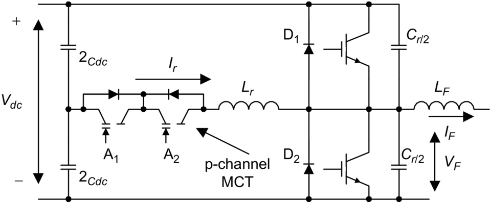
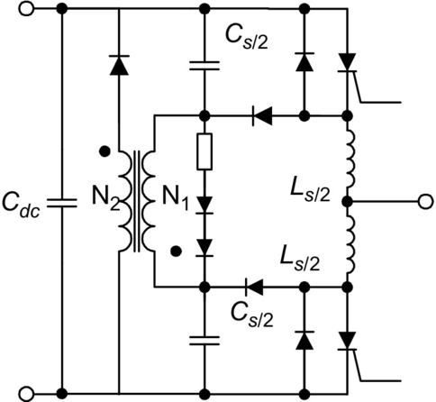
The RPI integrates the resonant components with the output filter components Lf and Cf. The load is connected to the midpoint of the DC bus capacitors as shown in Fig. 12.65. It should however be noted that the RPI can be described as a resonant inverter. Fig. 12.66 shows a single-phase RPI. Its operation can be described with the timing diagram in Fig. 12.67. The operating modes are included in Fig. 12.68. The RPI provides soft switching for all power switches. But it has two disadvantages. First, the power devices have to be switched continuously at the resonant frequency determined by the resonant components. Second, the power devices in the RPI circuit require a 2.2–2.5 p.u. current turn-off capability.


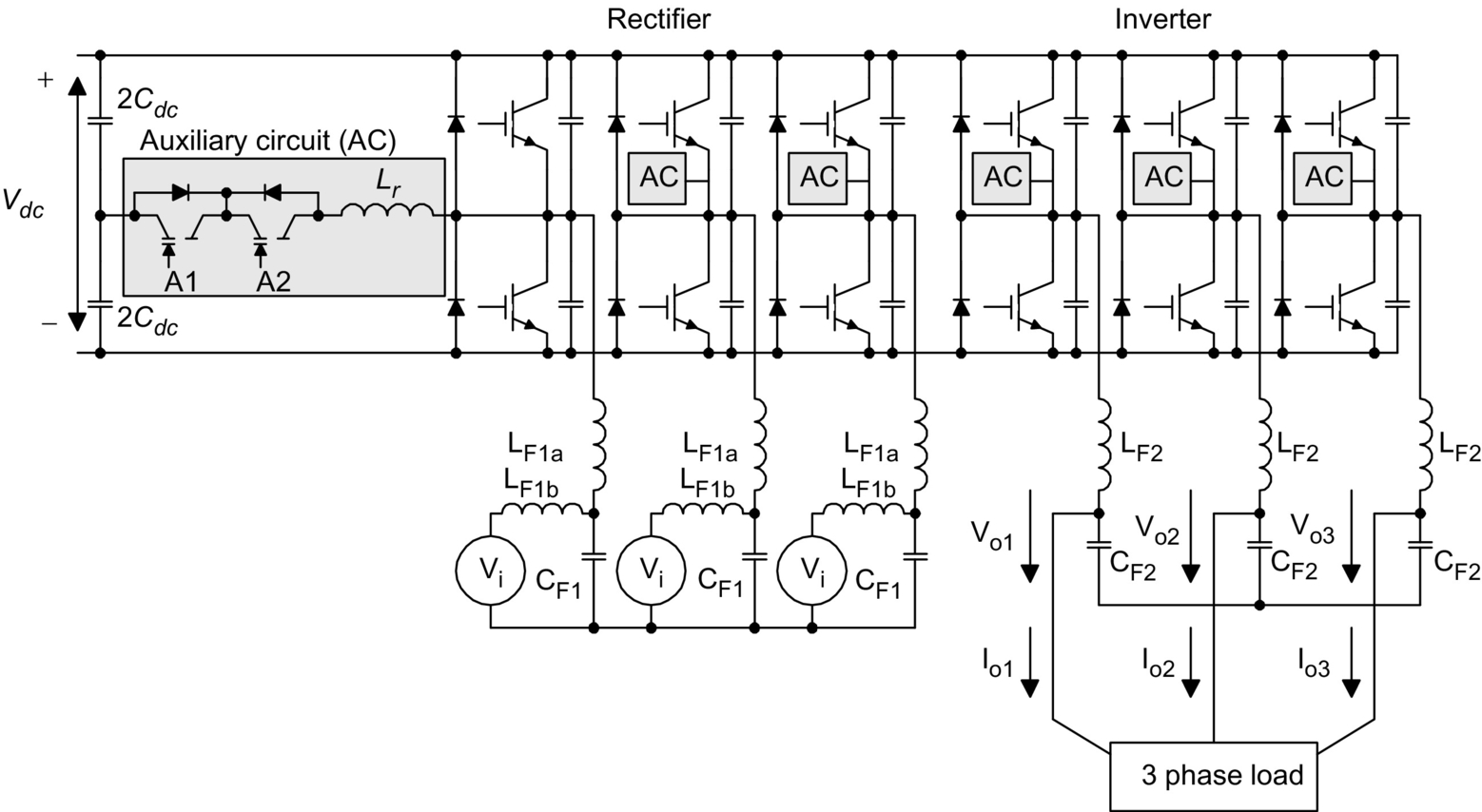
An improved version of the RPI is the ARCPI. The ARCPI for one inverter leg is shown in Fig. 12.69. Unlike the basic RPI, the ARCPI allows the switching frequency to be controlled. Each of the primary switches is closely paralleled with a snubber capacitor to ensure ZV turnoff. Auxiliary switches are connected in series with an inductor, ensuring that they operate under ZC conditions. For each leg, an auxiliary circuit comprising two extra switches A1 and A2, two freewheeling diodes, and a resonant inductor Lr is required. This doubles the number of power switches when compared with hard-switched inverters. Fig. 12.70 shows the three-phase ARCPI system. Depending on the load conditions, three commutation modes are generally needed. The commutation methods at low and high current are different. This makes the control of the ARCPI very complex. The increase in control and circuit complexity represents a considerable cost penalty [52,53].